
 Open Access Article
 This Open Access Article is licensed under a Creative Commons Attribution-Non Commercial 3.0 Unported Licence
Facile synthesis of vacancy-induced 2H-MoS2 nanosheets and defect investigation for supercapacitor application†
Hai Wang *ab,
Xingping Xua and
Anne Nevilleb
*ab,
Xingping Xua and
Anne Nevilleb
aCollege of Mechanical and Electronic Engineering, China University of Petroleum (East China), Qingdao, 266580, China
bInstitute of Functional Surfaces, School of Mechanical Engineering, University of Leeds, Leeds, LS2 9JT, UK. E-mail: mnhw@leeds.ac.uk
First published on 2nd August 2021
Abstract
In this paper, a 2D molybdenum disulfide (MoS2) nanosheet is prepared via a one-step hydrothermal method as electrode material for supercapacitors. Meanwhile, a series of MoS2−x nanostructures with sulfur vacancies have been successfully obtained in an Ar/H2 mixed atmosphere at different annealing temperatures. The prepared materials were characterized by XRD, HR-TEM, Raman and XPS to identify their morphology and crystal properties. MoS2−x assembled by interconnected nanosheets (MoS2−x-700) provides a maximum specific capacitance of 143.12 F g−1 at a current density of 1.0 A g−1 with 87.1% of initial capacitance reserved after 5000 cycles. The outstanding performance of the annealed MoS2−x nanosheets in sodium storage is mainly attributed to the synergistic effect of the unique interconnected structure and the abundant active vacancy generated by the sulfur vacancies. Atomic models of sulfur vacancy defects on the basal plane, Mo-edge and S-edge were established and the electronic properties of MoS2−x were further evaluated assisted by first principles theory. DFT calculation results show that sulfur vacancy defects can provide additional empty states near the Fermi level and induce unpaired electrons, thus increasing the carrier density and improving electrical conductivity. Our findings in this work provide experimental and theoretical evidence of improving the electrochemical performance of 2H-MoS2 nanosheets by annealing treatment.
1. Introduction
In order to resolve the challenge of environmental pollution caused by fossil energy consumption and depletion of non-renewable energy, the utilization of renewable energy such as solar energy, wind energy, hydropower, tidal energy and geothermal energy can effectively reduce the harm of industrial development to nature.1 Developing energy storage and conversion devices with high efficiency and power density is urgent for the purpose of ensuring a sustainable and stable supply of clean energy to supply the production demand.2–5 Electrochemical capacitors (or supercapacitors, SCs) with high power density and long cycle life have become one of the research hotspots due to their excellent power density, fast charge/discharge rate and long-term cycling stability.6–8 Consequently, an ideal electrode material for SCs should meet the requirement of high specific surface area, high exposure active sites, excellent conductivity, suitable pore size distribution and good electrolyte wettability.9–11Two-dimensional nanomaterials with special properties have immeasurable application potential in the fields of semiconductors, microelectronics and biomedicine, and have attracted global attention from scientists around the world.12–16 In particular, molybdenum disulfide (MoS2) is considered to be one of the most promising two-dimensional materials due to its low cost, environmental friendliness, natural abundance and ease of manufacturing.17–19 The layered structure of MoS2 is similar to graphite in which the hexagonal layer of Mo is sandwiched between two S layers. Mo–S is bonded by strong covalent bonds while S–S is interacted by weak van der Waals forces. In particular, the highly stable 2H-MoS2 has unique properties based on its thickness. Its ultrathin planar structure provides an ideal platform for flexible adjustment of electronic structure and surface characteristics through surface and/or interface functionalization.20 Hao21 used a simple hydrothermal method to reasonably modulate and coaxially arrange the in-plane 1T–2H MoS2 heterostructure (MoS2/CF) on three-dimensional carbon nanofibers. The MoS2/CF composite shows a high specific capacitance of 310 F g−1 and a remarkable rate performance of 78% at 100 mV s−1. Manufactured asymmetric supercapacitor provides an impressive energy density of 81.4 W h kg−1 in 1 M Na2SO4 electrolyte. Shanu22 reported a three-dimensional MoS2 nanoflower with a hexagonal (2H) phase for supercapacitor applications with a high specific capacitance of 382 F g−1 at a current density of 1 A g−1. The symmetrical solid supercapacitor device with 2H-MoS2 nanoflower electrode and PVA-Na2SO4 electrolyte exhibits an energy density of 16.4 W h kg−1 and a retention rate of 97.5% after 4000 cycles. However, pristine MoS2 displays poor electrochemical behavior during the charge/discharge processes due to structural agglomeration and slow reaction kinetics.
As a common type of surface defect, vacancy has been considered to play an important role in many catalytic reactions of transition metal compound catalysts.23,24 Vacancy/defect engineering is indeed a potentially effective strategy to improve the electrochemical performance of electrodes in different energy storage devices. The generation of vacancies/defects leads to a wider layer spacing, which accelerates ion insertion and extraction and ensures the stability of the electrode structure during continuous charging/discharge.25,26 Density functional theory (DFT) is one of the most commonly used methods in the field of computational chemistry to investigate electronic structures.27–29 The combination of DFT calculations and micro-dynamic models can be used to establish a direct relationship between electrochemical properties and vacancy types, not only to determine the optimal vacancy structure, but also to understand the mechanism of the key factors to improve the conductivity of the material.
Herein, we report the facile synthesis of nanostructured MoS2 and a series of MoS2−x composites with sulfur vacancy defects assisted by one-step hydrothermal process and annealing treatment at different temperatures as electrode materials for sodium ion supercapacitors. The samples were characterized by TEM, XRD, XPS, and Raman spectroscopy to study the effect of vacancy defects on the structure and electrical properties of MoS2. After annealing at 700 °C, the specific capacitance of the MoS2 nanosheets increases from 97.5 F g−1 to 142.3 F g−1, and 87.1% of the initial capacitance is reserved after 5000 charge/discharge cycles (1.0 A g−1). The gaps formed by the interlaced nanosheets furnish the electrode surface with fast and efficient channels for electrolyte penetration and easy charge transfer (intercalation/deintercalation), while larger interplanar distance achieved by annealing process provides more active sites for reversible redox reactions, thus increasing the electrical conductivity and specific capacitance. Hence, first-principles density functional theory (DFT) calculation was carried out to understand the improving electrochemical performance of MoS2−x benefited from S vacancies at atomic level. Computational result is in good agreement with the experiment data and this strategy provides fundamental insights into utilizing two-dimensional materials towards energy storage applications.
2. Materials and methods
2.1 Material preparation
Sodium molybdate (Na2MoO4·2H2O) and thiourea (CH4N2S) were purchased from Sigma-Aldrich. Hydrochloric acid (HCl) was purchased from VWR Chemicals (USA). Sodium sulfite (Na2SO3), polyvinylidene fluoride (PVDF) and acetylene black were bought from Alfa Aesar. The deionized water was supplied by a Water Purifier system. All the chemicals were used as received without further purification.2.2 Synthesis of MoS2 nanosheet and MoS2−x
MoS2 nanosheets are synthesized in one step by hydrothermal method. In a typical experiment, 0.618 g Na2MoO4 and 0.837 g thiourea were dissolved in 50 ml of deionized water and mixed for 30 minutes under magnetic stirring. The pH of the solution was adjusted to 1 by adding 12 M hydrochloric acid. The solution was then transferred to a 100 ml autoclave lined with Teflon and heated at 180 °C for 24 hours. The obtained product was then precipitated and washed with deionized water and ethanol, centrifuged at 10![[thin space (1/6-em)]](https://www.rsc.org/images/entities/char_2009.gif) 000 rpm for 5 minutes several times, and finally dried in an oven at 70 °C for 12 hours. In order to obtain sulfur vacancy defect, the sample was then annealed at 300 °C, 500 °C and 700 °C in Ar (95%) + H2 (5%) for 3 h until MoS2 was reduced to MoS2−x. The samples were labeled as MoS2−x-300, MoS2−x-500 and MoS2−x-700 respectively according to the calcination temperature.
000 rpm for 5 minutes several times, and finally dried in an oven at 70 °C for 12 hours. In order to obtain sulfur vacancy defect, the sample was then annealed at 300 °C, 500 °C and 700 °C in Ar (95%) + H2 (5%) for 3 h until MoS2 was reduced to MoS2−x. The samples were labeled as MoS2−x-300, MoS2−x-500 and MoS2−x-700 respectively according to the calcination temperature.
2.3 Material characterization
The morphology of the products was observed by Transmission Electron Microscope (TEM, JEM 2100), the crystal structure of the composites was obtained using X-ray photoelectron spectroscopy (XPS, Thermal Scientific ESCALAB Xi+), X-ray diffraction (Rigaku XRD ULTIMA IV), Raman spectroscopy was performed using Renishaw invia qontor (532 nm).2.4 Fabrication of MoS2 and MoS2−x electrodes
The prepared MoS2 and MoS2−x, acetylene black and PVDF were mixed at a weight ratio of 8:1:1 and mixed to a uniform slurry and spread on an aluminum foil. Afterwards the foil was dried for 12 h at 100 °C in a vacuum oven. After drying, 10 MPa pressure was applied to the electrode, thereby improving the stability and electrochemical performance of the electrode. Afterward, the electrode was cut into a square chip (area = 1 cm × 1 cm). Specifically, the loading amounts of MoS2 were calculated and listed in Table S1† by comparing the weight difference of aluminum foil before and after coating.
2.5 Electrochemical characterization
Electrochemistry tests were conducted in a standard three-electrode system. The electrolyte is 1 mol L−1 Na2SO3 solution with the platinum foil as the counter electrode and a saturated silver/silver chloride as the reference electrode. The galvanostatic charge/discharge tests (GCD) at various current densities were performed using a LAND CT-2001A battery test system (Wuhan Jinnuo Electronics Co., Ltd) cyclic voltammetry (CV) and electrochemical impedance spectroscopy (EIS) tests were performed at room temperature using an ACM Gill 1800 electrochemical workstation. CV measurement was performed at a potential range of −1.0 V and −0.2 V versus silver/silver chloride. The AC impedance test frequency ranged from 100 kHz to 10 mHz. The specific capacitance is calculated from GCD according to eqn (1).30
 | (1) |
3. Results and discussion
3.1 Crystal structure and morphology characterizations
The formation process of MoS2 nanosheet and MoS2−x samples annealed at different temperature is illustrated in Fig. 1. Precursor solution containing MoO4− is hydrothermally processed in a Teflon-based autoclave at 180 °C to obtain pristine MoS2 nanosheet. Afterwards the MoS2 was placed in a furnace where the temperature was set as 300 °C, 500 °C and 700 °C for annealing treatment. Reactions happened in the autoclave during hydrothermal process are shown in eqn (2) and (3).| NH2CSNH2 + H2O → NH3 + H2S + CO2 | (2) |
| Na2MoO4 + H2S → MoS2 + Na2SO4 + H2O | (3) |
 | ||
| Fig. 1 Schematic diagram of fabrication process of MoS2 nanosheet and MoS2−x electrodes. | ||
The crystal structure, morphology and microstructure of MoS2−x composites were studied by XRD, SEM, XPS and UV spectra. X-Ray diffraction pattern in Fig. 2(a) of the solvent-assisted pristine MoS2 nanosheets shows the characteristic peaks located at 14.3°, 33.5°, 39.6°, 44.2°, 49.8°, 58.5° and 60.2° can be well indexed to (0 0 2), (1 0 1), (1 0 3), (0 0 6), (1 0 5), (1 1 0) and (0 0 8) crystal plane of 2H phase MoS2 (JCPDS no. 37-1492). The crystal phase of MoS2−x annealed at 300 °C, 500 °C and 700 °C were also obtained by XRD analysis. The samples after annealing exhibit slight intensity difference, which can be attributed to vacancies and defects caused by annealing.31 The negative shift of (0 0 2) peak may be related to the T-MoS2 phase produced during annealing. Characteristic peak of MoS2 without annealing is wide, indicating that the crystallinity is low before annealing. As annealing temperature increases from 300 °C to 700 °C, the diffraction peak becomes relatively stronger and sharper, indicating a better crystallization process at high annealing temperature. Such change of peak intensity with post annealing process may be related to the removal of lattice disorder and the smear of signal from S vacancy in MoS2 nanosheets.32
 | ||
| Fig. 2 (a) XRD patterns and (b) Raman analysis of MoS2 and MoS2−x. | ||
The Raman spectra of MoS2 and MoS2−x are shown in Fig. 2(b). All samples show two main peaks near 375.84 cm−1 and 402.5 cm−1 corresponding to the in-plane E12g and out-of-plane A1g vibration modes of MoS2, respectively. The slight shift and enhanced width of characteristic peaks 375.84 cm−1 with the increase of annealing temperatures may be attributed to the loss of sulfur in MoS2−x samples, which agrees well with previous reports.33,34
Fig. 3(a)–(c) show the low resolution TEM image of synthesized 2H-MoS2, which has a typical two-dimensional exfoliated structure and the nanosheet structure shows good dispersion. Fig. 3(d)–(f) display the low-resolution TEM images of the MoS2−x nanosheet. After annealing treatment, MoS2−x exhibits very similar morphology and structure, indicating that annealing atmosphere and temperature has no special effect on crystal morphologies. It is also clear that the average thickness of 2H-MoS2−x nanosheets is about 10 nm and the lateral size falls into a scale range from approximately 50 nm to 100 nm. In addition, these prepared nanosheets are interlinked with each other, which endows them with abundant open gaps and electrochemically active sites, thus forming the typical characteristics of mesoporous structure. Fig. 3(g)–(i) demonstrate the high-resolution TEM images (HRTEM) of interlayer distance corresponding to the (0 0 2) crystal plane of MoS2−x annealed at 300 °C, 500 °C and 700 °C, respectively. In contrast, 2H-MoS2 samples annealed at 700 °C have the maximum layer spacing of 0.628 nm and matches perfectly with crystalline MoS2 of 0.63 nm.35 The increased layer spacing is conducive to the rapid diffusion and embedding of electrolyte ions in the process of rapid charge/discharge, which is beneficial in achieving excellent rate performance for supercapacitors.36,37
 | ||
| Fig. 3 (a)–(c) TEM image of 2H-MoS2 at low resolution; (d)–(f) TEM image of MoS2−x at low resolution and HRTEM of (g) MoS2−x-300 (h) MoS2−x-500 (i) MoS2−x-700 and corresponding interlayer distance. | ||
The valence states and chemical compositions of the original MoS2 and MoS2−x-700 were further studied by XPS to evaluate the effect of annealing process on surface charge states. Fig. 4(a) shows the high-resolution spectra of Mo-3d in pristine MoS2. A pair of characteristic peaks at 232.47 and 229.35 eV can be indexed to Mo 3d3/2 and Mo 3d5/2 doublet originated from Mo4+. Apart from a pair of characteristic peaks from Mo4+ at 232.47 and 229.35 eV, small subpeaks belonging to the Mo6+ 3d5/2 and Mo6+ 3d3/2 were also observed at 233.10 and 236.45 eV, indicating that the presence of Mo6+ is associated with the surface oxidation of MoO3, which could be readily detected in XPS spectra.38–40 There is a peak near 226.53 eV, which corresponds to the S–S bond formed by residual sulfur that has not reacted with molybdenum. According to Fig. 4(b), in the high-resolution spectra of S-2p, the double peaks at 163.30 eV and 162.11 eV are derived from S 2p1/2 and S 2p3/2 of S2−, providing conclusive evidence for the existence of MoS2. The S 2p XPS spectra of all MoS2 exhibit two satellite peaks at 168.84 eV (S 2p3/2) and 170.05 eV (S 2p1/2) which is consistent with S6+ species in sulfate groups. Compared with pristine MoS2, characteristic peak of Mo 3d3/2 in MoS2−x-700 in Fig. 4(c) moved from the initial position of 232.47 eV to 232.19 eV, while the peak of Mo 3d5/2 shifted from 229.35 eV to 229.04 eV in MoS2−x-700 after annealing process (BE shift of Mo 3d5/2 = 0.31 eV and Mo 3d3/2 = 0.28 eV), indicating slight electron transfer to Mo for enhancing the H adsorption during the chemical reduction.41,42 The Mo 3d peak position of the S vacancy sample deviates slightly from the original sample, which also confirms the existence of defects. After annealing in 95% Ar + 5% H2 mixed atmosphere, peak intensity of Mo6+ 3d5/2 (232.94 eV) and Mo6+ 3d3/2 (235.99 eV) related to MoO3 and S 2s peak of unreacted residual sulfur become weaker, indicating both the content of impurity oxygen and unreacted sulfur in MoS2−x layer obviously decrease.43 In Fig. 4(d), it is worth noting that the S 2p peak of MoS2−x-700 shifted to a relatively higher binding energy (BE shift of S 2p3/2 = 0.37 eV and S 2p1/2 = 0.39 eV), indicating that more S vacancies were introduced in these products.44 Quantitative analysis of atomic ratio in Fig. S3† also confirms that more S vacancies were found at higher annealing temperatures, which accelerates the transfer of electrons from sulfide to sulfur vacancies, thereby reducing the equilibrium electron cloud density and enhancing the binding energy.45 S 2s core-level spectra is not sensitive to annealing temperature, and there is no major peak shift. All these demonstrates that S vacancies do exist in MoS2−x after annealing in Ar + H2 mixed atmosphere.
 | ||
| Fig. 4 High-resolution XPS spectra of (a) Mo 3d of MoS2, (b) S 2p of MoS2, (c) Mo 3d of MoS2−x-700, (d) S 2p of MoS2−x-700. | ||
3.2 Electrochemical measurement
The electrochemical properties of MoS2−x composites were evaluated in a three-electrode cell in a 1.0 M Na2SO3 solution. In Fig. 5(a), the cyclic voltammetry (CV) of MoS2−x-700 at different scanning rates from 2.5 to 50 mV s−1 showed a stable potential window from −1.0 V to −0.2 V. The peak current increases gradually with the increase of the scanning rate, indicating the fast diffusion control kinetics of ion transport at interface between electrode and electrolyte. The CV curve at different scanning rate shows a quasi-rectangular shape without significant redox peaks, indicating that both pseudocapacitive and electrical double-layer capacitive behaviors are simultaneously occurring in the electrostatic process.46–49 The CV curve maintains a quasi-rectangular shape at high scan rates, indicating the pseudocapacitor effect and high rate performance of MoS2−x. Comparable CV result of MoS2, MoS2−x-300, MoS2−x-500 is illustrated in Fig. S1.†The charge storage mechanism on the MoS2 electrode can be explained by two processes, namely (i) surface capacitance involving ion adsorption/desorption process, and (ii) embedding capacitance involving electrolyte ion insertion/de-intercalation into the MoS2 nanosheet, which can be explained by eqn (4) and (5).50,51| (MoS2)surface + Na+ + e− ⇄ (MoS−2–Na+)surface | (4) |
| MoS2 + xNa+ + xe− ⇄ NaxMoS2 | (5) |
 | ||
| Fig. 5 (a) CV curves of MoS2−x-700 electrode at various scan rates (b) GCD curves of MoS2−x-700 electrode at various current densities (c) CV curves of MoS2−x-700 electrode at initial 4 cycles (d) specific capacitances of MoS2, MoS2−x-300, MoS2−x-500 and MoS2−x-700 calculated from GCD. | ||
In order to understand the potential change with time during charge and discharge process, the GCD curve of the MoS2−x-700 electrode at current densities of 0.5 A g−1, 1.0 A g−1, 2.0 A g−1, 3.0 A g−1 and 5.0 A g−1 is achieved and illustrated in Fig. 5(b). The GCD curve of MoS2−x-700 shows an approximately symmetrical triangular shape with reasonably linear slopes, which demonstrates that the charge and discharge process of MoS2−x-700 is an ideal capacitance behavior and further confirms the high rate characteristics and ideal capacitive performance of the electrode.52–54 At different current densities, the non-symmetrical part of the charge–discharge curve indicates that the supercapacitive behavior of the MoS2 supercapacitor is dominated by the Faraday charge transfer process. The charge/discharge time at higher current density is shorter because the electrode material cannot be charged immediately, which makes it difficult for the redox reaction to keep up with the rapid change in voltage. Further, GCD curve of MoS2−x can be approximated as linear slope with small voltage drop, indicating that MoS2−x electrode has excellent redox reversibility and good electrochemical stability.
To understand the material degradation happened on the electrode surface, the CV change of the MoS2−x-700 electrode in the initial 4 cycles at a scan rate of 2.5 mV s−1 is described in Fig. 5(c). The most obvious difference is that the oxidation peak appeared at about −0.25 V and −0.67 V in the first cycle and then disappeared immediately after the end of the cycle. In the first cycle, the irreversible capacity drop may be due to the formation of the solid electrolyte interfacial phase (SEI) membrane and the irreversible Na+ insertion. But after the first two cycles, the discharge and charge capacity tended to be stable, and the subsequent cycle discharge and charge voltage graphs almost overlap. It is further confirmed that the MoS2−x-700 electrode possess highly reversible sodium storage behavior. The oxidation–reduction reaction that occurred in the first week of the voltammetry cycle test can be revealed by eqn (6) and (7).55,56
| 2Na+ + nS + 2e− → Na2Sn (4 ≤ n ≤ 8) | (6) |
| NaxMoS2 + (4 − x)Na+ + (4 − x)e− → 2NaxS + Mo | (7) |
According to the CV scan at first cycle, the reduction peak near −0.25 V is derived from the small amount of sulfur in MoS2−x that has not reacted with Mo on the electrode surface (confirmed by the S–S bond in XPS spectra) was transformed into the long-chain polysulfide compounds (Na2Sn, 4 ≤ n ≤ 8), and further reduced to short-chain polysulfide compounds (Na2S and Na2S2).57 The oxidation peak at −0.39 V is due to the sectional oxidation of Mo metal to form MoS2. Another reduction peak located near −0.67 V can be explained by the further conversion of NaxMoS2 into the NaxS matrix and metallic Mo, which is described as the irreversible reduction reaction in eqn (4).
The specific capacitance shown in Fig. 5(d) is calculated from GCD curves according to eqn (1). It can be seen that the MoS2−x-700 composite material has the highest capacitance. Cs value of 170.2 F g−1, 142.2 F g−1, 121.1 F g−1, 109.3 F g−1 and 91.8 F g−1 is achieved at current density of 0.5 A g−1, 1.0 A g−1, 2.0 A g−1, 3.0 A g−1, and 5.0 A g−1, respectively. Specific capacitance of the electrode decreases in the order of MoS2−x-700, MoS2−x-500, MoS2−x-300 and MoS2 at each charge/discharge current density, which is in consistent with the order of the area enclosed by the CV curve in Fig. S1.†
The ion transport kinetics of MoS2 and MoS2−x electrodes during electrochemical reaction were measured by electrochemical impedance spectroscopy (EIS). Equivalent circuit fitting of MoS2 and MoS2−x is composed of pure capacitance element (C), equivalent series resistance (ESR), charge transfer resistance (Rct) and Warburg resistance (W). Nyquist diagram in Fig. 6(a) can be divided into three parts. The intercept on authentic composition Z′ of the high-frequency Nyquist diagram indicates that the equivalent series resistance (ESR) which consists of the resistance of the electroactive material, the resistance of the solution, and the contact resistance at the interface.58,59 The corresponding ESR values are 1.89 Ω, 1.42 Ω, 1.21 Ω and 0.87 Ω for MoS2, MoS2−x-300, MoS2−x-500 and MoS2−x-700 respectively. The charge transfer resistance (Rct) generated by the Faraday redox process can be obtained from the diameter of the semi-circle in the intermediate frequency region, of which the values are 7.25 Ω, 4.31 Ω, 3.99 Ω and 3.75 Ω for electrodes based on MoS2, MoS2−x-300, MoS2−x-500 and MoS2−x-700. Low Rct value indicates an improved conductivity and charge transfer speed of MoS2−x after annealing. The straight line at low frequency regime represents the Warburg region, which is related to diffusion of electrolyte ions to the reaction interface. The approximately parallel line to the virtual Z′′ axis from the low frequency region can reflect the ideal capacitance behavior of the material. MoS2−x nanosheets annealed at 700 °C significantly reduces the diffusion path length of electrolyte ions and electrons, thus increasing the diffusion and migration rate of electrolyte ions in the process of charge and discharge.60 In addition, voids scattered between the nanosheets can promote the transfer rate of electrolyte ions and avoid volume changes during charge/discharge.61
 | ||
| Fig. 6 (a) Nyquist plots of MoS2, MoS2−x-300, MoS2−x-500 and MoS2−x (b) cycling performance of MoS2, MoS2−x-300, MoS2−x-500 and MoS2−x-700 within 5000 cycles. | ||
The stability of the energy storage device is a crucial parameter in supercapacitor application. The stability of the MoS2 and MoS2−x electrodes were evaluated for 5000 cycles between −1.0 and −0.2 V at a current density of 1.0 A g−1, and the capacitance retention of the MoS2 asymmetric supercapacitor is shown in Fig. 6(b). After 5000 cycles, the supercapacitors based on MoS2 and MoS2−x annealed at 300 °C, 500 °C and 700 °C retained 75.2%, 70.8%, 81.8% and 87.1% respectively of their initial capacitance. The slight decrease in capacitance can be ascribed to the accumulation of structural defects and the repeated expansion and contraction of the electrode material during charge and discharge.62,63 It shows that most of the charge accumulated during the charging process can be fully released during the discharge and further confirms that the MoS2−x nanosheet after annealing treatment is stable and robust as a promising candidate for sodium-ion supercapacitor.
The electrochemical performance of MoS2−x after annealing process material is significantly improved due to the synergistic effect of S vacancies and unique nanosheet structure. The interconnected nanosheets provide abundant diffusion channels, allowing the electrolyte to fully penetrate and reducing the diffusion paths for electrons and Na+ ions, thereby obtaining a larger specific capacitance. On the other hand, increased number of vacancy defects at higher annealing temperature not only improve the conductivity of the active material, but also greatly increase the number of active sites and provide an expanded interlayer spacing, which makes the charge transfer faster and endows more reversible redox reactions in the process of charge and discharge. Annealing treatment up to 700 °C helps MoS2 nanosheets to release the strain caused by the continuous insertion and extraction of Na+, thereby inhibiting the volume expansion of the electrode material and resulting in better cyclic stability.
3.3 DFT calculation
In order to support the experimental results qualitatively and provide theoretical evidence for charge transfer possibility between different orbitals of the structures with S vacancy, DFT was used to study the effect of vacancy on MoS2 at atomic level. Calculation was implemented using a Vienna Ab Initio Simulation Package (VASP) code with Projection Enhanced Wave (PAW) pseudopotential used to perform density functional theory (DFT).64,65 Generalized gradient approximation (GGA) function is employed to calculate exchange–correlation energy. The cut-off energy of the extended plane-wave base is set to 500 eV. Throughout the work, spin polarization calculations were carried out. The position of the atoms is relaxed until the force acting on each atom becomes less than 0.01 eV Å−1.In this work, we use the 2H phase of monolayer of MoS2 in computational simulation which is stable at room temperature. The primitive cell consists of 4 Mo atoms in the x direction and 4 S atoms in the y direction. In order to save calculation time, the bottom two layers of atoms are held in place, and the top two layers are relaxed in the calculation. For the Brillouin zone samples, we use 5 × 5 × 1 k-point grids for 3 × 3 × 1 supercell. The supercell includes a vacuum with a thickness of at least 15 Å to minimize the interaction between repeated images in the vertical direction within periodic boundary conditions.
To evaluate the effect of S vacancy on the electrochemical properties of MoS2−x composites, three different types of MoS2 with S vacancy have been studied as calculation models. Schematic diagram of pristine MoS2 model, MoS2−x models with S vacancy in the basal plane (B-V), S vacancy located at the edge of Mo atom (Mo-V) and S vacancy located at the edge of S atom (S-V) is shown in the Fig. 7. The partial density of states (PDOS), total density of states (DOS) and differential charge density of three different types of MoS2 structures with S vacancies were calculated to understand the effect of S vacancy on electronic properties compare the electrochemical reactivity of these structures.
 | ||
| Fig. 7 Schematic model of pristine MoS2 and MoS2−x with three kinds of vacancy defects. | ||
PDOS result of the pristine 3 × 3 × 1 single-layer MoS2 is shown in Fig. 8(a). As can be seen from the figure, the valance band maximum (VBM) is composed of strong Mo-4d state and weak S-3p state, while conductive band minimum (CBM) is mainly composed of Mo-4d state. In this state, there is no electron state passing through at Fermi level, while MoS2 near Fermi level is mainly contributed by Mo-4d, indicating the pristine MoS2 without S atom defect presents semiconductor properties at this time. In the range of −6 eV to −2 eV of the valence band, the Mo-4d states overlap with the S-3p states especially at peaks around −3.88 eV and −1.98 eV, indicating an orbital hybridization effect. PDOS result of MoS2−x with B-V defect is illustrated in Fig. 8(b). Similarly, the valence band is mainly contributed by the electronic states of Mo-4d and S-3p, and the conduction band is dominated by Mo-4d states. Local hybridization effect also appears in the orbitals of Mo-4d and S-3p in the range of −6 eV to −2 eV. Compared with the PDOS of pristine MoS2 structure, the main difference is that several new peaks from −0.4 eV to 0 eV in Mo-4d orbit appear near Fermi level, which indicates that the introduction of S vacancy in basal plane provides more available states for MoS2 around Fermi level for electron acceleration and migration.
 | ||
| Fig. 8 PDOS of (a) pristine MoS2 and (b) MoS2−x with B-V defect. | ||
Fig. 9(a) shows the PDOS of structure with S vacancy at the edge of Mo atom (Mo-V). In this state, electron states pass through the Fermi level, indicating the MoS2 with this defect behaves as a conductor. Compared with the B-V defect, there are more energy states in the Mo-4d orbitals near the Fermi level, which can be explained by the fact that Mo atoms on the edge of Mo coordinate with fewer S atoms, resulting in more empty 4d states. The Mo-4d orbital energy states of defect structure are also enhanced compared with structure with B-V defect. PDOS of structure with S vacancy defect at the edge of the S atom (S-V) is illustrated in Fig. 9(b). The main peak of the electronic density distribution in the valance band lies at −12.0 eV with a remarkable increase in density. New empty states were introduced in the Mo-4d orbit and states intensities were enhanced between −0.3 eV and 0.3 eV, which indicates S vacancies increase the carrier density near the Fermi level and helps trap carriers and transit to the ground states through non-radiative recombination.66,67 The DOS results in ESI (Fig. S2†) further illustrate the electronic improvement due to S vacancies. The number of spin-up and spin-down electrons are the same in the pristine MoS2 and MoS2−x with B-V defect, indicating the extranuclear electrons have been paired with structural stability. In contrast, the numbers of spin-up and spin-down electron are different in MoS2−x with Mo-V and S-V defects, indicating that unpaired electrons exist in the structures. S-V defects shows greater asymmetry with more unpaired electrons than Mo-V defect. These electrons can easily migrate in electric field during charge and discharge, thereby increasing the reaction current and specific capacitance. Both DOS and PDOS results indicate that S-V defect provides maximum improvement in conductivity and specific capacitance of MoS2.
 | ||
| Fig. 9 PDOS of (a) MoS2−x with Mo-V defect and (b) MoS2−x with S-V defect. | ||
The differential charge density result after 1 × 2 × 1 cell expansion of different vacancy defect models with an isosurface value of 0.008 e Å−3 is shown in Fig. 10, where yellow area represents the charge accumulation and blue region indicates that the amount of electron is reduced. The differential charge density diagrams with different S vacancy defects show a substantial charge transfer, which is mainly ascribed to the redistribution of charge within the layer.68 Most differential charge density graphs near the S vacancies are shown in blue, which means that electron loss occurs in the S vacancies. To summarize, S vacancies break symmetry and cause dangling bonds on adjacent Mo atoms, which allows interstitial states and improves conductivity. In particular, S-V defect shows greatest contribution in improving the conductivity and specific capacitance of MoS2−x due to the unstable electronic structures.
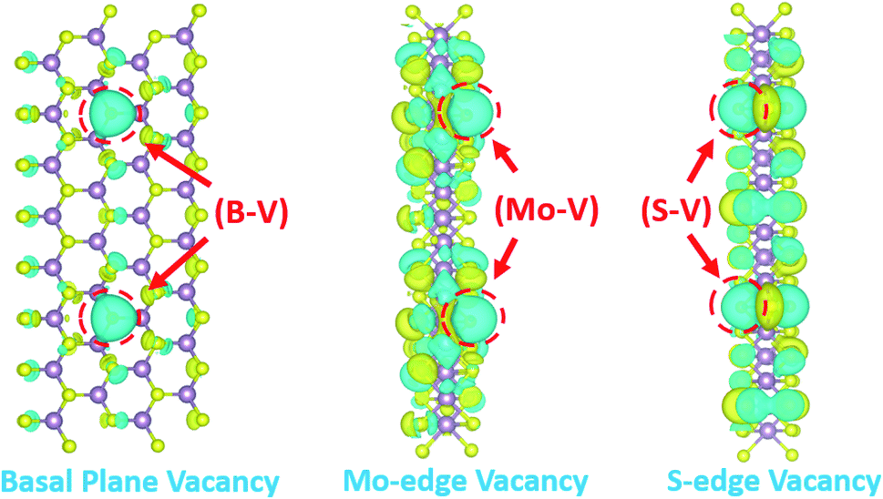 | ||
| Fig. 10 Differential charge density of MoS2−x with B-V, Mo-V and S-V defects. | ||
Excellent electrochemical properties obtained at 700 °C can be attributed to two aspect. Structurally, higher annealing temperatures means better crystallinity and larger spacing, both of which provide abundant diffusion channels for Na+ and electrons. On the other hand, higher temperature means more sulfur vacancies, among which S-V defect shows greatest contribution in improving the conductivity and specific capacitance of MoS2−x due to the unstable electronic structures. It provides more opportunities for Mo atoms to coordinate with fewer S atoms and creating more empty 4d states, which is supported by DFT calculation. These empty states allow electrons easily migrate and increase carrier mobility, thus obtaining the highest capacitance and achieving the best properties at 700 °C.
Table 1 compares several MoS2 related materials used in supercapacitors regarding specific capacitance, electrolyte, current density and capacitance retention. The strategy of synthesizing vacancy-induced MoS2−x by implementing annealing treatment remarkably increases the capacitance and improves the supercapacitor performance of pristine MoS2. Hence, it offers enormous opportunities in fabricating MoS2-based nanosized composites with enhanced capacitance and better performance. Based on our findings, preparations of MoS2 derivatives with complex structures and superior properties will be continued in the future work.
| Electrode | Electrolyte | Current density | Specific capacitance | Retention rate | Reference |
|---|---|---|---|---|---|
| MoS2 nanosheet | 1.0 M Na2SO4 | 1.0 A g−1 | 129.2 F g−1 | 85.0% | 69 |
| MoS2 nanoworm | 1.0 M Na2SO4 | 1.0 A g−1 | 138.0 F g−1 | 86.0% | 70 |
| MoS2@Ti plate | 1.0 M KCl | 1.0 A g−1 | 133.0 F g−1 | 93.0% | 71 |
| MoS2/graphene | 1.0 M Na2SO4 | 1.0 A g−1 | 243.0 F g−1 | 82.5% | 72 |
| 2H-MoS2 | 1.0 M Na2SO3 | 1.0 A g−1 | 142.3 F g−1 | 87.1% | This work |
4. Conclusions
In conclusion, two-dimensional MoS2 nanosheets with 2H phase were synthesized by one-step hydrothermal method and sulfur vacancy defects were strategically introduced into the samples by annealing treatment method. The structure, morphology, elemental composition and valence state of MoS2 and MoS2−x with S vacancies were studied by XRD, HR-TEM, XPS and Raman analysis. Electrochemical measurements show that the MoS2 calcined at temperature of 700 °C in Ar (95%) + H2 (5%) has the largest interfacial spacing (0.628 nm) and excellent electrochemical properties. After annealing at 700 °C, the specific capacitance of the MoS2 nanosheets increases from 97.5 F g−1 to 142.3 F g−1 at a current density of 1.0 A g−1, and 87.1% of the initial capacitance is reserved after 5000 charge/discharge cycles. The improved electrochemical performance of the annealed MoS2−x material is mainly attributed to the synergistic effect of S vacancies and unique two-dimensional structure. Interconnected nanosheet structure allows the electrolyte to move freely into the center of MoS2 and provides a fast and efficient channel for the diffusion of Na+ and electrons. The increased spacing of (0 0 2) crystal surfaces caused by S vacancy defects facilitates the insertion/de-intercalation of Na+ on electrode surface. As annealing temperature increases, more sulfur defects are available in MoS2−x which provides more active sites for redox reactions and electrons transfer, thus increasing the capacitance derived from reversible chemical reactions. Density functional theory (DFT) results show that the introduction of S vacancy defects increase the available energy states around the Fermi level, thus increasing the conductivity of the material and facilitating the dynamic transport of the charge carriers on the electrode surface. This work provides a feasible approach to realize the potential of nanostructured MoS2 for developing efficient 2D materials in electrochemical devices.Conflicts of interest
There are no conflicts to declare.References
- B. Yang, C. Hao, F. Wen, B. Wang, C. Mu, J. Xiang, L. Li, B. Xu, Z. Zhao and Z. Liu, ACS Appl. Mater. Interfaces, 2017, 9, 44478–44484 CrossRef CAS PubMed.
- L. Huang, B. Yao, J. Sun, X. Gao, J. Wu, J. Wan, T. Li, Z. Hu and J. Zhou, J. Mater. Chem. A, 2017, 5, 2897–2903 RSC.
- N. Choudhary, C. Li, J. Moore, N. Nagaiah, L. Zhai, Y. Jung and J. Thomas, Adv. Mater., 2017, 29, 1605336 CrossRef PubMed.
- V. Etacheri, R. Marom, R. Elazari, G. Salitra and D. Aurbach, Energy Environ. Sci., 2011, 4, 3243–3262 RSC.
- J. Liu, J. Wang, C. Xu, H. Jiang, C. Li, L. Zhang, J. Lin and Z. X. Shen, Adv. Sci., 2018, 5, 1700322 CrossRef PubMed.
- J. Shi, B. Jiang, C. Li, F. Yan, D. Wang, C. Yang and J. Wan, Mater. Chem. Phys., 2020, 245, 122533 CrossRef CAS.
- S. Najib and E. Erdem, Nanoscale Adv., 2019, 1, 2817–2827 RSC.
- R. R. Salunkhe, Y. V. Kaneti and Y. Yamauchi, ACS Nano, 2017, 11, 5293–5308 CrossRef CAS PubMed.
- Q. Wang, J. Yan and Z. Fan, Energy Environ. Sci., 2016, 9, 729–762 RSC.
- L. Miao, Z. Song, D. Zhu, L. Li, L. Gan and M. Liu, Energy Fuels, 2021, 35, 8443–8455 CrossRef CAS.
- K. S. Kumar, N. Choudhary, Y. Jung and J. Thomas, ACS Energy Lett., 2018, 3, 482–495 CrossRef CAS.
- N. Joseph, P. M. Shafi and A. C. Bose, Energy Fuels, 2020, 34, 6558–6597 CrossRef CAS.
- R. Gupta, M. O. Valappil, A. Sakthivel, A. Mathur, C. S. Pundir, K. Murugavel, J. Narang and S. Alwarappan, J. Electrochem. Soc., 2020, 167, 107501 CrossRef CAS.
- N. Subramanian, K. M. Priya, M. O. Valappil, N. Nesakumar, S. Kesavan and S. Alwarappan, J. Electrochem. Soc., 2019, 166, B749 CrossRef CAS.
- S. Anantharaj, M. O. Valappil, K. Karthick, V. K. Pillai, S. Alwarappan and S. Kundu, Catal. Sci. Technol., 2019, 9, 223–231 RSC.
- R. K. Joshi, S. Shukla, S. Saxena, G.-H. Lee, V. Sahajwalla and S. Alwarappan, AIP Adv., 2016, 6, 015315 CrossRef.
- H. Li, X. Wen, F. Shao, S. Xu, C. Zhou, Y. Zhang, H. Wei and N. Hu, J. Alloys Compd., 2021, 877, 160280 CrossRef CAS.
- X. Xie, Z. Ao, D. Su, J. Zhang and G. Wang, Adv. Funct. Mater., 2015, 25, 1393–1403 CrossRef CAS.
- X. Geng, Y. Zhang, Y. Han, J. Li, L. Yang, M. Benamara, L. Chen and H. Zhu, Nano Lett., 2017, 17, 1825–1832 CrossRef CAS PubMed.
- D. Kesavan, V. K. Mariappan, P. Pazhamalai, K. Krishnamoorthy and S.-J. Kim, J. Colloid Interface Sci., 2021, 584, 714–722 CrossRef CAS PubMed.
- H. Niu, Z. Zou, Q. Wang, K. Zhu, K. Ye, G. Wang, D. Cao and J. Yan, Chem. Eng. J., 2020, 399, 125672 CrossRef CAS.
- S. Mishra, P. K. Maurya and A. K. Mishra, Mater. Chem. Phys., 2020, 255, 123551 CrossRef CAS.
- H. Lin, L. Yang, X. Jiang, G. Li, T. Zhang, Q. Yao, G. W. Zheng and J. Y. Lee, Energy Environ. Sci., 2017, 10, 1476–1486 RSC.
- L. Xu, Q. Jiang, Z. Xiao, X. Li, J. Huo, S. Wang and L. Dai, Angew. Chem., 2016, 128, 5363–5367 CrossRef.
- A. W. Robertson, C. S. Allen, Y. A. Wu, K. He, J. Olivier, J. Neethling, A. I. Kirkland and J. H. Warner, Nat. Commun., 2012, 3, 1–7 Search PubMed.
- H.-S. Kim, J. B. Cook, H. Lin, J. S. Ko, S. H. Tolbert, V. Ozolins and B. Dunn, Nat. Mater., 2017, 16, 454–460 CrossRef CAS.
- W. Zong, F. Lai, G. He, J. Feng, W. Wang, R. Lian, Y. E. Miao, G. C. Wang, I. P. Parkin and T. Liu, Small, 2018, 14, 1801562 CrossRef.
- H. Nan, Z. Wang, W. Wang, Z. Liang, Y. Lu, Q. Chen, D. He, P. Tan, F. Miao and X. Wang, ACS Nano, 2014, 8, 5738–5745 CrossRef CAS PubMed.
- Z. S. Mahmoudabadi, A. Rashidi, A. Tavasoli, M. Esrafili, M. Panahi, M. Askarieh and S. Khodabakhshi, Ultrason. Sonochem., 2021, 74, 105558 CrossRef CAS PubMed.
- S. Karthikeyan, B. Narenthiran, A. Sivanantham, L. D. Bhatlu and T. Maridurai, Mater. Today: Proc., 2021, 46, 3984–3988 Search PubMed.
- M. Wu, J. Zhan, K. Wu, Z. Li, L. Wang, B. Geng, L. Wang and D. Pan, J. Mater. Chem. A, 2017, 5, 14061–14069 RSC.
- Q. Liu, X. Li, Q. He, A. Khalil, D. Liu, T. Xiang, X. Wu and L. Song, Small, 2015, 11, 5556–5564 CrossRef CAS PubMed.
- P. Cheng, K. Sun and Y. H. Hu, RSC Adv., 2016, 6, 65691–65697 RSC.
- Y. Liu, Y. Xie, L. Liu and J. Jiao, Catal. Sci. Technol., 2017, 7, 5635–5643 RSC.
- H. Yu, Z. Wang, J. Ni and L. Li, J. Mater. Sci. Technol., 2021, 67, 237–242 CrossRef.
- J. Yang, X. Xiao, P. Chen, K. Zhu, K. Cheng, K. Ye, G. Wang, D. Cao and J. Yan, Nano Energy, 2019, 58, 455–465 CrossRef CAS.
- B. Jiang, X. Ban, Q. Wang, K. Cheng, K. Zhu, K. Ye, G. Wang, D. Cao and J. Yan, J. Mater. Chem. A, 2019, 7, 24374–24388 RSC.
- Y. Yang, H. Fei, G. Ruan, C. Xiang and J. M. Tour, Adv. Mater., 2014, 26, 8163–8168 CrossRef CAS PubMed.
- P. Sun, R. Wang, Q. Wang, H. Wang and X. Wang, Appl. Surf. Sci., 2019, 475, 793–802 CrossRef CAS.
- W. Zhou, D. Hou, Y. Sang, S. Yao, J. Zhou, G. Li, L. Li, H. Liu and S. Chen, J. Mater. Chem. A, 2014, 2, 11358–11364 RSC.
- L. Huang, H. Hou, B. Liu, K. Zeinu, X. Zhu, X. Yuan, X. He, L. Wu, J. Hu and J. Yang, Appl. Surf. Sci., 2017, 425, 879–888 CrossRef CAS.
- A. A. Bortoti, A. de Freitas Gavanski, Y. R. Velazquez, A. Galli and E. G. de Castro, J. Solid State Chem., 2017, 252, 111–118 CrossRef CAS.
- H. Kang, J.-S. Youn, I. Oh, K. Manavalan and K.-J. Jeon, Int. J. Hydrogen Energy, 2020, 45, 1399–1408 CrossRef CAS.
- S. Lolla and X. Luo, Appl. Surf. Sci., 2020, 507, 144892 CrossRef CAS.
- A. Meng, T. Huang, H. Li, H. Cheng, Y. Lin, J. Zhao and Z. Li, J. Colloid Interface Sci., 2021, 589, 147–156 CrossRef CAS PubMed.
- Y. Huang, C. Ji, Q. Pan, X. Zhang, J. Zhang, H. Wang, T. Liao and Q. Li, J. Alloys Compd., 2017, 728, 1139–1145 CrossRef CAS.
- S. Silambarasan and T. Maiyalagan, Mater. Lett., 2021, 299, 130075 CrossRef CAS.
- Z. Hu, L. Wang, K. Zhang, J. Wang, F. Cheng, Z. Tao and J. Chen, Angew. Chem., Int. Ed., 2014, 53, 12794–12798 CrossRef CAS PubMed.
- J. Wang, C. Luo, T. Gao, A. Langrock, A. C. Mignerey and C. Wang, Small, 2015, 11, 473–481 CrossRef CAS PubMed.
- S. S. Singha, S. Rudra, S. Mondal, M. Pradhan, A. K. Nayak, B. Satpati, P. Pal, K. Das and A. Singha, Electrochim. Acta, 2020, 338, 135815 CrossRef CAS.
- Y. Gao, Z. Wei and J. Xu, Electrochim. Acta, 2020, 330, 135195 CrossRef CAS.
- X. Hu, W. Zhang, X. Liu, Y. Mei and Y. Huang, Chem. Soc. Rev., 2015, 44, 2376–2404 RSC.
- G. K. Veerasubramani, M.-S. Park, G. Nagaraju and D.-W. Kim, J. Mater. Chem. A, 2019, 7, 24557–24568 RSC.
- J.-M. Jeong, M. Yang, D. S. Kim, T. J. Lee and B. G. Choi, J. Colloid Interface Sci., 2017, 506, 379–385 CrossRef CAS PubMed.
- M. G. Fayed, S. Y. Attia, Y. F. Barakat, E. El-Shereafy, M. Rashad and S. G. Mohamed, Sustainable Mater. Technol., 2021, 29, e00306 CrossRef.
- X. Luo, N. Li, X. Guo and K. Wu, J. Solid State Chem., 2021, 296, 122020 CrossRef CAS.
- B. Reddy, M. Premasudha, N. Reddy, H.-J. Ahn, J.-H. Ahn and K.-K. Cho, J. Energy Storage, 2021, 39, 102660 CrossRef.
- S. S. Nardekar, K. Krishnamoorthy, P. Pazhamalai, S. Sahoo, V. K. Mariappan and S.-J. Kim, J. Mater. Chem. A, 2020, 8, 13121–13131 RSC.
- T. Sun, Z. Li, X. Liu, L. Ma, J. Wang and S. Yang, J. Power Sources, 2016, 331, 180–188 CrossRef CAS.
- S. Palanisamy, P. Periasamy, K. Subramani, A. P. Shyma and R. Venkatachalam, J. Alloys Compd., 2018, 731, 936–944 CrossRef CAS.
- M. Manuraj, J. Chacko, K. N. Unni and R. Rakhi, J. Alloys Compd., 2020, 836, 155420 CrossRef CAS.
- M. Acerce, D. Voiry and M. Chhowalla, Nat. Nanotechnol., 2015, 10, 313–318 CrossRef CAS PubMed.
- L. Ren, G. Zhang, Z. Yan, L. Kang, H. Xu, F. Shi, Z. Lei and Z.-H. Liu, ACS Appl. Mater. Interfaces, 2015, 7, 28294–28302 CrossRef CAS PubMed.
- Y. Zhang, X. Chen, Y. Huang, C. Zhang, F. Li and H. Shu, J. Phys. Chem. C, 2017, 121, 1530–1536 CrossRef CAS.
- S. Najmaei, J. Yuan, J. Zhang, P. Ajayan and J. Lou, Acc. Chem. Res., 2015, 48, 31–40 CrossRef CAS PubMed.
- W. Su, H. Dou, J. Li, D. Huo, N. Dai and L. Yang, RSC Adv., 2015, 5, 82924–82929 RSC.
- A. Wu, Q. Song and H. Liu, J. Theor. Comput. Chem., 2020, 1187, 112906 CrossRef CAS.
- W. Li, Y. You and J.-H. Choi, Surf. Sci., 2021, 707, 121809 CrossRef CAS.
- K. Huang, J. Zhang, G. Shi and Y. Liu, Electrochim. Acta, 2014, 132, 397–403 CrossRef CAS.
- S. Neetika, A. Sanger, V. K. Malik and R. Chandra, Int. J. Hydrogen Energy, 2020, 43, 11141–11149 CrossRef.
- L. Wang, Y. Ma, M. Yang and Y. Qia, Appl. Surf. Sci., 2017, 396, 1466–1471 CrossRef CAS.
- K. Huang, L. Wang, Y. Liu, Y. Liu, H. Wang, T. Gan and L. Wang, Int. J. Hydrogen Energy, 2020, 38, 14027–14034 CrossRef.
Footnote |
| † Electronic supplementary information (ESI) available: These include an Comparable CV results of MoS2, MoS2−x-300, MoS2−x-500 and MoS2−x-700 (Fig. S1) and total density of states (DOS) of pristine MoS2, MoS2−x with B-V, MoS2−x with Mo-V and MoS2−x with S-V (Fig. S2), comparable XPS spectra of S 2p in MoS2, MoS2−x-300, MoS2−x-500 and MoS2−x-700 with quantitative atomic analysis (Fig. S3) and load mass of active material in MoS2 and MoS2−x electrodes (Table S1). See DOI: 10.1039/d1ra04902j |
| This journal is © The Royal Society of Chemistry 2021 |