
 Open Access Article
 This Open Access Article is licensed under a Creative Commons Attribution-Non Commercial 3.0 Unported Licence
An indenocarbazole-based host material for solution processable green phosphorescent organic light emitting diodes†
Eun Young Parka,
Da Hwan Leea,
Thi Na Lea,
Chol-Min Shinb,
Jihoon Lee *b and
Min Chul Suh*a
*b and
Min Chul Suh*a
aDepartment of Information Display, Kyung Hee University, Dongdaemun-gu, Seoul 02447, Republic of Korea. E-mail: mcsuh@khu.ac.kr
bDepartment of Polymer Science and Engineering, Department of IT·Energy Convergence (BK21 FOUR), Korea National University of Transportation, Chungju 27469, Republic of Korea. E-mail: jihoonli@ut.ac.kr
First published on 1st September 2021
Abstract
We designed and synthesized a new host material with a highly soluble and thermally stable indenocarbazole derivative (7,7-dimethyl-5-phenyl-2-(9-phenyl-9H-carbazol-3-yl)-5,7-dihydro-indeno[2,1-b]carbazole) that can make green phosphorescent organic light-emitting diodes (PHOLEDs) in a solution process. In particular, these are used in a blue common layer structure in which green and red-emitting layers are formed by a solution process and blue common layers are thermally evaporated. The new host material possesses excellent hole transport capability and high triplet energy (T1). Mainly we designed the hole dominant material to keep the exciton forming area away from the hole transport layer (HTL) and emitting layer (EML) interface, an interfacial mixing area to improve device performance. As a result, the greatest lifetime of 1300 hours was achieved and a high current efficiency of up to 66.3 cd A−1 was recorded when we used the optimized device structure of a 5 nm thick bipolar exciton blocking layer (B-EBL). It may be a good agreement of exciton confinement and reduced electron accumulation at the HTL and EML interface.
Introduction
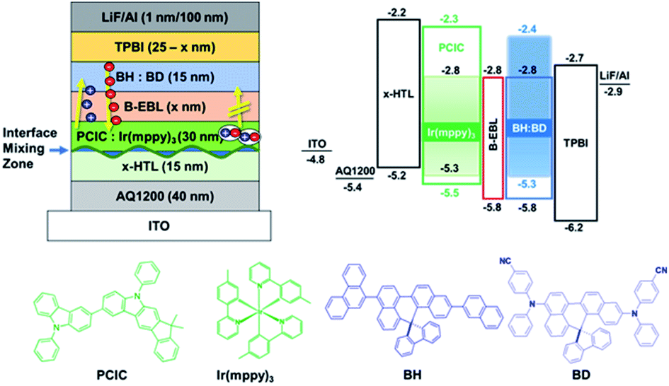
Organic light-emitting diodes (OLEDs) have been commercialized through vacuum thermal evaporation technology, but are still being developed to replace technologies related to solution processes such as inkjet printing technology that can reduce material consumption and create large-area products.1,2 For most solution processing devices, there are still many papers that design devices using phosphorescent materials. However, in order for a solution processed OLED device to be commercialized, problems such as efficiency and device lifetime must be solved. The main cause of this is that an annealing process is always added after the coating step. In this process, the phosphorescent dopant is separated from the host material, resulting in poor thermal stability. In fact, in a previous paper we reported that the red dopant escaped from the host at 150 °C.3 Phosphorescent devices are inherently affected by many triplet–triplet annihilation (TTA) or triplet-polaron quenching (TPQ) processes under high current density driving conditions, and these dopant agglomeration can be a major cause of reduced efficiency and lifetime.4,5 Apart from this problem, the mixing of the hole transport layer (HTL) and emitting layer (EML) interface suppresses the device lifetime. Especially, when an exciton is formed in this mixed region (HTL/EML), the material degradation may occur due to serious exciton-polaron quenching. Therefore, the material must be designed where the electrons do not approach this interface along with the EML, which means that the strong hole-transporting property in the EML could be more advantageous for improving efficiency. Therefore, in order to manufacture an efficient solution device, it is necessary to make a host material by appropriately utilizing carbazole in order to maintain a high triplet energy level (T1) while satisfying hole dominant conditions.6–8On the other hand, even if the blue light-emitting material forms a thin film by thermal evaporation technology, the lifetime is still short, so the long lifetime can't be guaranteed by the solution process. Therefore, a method of thermally evaporating blue EML as a common layer on the top patterned by a wet process such as ink-jet printing was introduced to overcome an issue of intrinsically short operational lifetime of blue OLED device which may show much shorter one if they are formed by solution process. In other words, to realize a blue common layer structure, we could print hole injection layer (HIL), HTL, red and green EML, and then use a thermal evaporation process to deposit a bipolar exciton blocking layer (B-EBL), blue EML, electron transport layer (ETL), electron injection layer (EIL), and cathode continuously. Among the many functional layers mentioned above, B-EBL plays an important role in inhibiting the triplet exciton energy of green or red dopant from being transmitted to the triplet state of the blue-light emitting layer to prevent blue light emission by TTA. Nevertheless, the performance of red and green devices manufactured by the solution process still shows poor performance compared to the thermal vacuum evaporation process. Hence, many reports have attempted to improve the performance of devices fabricated by solution processes. Here, we present a thermally stable device and a highly efficient solution-processed OLED with such a blue common layer structure.9–12
Experimental
Measurement and characterization of materials
The 1H and 13C nuclear magnetic resonance (NMR) were recorded on a Bruker 400 MHz (Bruker DPX) NMR spectrometer. Ultraviolet-visible (UV-vis) spectrophotometer (HP8453) and fluorescence spectrophotometer (Perkin Elmer LS50B) were used to measure UV-vis spectra and photoluminescence (PL) spectra. Low-temperature PL measurement of the synthesized materials was carried out at 77 K using a dilute solution of the materials. Cyclic voltammetry (CV) was measured by an Autolab/PGSTAT 2 model, which was equipped with a platinum 3 array type as the working electrode, platinum wire as the counter electrode, and Ag/0.1 M AgNO3 as the reference electrode, at room temperature in a solution of tetrabutyl-ammonium hexafluorophosphate (n-Bu4NPF6) (0.1 N) in acetonitrile under nitrogen gas protection, at a scan rate of 100 mV s−1. The differential scanning calorimeter (DSC) measurements were performed with a DSC2010 unit under a nitrogen flow at a heating rate of 10 °C min−1, from 30 °C to 300 °C. Thermogravimetric analysis (TGA) was conducted with a Thermogravimetric Analyzer S-1000 instrument under nitrogen with a heating rate of 10 °C min−1 from 30 °C to 700 °C. High-resolution mass spectra were recorded using a MALDI-TOF/TOFTF 5800 system (AB SCIEX) at the Korean Basic Science Institute (Seoul). The current density (J), voltage (V), and luminance (L) (J–V–L) properties obtained after the solution process were obtained using a Keithley SMU 2635A instrument, and the data for the luminance results were measured with a Minolta CS-100A instrument. In addition, the EL (Electroluminescence) spectrum and color coordinates of the green device (Commission International De'Eclairage (CIE), 1931) were measured using Minolta's CS-2000A spectroradiometer.Synthesis of 7,7-dimethyl-5-phenyl-2-(9-phenyl-9H-carbazol-3-yl)-5,7-dihydroindeno[2,1-b]carbazole (PCIC)
2-Bromo-7,7-dimethyl-5-phenyl-5,7-dihydroindeno[2,1-b]carbazole (15 g, 34.2 mmol), (9-phenyl-9H-carbazol-3-yl)boronic acid (11.79 g, 41.1 mmol), tetrakis(triphenylphosphine)-palladium(0) (1.58 g, 1.37 mmol), 2 M aqueous K2CO3 (34.47 mL, 68.9 mmol) in toluene![[thin space (1/6-em)]](https://www.rsc.org/images/entities/char_2009.gif) :EtOH:H2O (2:1:1 v/v/v%, 200 mL) was stirred, then keep it heating at 130 °C under N2 atmosphere for 12 h. The resulting mixture was cooled to room temperature and then filtered and washed CH2Cl2. After removal of the solvent by rotary evaporation, the residue was purified by silica gel column chromatography. Finally, PCIC was obtained as a white powder by train sublimation (yield 73%). 1H NMR (400 MHz, CDCl3) δ 8.55 (s, 1H), 8.54–8.48 (m, 2H), 8.26 (d, J = 7.7 Hz, 1H), 7.89 (d, J = 7.4 Hz, 1H), 7.81 (d, J = 6.6 Hz, 1H), 7.76 (d, J = 8.5 Hz, 1H), 7.68 (d, 4H), 7.64 (s, 4H), 7.56–7.47 (m, 4H), 7.44 (s, 4H), 7.39 (d, 1H), 7.34 (s, 1H), 7.30 (d, J = 7.8 Hz, 1H), 1.54 (s, 6H). 13C NMR (100 MHz, CDCl3) δ 153.51, 153.42, 141.89, 141.51, 140.68, 140.19, 139.89, 138.08, 137.96, 134.55, 132.56, 130.17, 130.07, 127.65, 127.60, 127.39, 127.25, 127.21, 126.42, 126.19, 125.99, 125.62, 124.37, 124.14, 123.75, 123.30, 122.68, 120.59, 120.13, 119.51, 119.04, 118.87, 111.59, 110.18, 110.05, 104.15, 46.94, 28.13. MALDI-TOF: calcd for C45H32N2, 600.2565; found 600.2485.
:EtOH:H2O (2:1:1 v/v/v%, 200 mL) was stirred, then keep it heating at 130 °C under N2 atmosphere for 12 h. The resulting mixture was cooled to room temperature and then filtered and washed CH2Cl2. After removal of the solvent by rotary evaporation, the residue was purified by silica gel column chromatography. Finally, PCIC was obtained as a white powder by train sublimation (yield 73%). 1H NMR (400 MHz, CDCl3) δ 8.55 (s, 1H), 8.54–8.48 (m, 2H), 8.26 (d, J = 7.7 Hz, 1H), 7.89 (d, J = 7.4 Hz, 1H), 7.81 (d, J = 6.6 Hz, 1H), 7.76 (d, J = 8.5 Hz, 1H), 7.68 (d, 4H), 7.64 (s, 4H), 7.56–7.47 (m, 4H), 7.44 (s, 4H), 7.39 (d, 1H), 7.34 (s, 1H), 7.30 (d, J = 7.8 Hz, 1H), 1.54 (s, 6H). 13C NMR (100 MHz, CDCl3) δ 153.51, 153.42, 141.89, 141.51, 140.68, 140.19, 139.89, 138.08, 137.96, 134.55, 132.56, 130.17, 130.07, 127.65, 127.60, 127.39, 127.25, 127.21, 126.42, 126.19, 125.99, 125.62, 124.37, 124.14, 123.75, 123.30, 122.68, 120.59, 120.13, 119.51, 119.04, 118.87, 111.59, 110.18, 110.05, 104.15, 46.94, 28.13. MALDI-TOF: calcd for C45H32N2, 600.2565; found 600.2485.
Materials
Plexcore® OC AQ1200 (AQ1200) purchased from Sigma-Aldrich was used as the HIL. And, HL-X026, a material for crosslinked hole transport layer (x-HTL) was supplied by Merck.13,14 In addition, a PCIC was doped with tris[2-(p-tolyl)pyridine] iridium(III) (Ir(mppy)3, green phosphorescent dopant) purchased from Lumtec.15 After the solution process of HIL, HTL, and EML, 11-(4,6-diphenyl-[1,3,5]-triazin-2-yl)-12-phenyl-11,12-dihydro-11,12-diaza-indenofluorene (DIC-TRZ) purchased from Lumtec was thermally evaporated as a bipolar exciton blocking layer (B-EBL). In addition, 10-(naphthalen-2-yl)-3-(phenanthren-9-yl)spiro[benzo[ij] tetraphene-7,9′-fluorene] (blue host, BH) and N6,N9-bis(4-cyanophenyl)-N3,N9-diphenylspiro[benzo[de]anthracene-7,9′-fluorene]-3,9-diamine (blue dopant, BD) supplied by Daejoo Electronic Materials Co., Ltd. were thermally evaporated for blue common layer (common EML).16 Then, finally, 2,2′,2′′-(1,3,5-phenylene)tris(1-phenyl-1H-benzimidazole) (TPBI, Sigma-Aldrich),17 lithium fluoride (LiF, Sigma-Aldrich) and aluminum (Al, Sigma-Aldrich) were successively deposited by thermal evaporation process.Device fabrication
The patterned indium tin oxide (ITO) glasses having a light emitting area of 3 × 3 mm2 used in the experiment was cleaned with acetone and isopropyl alcohol (IPA) for 10 minutes each with an ultrasonic cleaner. After that, the UV-ozone chamber was used for 20 minutes to increase the adhesion of the solution process and remove the remaining impurities, and the cleaning step was completed. First, we spin-coated AQ1200 on the ITO substrate as a HIL at 8000 rpm for 60 s. Then, they were annealed at 120 °C for 15 minutes in a glove box filled with a nitrogen. Subsequently, a crosslinkable hole transport material (x-HTM) was spin-coated on HIL at 3000 rpm for 30 s. Especially, it was crosslinked for 30 minutes at 220 °C in a pure nitrogen atmosphere. The HTL was reliably coated on top of the HIL despite the high temperature.18 After the formation of HIL and x-HTL, we formed EML as follows: To create a solution device for green phosphorescence; 1 wt% of PCIC solution, and 0.5 wt% of Ir(mppy)3 solution was prepared using toluene and chlorobenzene, respectively, as a solvent. The final EML solution having 5% of dopant mixed with PCIC, was spin-coated on HTL at 3000 rpm 30 s. Then, the device was finally annealed at 100 °C for 10 minutes.Result and discussion
Analysis of new synthetic green host material
We synthesized a new indenocarbazole derivative (PCIC), which could be used as a highly efficient host material for green phosphorescent OLEDs (PHOLEDs). The synthetic details are shown in Scheme 1. A PCIC was prepared via the well-known Suzuki–Miyaura aryl–aryl coupling reaction (C–C bond formation) in a high yield (∼84%). Very interestingly, an introduction of asymmetric molecular structure using indenocarbazole moiety could greatly improve the solubility of the material in common organic solvents such as chloroform, THF, toluene, xylene, and chlorobenzene, etc. Indeed, the solubility in toluene was greatly improved by more than 12 times compared to the typical and similar arylamine-based host material such as CBP (4,4′-bis(N-carbazolyl)-1,1′-biphenyl). We measured the solubility of this material in toluene and chlorobenzene and summarized in Table 1S (ESI†). This is very advantageous in making a high-quality film when manufacturing an OLED device by a solution process. The molecular structure of PCIC was confirmed by 1H and 13C NMR spectroscopy and MALDI-TOF mass spectrometry. The detailed spectral data for the determination of the molecular structure were shown in Fig. 1S–3S.† Besides, the electrochemical properties and thermal behavior of the synthetic hosts were also shown in Fig. 4S–6S in the ESI.† | ||
| Scheme 1 Syntheses of PCIC. | ||
To understand the molecular geometry of the ground and the excited state of the new synthetic host material (PCIC), we carried out a molecular simulation following density functional theory (DFT) with the Schrödinger Materials Science program (version 4.1). We also proceeded with a time-dependent DFT (TD-DFT) calculation to obtain singlet energy level (S1) and triplet energy level (T1) of an optimized geometry of the host molecule.19 The theory and basis set we applied for all calculations was B3LYP/6-31G (d,p). Looking at the PCIC from the side of the geometry optimized structure, it can be seen that the indenocarbazole moiety and carbazole moiety are bent with a dihedral angle of about 42°.
This structure has a slightly smaller dihedral angle compared to the previously developed materials, but it was judged that additionally introduced methyl groups and phenyl groups hindered the stacking or ordering of molecules, indicating that they would be suitable for the solution process.20 Looking at the electron cloud distributions of HOMO and LUMO predicted from molecular simulation, it was confirmed that the electron cloud bands of HOMO spread widely along the two carbazoles, and then converge to one side in LUMO as shown in Fig. 1. The calculated HOMO and LUMO energy levels estimated from the corresponding optimized molecular geometry were −5.53 eV and −2.34 eV, respectively, and T1 was estimated to be 2.76 eV. In addition, some electronic properties of PCIC material were measured experimentally (Fig. 4S†). From absorption edge analysis, the Eg of 3.18 eV was obtained, and the HOMO level of 5.48 eV was estimated by cyclic voltammetry. From those data, the LUMO level was calculated as 2.3 eV. Meanwhile, from the photoluminescence (PL) spectrum, we estimated a T1 energy level. In other words, the T1 energy level of PCIC measured at low temperature (77 K) was determined to be 2.75 eV (Fig. 2). However, according to a recent report by Lee et al., the phosphorescent dopant can be quasi-dewet from EML and escape during annealing procedure during solution processes if the thermal stability of the host materials is very low.3 To confirm such a possibility, we proceeded with differential scanning calorimetry (DSC) analysis of the PCIC material and, in the end, confirmed that the glass transition temperature (Tg) is very low, about 98 °C, and the Tm is about 234 °C (Table 1). So, we performed molecular dynamics simulation to predict how the relative distance between molecules can be changed on series of annealing processes. However, we simulated the molecular stacking or ordering behavior by using imaginary spaces filled with PCIC materials mixed with green dopant molecules (Ir(mppy)3, 5 mol%) after the annealing process (Fig. 3).
 | ||
| Fig. 1 HOMO, LUMO distributions and energy level of PCIC predicted through DFT and TD-DFT calculations. | ||
| Host | λabs (nm) | λPL (nm) | EHOMOb (eV) | ELUMOc (eV) | Eoptgc (eV) | Etd (eV) | Tge (°C) | Tme (°C) | Tdf (°C) | ||
|---|---|---|---|---|---|---|---|---|---|---|---|
| Sola | Film | Sola | Film | ||||||||
| a Toluene solution (1.0 × 10⁻⁵ M).b Measured by cyclic voltammetry.c Estimated from the absorption spectra threshold.d Estimated from the phosphorescence spectra in toluene at 77 K.e Estimated from DSC measurements.f Estimated from TGA measurements corresponding to 5% weight loss. | |||||||||||
| PCIC | 318 | 318 | 387, 407 | 395, 415 | −5.48 | −2.30 | 3.18 | 2.75 | 98 | 234 | 482 |
 | ||
| Fig. 2 UV-visible absorption and photoluminescence (PL) spectra of PCIC. | ||
For molecular dynamics simulation, we created a tangled chain type unit cell containing a total of 226 molecules (10 Ir(mppy)3 and 216 PCIC molecules) by performing the Disordered System Builder mode with OPLS3e force filed applied.21 Then, molecular dynamics (MD) simulation to reach the equilibrium system with 10.0 ns and NPT conditions as well as the MD protocols (relaxation protocol) of three stage conditions was performed.22 Next, simulations were performed with 50.0 ns and NPT conditions at 100 °C, 120 °C, and 140 °C to see the annealing effect, and finally MD simulations were performed under 10.0 ns and 300 K conditions (Fig. 3(left)). Then, the value of g(r) was calculated as the probability of finding a molecule within the distance r through radial distribution functions (RDF) simulation. The calculated data are shown in Fig. 3(right).
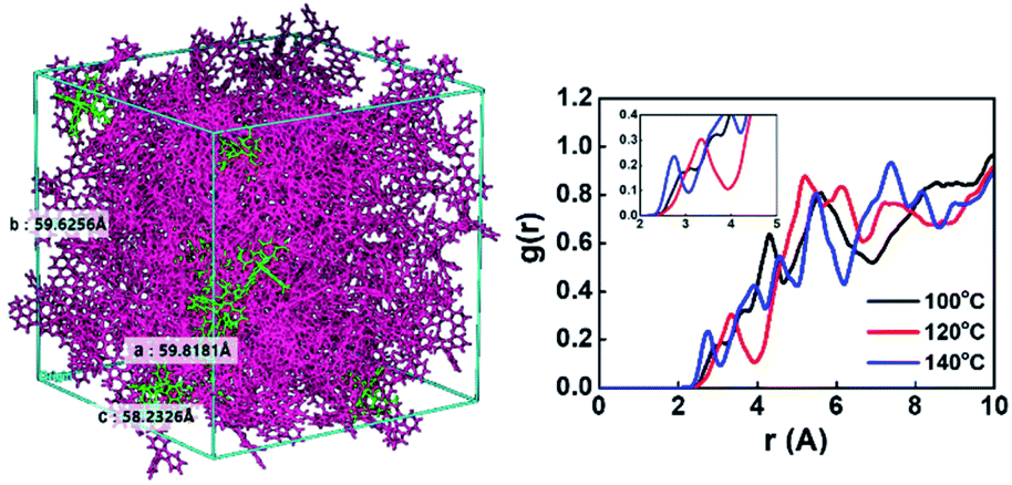 | ||
| Fig. 3 Molecular structure containing PCIC and 5 mol% of Ir(mppy)3 in a unit cell (left), radial distribution functions (RDFs) calculated by simulation method (right). | ||
Very interestingly, the intermolecular distance decreased from 3.3 Å to 2.7 Å as the temperature increased from 120 °C to 140 °C. In other words, when the annealing temperature of PCIC materials is increased, the distance between molecules does not increase, but rather gets closer, which means that PCIC molecules have less chance of segmental motion. By analogy with these facts, it means that PCIC materials do not cause severe segmental motion. We also performed AFM analysis to identify the surface roughness of synthetic PCIC film as well as the film composed of PCIC doped with 5 mol% of Ir(mppy)3. First, the average roughness (Ra), peak to valley height (Rpv), root mean square roughness (Rq) values of the pure PCIC surface were measured as 0.42, 4.19, and 0.52 nm, respectively. In addition, Ra, Rpv, and Rq were measured as 0.27, 3.67, and 0.35 nm, respectively, from the thin film of PCIC doped with 5 mol% of Ir(mppy)3. From these results, we confirmed the PCIC molecule, as well as PCIC doped with 5 mol% of Ir(mppy)3, is a good approach for the solution process device (Fig. 4 and Table 2).
 | ||
| Fig. 4 AFM images of EML surfaces (a) PCIC (30 nm), (b) PCIC:Ir(mppy)3 (5 mol%, 30 nm). | ||
| Film | Ra (nm) | Rpv (nm) | Rq(nm) |
|---|---|---|---|
| PCIC | 0.42 | 4.19 | 0.52 |
| PCIC:Ir(mppy)3 (5 mol%) | 0.27 | 3.67 | 0.35 |
Device characteristics
It is very important to implement a multi-layered structure to improve the efficiency and lifetime of the solution device. Since the first layer, the hole injection layer (HIL), contains a lot of water-soluble substances, coating the second layer, HTL, is not a big problem. However, in order to coat EML on HTL, the HTL must not be washed away during spin coating of the EML solution. Therefore, we formed crosslinked HTL (x-HTL) by using Merck's crosslikable HTM (HL-X026).13,23 A new synthetic PCIC material mixed with 5 mol% Ir(mppy)3 was spin coated on this layer. The resulting device structure is shown in Fig. 5. As mentioned earlier, the interface that is of great concern in manufacturing the solution device is the interface between x-HTL and EML, and even if the HTL is crosslinked, some interface mixing occurs, and chemical instability occurs due to exciton-polaron quenching. Therefore, the molecular selection to bias the exciton formation zone toward the ETL is very important. To form an exciton formation zone at such interface, we introduced TPBI having relatively low electron mobility (∼10−5 cm2 V−1 s−1). | ||
| Fig. 5 Energy band diagram of the green phosphorescence OLEDs. | ||
Fig. 6(a) shows the J–V–L characteristics of green solution process OLEDs. The turn-on voltage (Von) at a constant luminance of 1 cd m−2 was 3.5 V for device A. The driving voltage (Vop) obtained at a luminance of 1000 cd m−2 was 6.5 V for device A. Likewise, the current density at 6.0 V was 0.82 mA cm−2 for device A. Meanwhile, at a constant luminance of 1000 cd m−2, the current efficiency was recorded to 55.2 cd A−1 for device A (Fig. 6(b)). Besides, the maximum current efficiency was 55.4 cd A−1 for device A in Table 3. The peak wavelength of the EL spectrum of the resulting device was 512 nm as shown in Fig. 6(c). Although we recorded high values in terms of efficiency, operational stability (Fig. 6(d)), the best half-life obtained here is only 5.0 hours for device A. As a solution device, the efficiency was quite high, but device A had a relatively low operational stability and a lifetime of only 5 hours, so we recognized that device optimization is required.24
 | ||
| Fig. 6 (a) J–V–L curves, (b) current efficiency, (c) EL spectra property, and (d) operational lifetime characteristics of PHOLEDs. | ||
Therefore, in order to overcome the low driving performance of green phosphorescent device (device A) manufactured by the solution process, we used a blue common layer approach that can more effectively limit the inflow of electrons and move the exciton formation region away from the interface mixing zone. Even if the blue common layer is deposited as a common layer on the top, electrons passing through the blue light-emitting layer on the top must be quickly transferred to green in order to emit light only from the wet-processed green emitter on the bottom. The holes through the lower green layer should enter very limitedly into the blue light-emitting layer. Since the layer that can perform this function is B-EBL, and B-EBL has a role to prevent migration of the triplet exciton made in the lower green emission layer to the blue emission layer, too. Thus, the bipolar materials with high T1 should be selected. The reason for this is as follows: if energy corresponding to T1 of the under-lying phosphorescent green is transferred to the T1 state of the blue light-emitting material on the top due to its low T1, side light emission may occur in the blue light emitter through the TTA process inside blue light emitting layer. Thus, we inserted a bipolar exciton blocking layer (B-EBL) with a high T1 energy level (DIC-TRZ, T1 = 2.82 eV)25 between the green emitter and the blue emitter to suppress the migration of green exciton to the adjacent blue layer as shown in the top left part in Fig. 7.
 | ||
| Fig. 7 Energy band diagram of the green phosphorescence OLEDs with blue common layer structure. | ||
Therefore, we first tried to optimize the thickness of B-EBL and ETL because they are the most important layers to realize the blue common layer approach. For this experiment, in order to maintain the total electric field applied to the entire device, the total thickness of B-EBL, BCL, and ETL was kept at 40 nm. The detailed configuration of the devices fabricated is as follows:
ITO/AQ1200/x-HTL/PCIC:Ir(mppy)3 (5 mol%)/B-EBL (x nm)/BH:BD/TPBI (25–x nm)/LiF/Al (where x = 3, 5, 7 nm for devices B, C and D) (device configurations, including thickness conditions, are given in ESI†).
Fig. 8(a) shows the J–V–L characteristics of green solution process OLEDs. The turn-on voltages (Von) at a constant luminance of 1 cd m−2 were 4.5 V for devices B, C and D. The driving voltages (Vop) obtained at a luminance of 1000 cd m−2 were 8.6 V, 7.9 V, and 7.8 V for devices B, C and D, respectively. Likewise, the current density at 6.0 V was 0.13 mA cm−2 for device B, 0.15 mA cm−2 for device C and 0.22 mA cm−2 for device D, respectively. Although the thickness of B-EBL increased from 3 nm to 7 nm, it can be seen that the amount of current reaching the EML increases as the thickness of TPBI decreases from 22 nm to 18 nm. This might be due to the higher electron mobility of B-EBL (2.5 × 10⁻³ cm2 V−1 s−1) than TPBI (∼10−5 cm2 V−1 s−1) so that the recombination region more influences the thickness change of TPBI. In other words, the driving voltage gradually decreases as the thickness of TPBI, which has low mobility, decreases. More specifically, at a constant luminance of 1000 cd m−2, the current efficiency was recorded to 53.6 cd A−1 for device B, 60.3 cd A−1 for device C and 56.7 cd A−1 for device D, respectively (Fig. 8(b)). Besides, the maximum current efficiency was 53.7 cd A−1 for device B, 60.3 cd A−1 for device C and 60.9 cd A−1 for device D, respectively, as summarized in Table 4. The EL spectra of the three devices were obtained identically as shown in Fig. 8(c), despite the different conditions of the part corresponding to the ETL side. In conclusion, it was confirmed that when the B-EBL is 3 nm, the efficiency and driving voltage characteristics are inferior. On the other hand, when the B-EBL is increased to 7 nm, the driving voltage is rather lowered, but the efficiency is somewhat reduced. Therefore, the 5 nm condition for the B-EBL was judged to be the most suitable condition for this BCL approach. In other words, if we use about 5 nm of DIC-TRZ material (B-EBL) and about 20 nm of TPBI, electrons are supplied to the green EML coated on the bottom without any problem, resulting in efficient light emission.
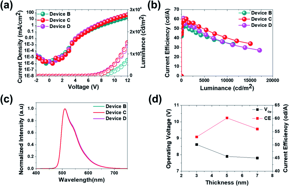 | ||
| Fig. 8 (a) J–V–L curves, (b) current efficiency (CE) and luminance results, (c) EL spectra property, and (d) dependence of operating voltage and CE on the thickness of B-EBL at 1000 cd m−2. | ||
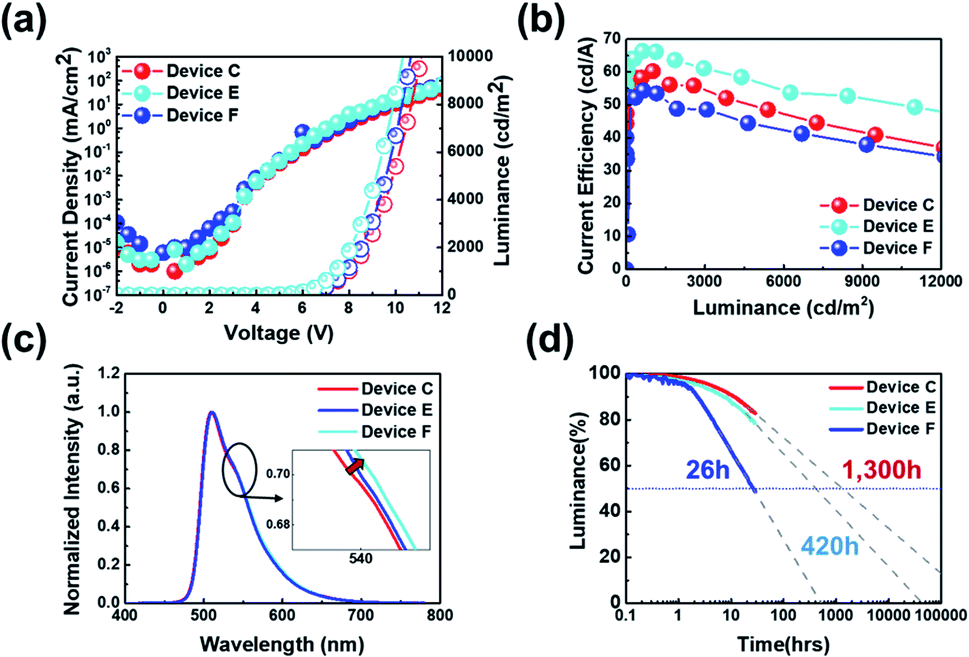
Therefore, we selected the thickness that fits the conditions of device C on the top of the EML and optimized the thickness of the materials on the bottom of the EML. In other words, for this experiment, the control device was manufactured in the structure of device C. Besides, device E and device F were additionally prepared as follows:
ITO/AQ1200/x-HTL/PCIC:Ir(mppy)3 (5 mol%)/B-EBL/BH:BD/TPBI/LiF/Al (where thickness of AQ1200 and x-HTL: 30 nm and 25 nm for device E; 20 nm and 35 nm for device F) (device configurations, including thickness conditions, are given in ESI†).
The J–V–L characteristics of those fabricated devices (devices C, E and F) were shown in Fig. 9(a). The Von at a constant luminance of 1 cd m−2 were measured to 4.5 V for devices C, E and F. And the Vop obtained at a luminance of 1000 cd m−2 were 7.9 V, 7.8 V and 7.4 V for devices C, E and F, respectively. Likewise, the current density at 6.0 V was 0.22 mA cm−2 for device C, 0.67 mA cm−2 for device E, and 0.15 mA cm−2 for device F, respectively. As mentioned earlier, the current density tended to diminish as the ETL thickness decreases. However, we found that J does not decrease according to the increase in HTL thickness. The J was increased from 0.15 mA cm−2 to 0.67 mA cm−2 when the thickness of HTL was changed from 15 nm to 25 nm. This might be due to a shift of the recombination zone toward the central region of EML (device F) from the ETL side (device C). However, J decreased rapidly when the thickness of the HTL increased to 35 nm presumably due to an additional shift of recombination zone toward the HTL side, which is an interface mixing zone. Meanwhile, at a constant luminance of 1000 cd m−2, the current efficiency was recorded to 60.3 cd A−1 for device C, 66.2 cd A−1 for device E and 53.5 cd A−1 for device F, respectively. This can be said to be consistent with the analogy of the change according to the movement of the recombination zone mentioned above. Besides, the maximum current efficiency values were measured as 60.3 cd A−1 for device C, 66.4 cd A−1 for device E and 54.4 cd A−1 for device F, respectively, as summarized in Table 5. Meanwhile, a different trend was observed in the operational stability (Fig. 9(d)), the best half-lifetime we obtained here is 1300 hours for device C, while the half-lifetime for device E and device F is 420 hours and 26 hours, respectively. A very interesting fact is also shown in Fig. 9(c). In other words, as the thickness of HTL increases from device C to device E or device F, it can be seen that the secondary peak intensity of the EL spectrum is increasing. This change is the optical effect caused by the recombination zone shift. Indeed, it is well-known that as the secondary peak intensity increases, the recombination zone gets closer to the HTL (Fig. 9).26
 | ||
| Fig. 9 (a) Current density–voltage–luminance, (b) current efficiency–luminance, (c) electroluminescence, and (d) operational lifetime characteristics of hybrid PHOLEDs with different HTL and HIL thickness. | ||
To find out why there is a difference between the conditions of high efficiency and long lifetime, we prepared hole only devices (HOD) and electron only devices (EOD) as shown in Fig. 10. The detailed configuration of the devices fabricated is as follows:
 | ||
| Fig. 10 (a) HOD and EOD energy diagram consisting of pure PCIC and PCIC:Ir(mppy)3 (5 mol%), (b) J–V characteristics of HOD A, HOD B, EOD A and EOD B, (c) data results of J (HOD A)/J (EOD A) and J (HOD B)/J (EOD B) (device configuration with a thickness information is shown in the ESI†). | ||
ITO/PEDOT:PSS/PCIC (HOD A) & PCIC:Ir(mppy)3 (5 mol%, HOD B)/MoO3/Al.
ITO/ZnO/PEI/PCIC (EOD A) & PCIC:Ir(mppy)3 (5 mol%, EOD B)/Al.
Considering the electrical energy characteristics of PCIC, the energy levels of HOMO and LUMO are shallow, so it is expected that the injection of holes is basically easier than the injection of electrons. We fabricated two HODs and two EODs devices to more accurately find out this characteristic. The difference in HOMO energy level between PCIC and Ir(mppy)3 is only 0.2 eV, but since the hole cannot be injected only into the host and can be trapped by the dopant, the hole current density is reduced by about 1 order of magnitude by doping. On the other hand, although the LUMO energy level of PCIC is too shallow, the difference in LUMO energy from the dopant remains as much as 0.5 eV, but the decrease in current density due to electron trapping was not observed significantly. As a result, the host material itself is expected to have a hole mobility value of about 60 times greater than that of electron mobility, but in the case of a doped device, the hole mobility value is expected to be about 2 times greater than that of electron mobility (Fig. 10).
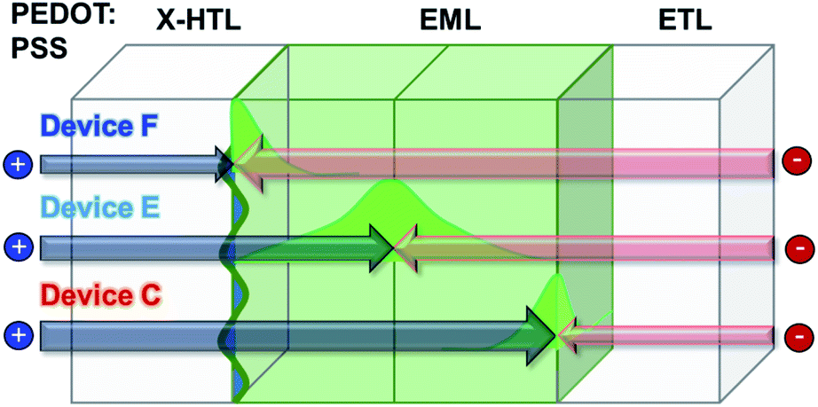
Therefore, when the thickness of the X-HTL is thin, the resistance of the cross-linked X-HTL is relatively small, and the recombination zone can be skewed toward the B-EBL, and the area can become very narrow so that the efficiency decreases (device C). On the other hand, if we can move it toward the HTL side, the recombination zone can be widened and the efficiency can be increased. In fact, the efficiency was the highest under the conditions of device E. But, the efficiency decreased again in device F. However, unlike efficiency, in the case of a lifetime, it was found that device C, which has the recombination zone furthest from the HTL and EML interface mixing zone, is the most advantageous for operational stability (e.g. device lifetime). This fact has been proven in several previously published papers,27–29 and it can be seen that the trend is in good agreement with such previous results. Fig. 11 shows a schematic diagram of the location according to the recombination zone.
 | ||
| Fig. 11 Location of the exciton recombination zone of green PHOLED. | ||
In general, a hole-transporting host materials are known to have very low anionic state stability, so the lifetime of device E and device F, where electrons reach deeper, is a disadvantage. To find out the actual bond dissociation energy (BDE) value of PCIC, the molecular simulation was performed and summarized in Table 6 (Fig. 12).
| Area | Neutral | Anion | Cation |
|---|---|---|---|
| 1 | 3.59 | 1.20 | 3.65 |
| 3.15 | 5.84 | ||
| 2 | 3.65 | 1.37 | 3.83 |
| 3.21 | 5.91 |
We confirmed that the anion state of PCIC is very weak through the BDE calculation result, whereas the cation state has a relatively strong bond (Table 6). In the case of device F, as electrons move toward the HTL and EML interface, the width of electrons exposed to the host increases. Therefore, deterioration occurs due to the weak anion state, resulting in reduced efficiency and lifetime. However, for device C, the thin HTL thickness results in the formation of recombination zone at the EML and B-EBL interfaces. The relatively strong cation state is stable against deterioration and so, in the case of device C, the lifetime characteristic is 50 times higher than that of device F, and it showed a stable characteristic. In fact, as mentioned earlier, due to the shallow LUMO of PCIC and the deep electron trapping level of the green dopant, it will be possible to keep the recombination zone close to the B-EBL side, and we expect that there will be room for further improvement in a lifetime.
 | ||
| Fig. 12 Area where bond breaks in PCIC structure. | ||
Conclusions
To manufacture green phosphorescent OLED with a blue common layer structure, a new host material (PCIC) with excellent hole transportability was rationally designed and synthesized. But, we found that the bond dissociation energy of the anionic state of this host material is too low (∼1.4 eV) to be used as an EML material. Thus, we used an Ir(mppy)3 having a deep electron trapping energy level to cause a direct charge trapping emission at the interface between EML and B-EBL30 thereby lowering the possibility of host material dissociation. From this approach, we could realize very good lifetime behaviour of the green PHOLEDs with a blue common layer structure, while we obtained high-efficiency characteristics when the recombination zone is positioned at the centre of EML. Because of this, high efficiency can be recorded when recombination regions are generated in EML, but in order to maximize lifetime with stable properties, we need to move the exciton formation zone to the EML and B-EBL interfaces to inhibit bond dissociation. This novel study is very useful for making long lifetime s-OLEDs devices.Conflicts of interest
The authors declare no competing financial interest.Acknowledgements
This work was supported by the Industrial Strategic Technology Development Program (20011059, Development of inks for emitting layers with high performance and long lifetime) and the Technology Innovation Program (20010443, Development of mass spectrometry for OLED structure and stability analysis) funded by the Ministry of Trade, Industry & Energy (MOTIE, Korea). This work was also supported by Basic Science Research Program through the National Research Foundation of Korea (NRF) funded by the Ministry of Education (2021R1A2C1008725). Finally, this work was sponsored by BK21 FOUR Program funded by the Ministry of Education (MOE, Korea) and National Research Foundation of Korea (NRF) (21A20130000018).References
- H. Sirringhaus, T. Kawase, R. H. Friend, T. Shimoda, M. Inbasekaran, W. Wu and E. P. Woo, High Resolution Inkjet Printing of All-Polymer Transistor Circuits, Science, 2000, 290, 2123–2126 CrossRef CAS PubMed.
- R. A. Street, W. S. Wong, S. E. Ready, M. L. Chabinyc, A. C. Arias, S. Limb, A. Salleo and R. Lujan, Jet Printing Flexible Displays, Mater. Today, 2006, 9, 32–37 CrossRef CAS.
- J. Y. Lee, J. Kim, H. Kim and M. C. Suh, Molecular Stacking Effect on Small-Molecular Organic Light Emitting Diodes Prepared with Solution Process, ACS Appl. Mater. Interfaces, 2020, 12, 23244–23251 CrossRef CAS PubMed.
- S. Lamansky, R. C. Kwong, M. Nugent, P. I. Djurovich and M. E. Thompson, Molecularly Doped Polymer Light Emitting Diodes Utilizing Phosphorescent Pt(II) and Ir(III) Dopants, Org. Electron., 2001, 2, 53–62 CrossRef CAS.
- L. Duan, L. Hou, T.-W. Lee, J. Qiao, D. Zhang, G. Dong, L. Wang and Y. Qiu, Solution Processable Small Molecules for Organic Light-Emitting Diodes, J. Mater. Chem., 2010, 20, 6392–6407 RSC.
- H. Kim, Y. Byun, R. R. Das, B. K. Choi and P.-S. Ahn, Small Molecule Based and Solution Processed Highly Efficient Red Electrophosphorescent Organic Light Emitting Devices, Appl. Phys. Lett., 2007, 91, 093512 CrossRef.
- S. H. Cho and M. C. Suh, An Enhanced Operational Stability of Organic Light Emitting Devices with Polymeric Buffer Layer, Jpn. J. Appl. Phys., 2012, 51, 041601 CrossRef.
- H. S. Jeon, S. H. Cho, J. Seo, Y. Park and M. C. Suh, Operation Voltage Behavior of Organic Light Emitting Diodes with Polymeric Buffer Layers Doped by Weak Electron Acceptor, Thin Solid Films, 2013, 546, 176–179 CrossRef CAS.
- Y.-H. Niu, M. S. Liu, J.-W. Ka, J. Bardeker, M. T. Zin, R. Schofield, Y. Chi and K.-Y. Jen, Crosslinkable Hole-Transport Layer on Conducting Polymer for High-Efficiency White Polymer Light-Emitting Diodes, Adv. Mater., 2007, 19, 300–304 CrossRef CAS.
- Y. R. Cho, H. S. Kim, Y. J. Yu and M. C. Suh, Highly Efficient Organic Light Emitting Diodes Formed by Solution Processed Red Emitters with Evaporated Blue Common Layer Structure, Sci. Rep., 2015, 5, 15903 CrossRef CAS PubMed.
- H. Y. Shin and M. C. Suh, A Study on Full Color Organic Light Emitting Diodes with Blue Common Layer under the Patterned Emission Layer, Org. Electron., 2014, 15, 2932–2941 CrossRef CAS.
- T. Matsumoto, T. Yoshinaga, T. Higo, T. Imai, T. Hirano and T. Saaoka, High-Performance Solution Processed OLED Enhanced by Evaporated Common Layer, J. Soc. Inf. Disp., 2011, 42, 924–927 CAS.
- W. Park, S. C. Yoon and J. Lee, Comparison of Optical and Electrical Properties of Different Hole-Transporting Materials for Solution-Processable Organic Light-Emitting Diodes, J. Nanosci. Nanotechnol., 2019, 19, 4578–4582 CrossRef CAS PubMed.
- S.-R. Park, D. H. Shin, S.-M. Park and M. C. Suh, Benzoquinoline-based Fluoranthene Derivatives as Electron Transport Materials for Solution-Processed Red Phosphorescent Organic Light-Emitting Diodes, RSC Adv., 2017, 7, 28520–28526 RSC.
- M. C. Suh, B. Pyo and H. S. Kim, Suppression of the Viewing Angle Dependence by Introduction of Nanoporous Diffuser Film on Blue OLEDs with Strong Microcavity Effect, Org. Electron., 2016, 28, 31 CrossRef CAS.
- J. H. Jeon, S. J. Cha, Y. M. Jeon, J.-H. Lee and M. C. Suh, Thermal Buffer Materials for Enhancement of Device Performance of Organic Light Emitting Diodes Fabricated by Laser Imaging Process, Org. Electron., 2014, 15, 2802–2809 CrossRef CAS.
- Y. Li, B.-X. Li, W.-Y. Tan, Y. Liu, X.-H. Zhu, F.-Y. Xie, J. Chen, D.-G. Ma, J. Peng, Y. Cao and J. Roncali, Structure-Properties Relationships in Solution-Processable Single Material Molecular Emitters for Efficient Green Organic Light-Emitting Diodes, Org. Electron., 2012, 13, 1092–1099 CrossRef CAS.
- J. Zhou, D. H. Anjum, L. Chen, X. Xu, I. A. Ventura, L. Jiang and G. Lubineau, The Temperature-Dependent Microstructure of PEDOT/PSS Films: Insights from Morphological, Mechanical and Electrical Analyses, J. Mater. Chem. C, 2014, 2, 9903–9910 RSC.
- E. Runge and E. K. U. Gross, Density-Functional Theory for Time-Dependent Systems, Phys. Rev. Lett., 1984, 52, 997–1000 CrossRef CAS.
- M. C. Suh, S.-R. Park, Y. R. Cho, P.-G Kang, D. A. Ahn, H. S. Kim and C.-B. Kim, Synthesis of Soluble Host Materials for Highly Efficient Red Phosphorescent Organic Light-Emitting Diodes, ACS Appl. Mater. Interfaces, 2016, 8, 18256–18265 CrossRef CAS PubMed.
- K. Roos, C. Wu, W. Damm, M. Reboul, J. M. Stevenson, C. Lu, M. K. Dahlgen, S. Mondal, W. Chen, C. Wang, R. Abel, R. A. Friesner and E. D. Harder, OPLS3e: Extending Force Field Coverage for Drug-Like Small Molecules, J. Chem. Theory Comput., 2019, 15, 1863–1874 CrossRef CAS PubMed.
- D. E. Shaw Research, Desmond Molecular Dynamics System, New York, NY, 2019 Search PubMed.
- F.-E. Meyer, N. Schulte, R. P. Scheurich, R. M. Anémian, A. Ludemann and A. Julliart, Cross-linkable and Cross-linked Polymer, Methods for the Production Thereof, and Use Thereof, Merck Patent GmbH, EP2401315B1, European Patent Office, 10-2014-7032101, filed April 12, 2013 and issued January 21, 2015 Search PubMed.
- K. S. Yook and J. Y. Lee, Small Molecule Host Materials for Solution Processed Phosphorescent Organic Light-Emitting Diodes, Adv. Mater., 2014, 26, 4218–4233 CrossRef CAS PubMed.
- D. Zhang, L. Duan, C. Li, Y. Li, H. Li, D. Zhang and Y. Qiu, High-Efficiency Fluorescent Organic Light-Emitting Devices Using Sensitizing Hosts with a Small Singlet–Triplet Exchange Energy, Adv. Mater., 2014, 26, 5050–5055 CrossRef CAS PubMed.
- J. Lee, J.-I. Lee, J. Y. Lee and H. Y. Chu, Stable Efficiency Roll-Off in Blue Phosphorescent Organic Light-Emitting Diodes by Host Layer Engineering, Org. Electron., 2009, 10, 1529–1533 CrossRef CAS.
- J. Fu, C. Chen, C. Shi and D. Ma, Solution-Processed Small Molecules As Mixed Host for Highly Efficient Blue and White Phosphorescent Organic Light-Emitting Diodes, ACS Appl. Mater. Interfaces, 2012, 9, 6579–6586 CrossRef PubMed.
- D. A. Ahn, S. Lee, J. Chung, Y. Park and M. C. Suh, Impact of Interface Mixing on the Performance of Solution Processed Organic Light Emitting Diodes—Impedance and Ultraviolet Photoelectron Spectroscopy Study, ACS Appl. Mater. Interfaces, 2017, 9, 22748–22756 CrossRef CAS PubMed.
- S.-R. Park, J.-H. Kang, D. A. Ahn and M. C. Suh, A Cross-Linkable Hole Transport Material Having Improved Mobility through a Semi-Interpenetrating Polymer Network Approach for Solution-Processed Green PHOLEDs, J. Mater. Chem., 2018, 6, 7750–7758 RSC.
- R. A. K. Yadav, D. K. Dubey, S.-Z. Chen, T.-W. Liang and J.-H. Jou, Role of Molecular Orbital Energy Levels in OLED Performance, Sci. Rep., 2020, 10, 9915 CrossRef CAS PubMed.
Footnote |
| † Electronic supplementary information (ESI) available. See DOI: 10.1039/d1ra04855d |
| This journal is © The Royal Society of Chemistry 2021 |