DOI:
10.1039/D1RA04663B
(Paper)
RSC Adv., 2021,
11, 28326-28331
Self-catalyst β-Ga2O3 semiconductor lateral nanowire networks synthesis on the insulating substrate for deep ultraviolet photodetectors†
Received
16th June 2021
, Accepted 16th August 2021
First published on 20th August 2021
Abstract
Monoclinic gallium oxide (β-Ga2O3) is a super-wide bandgap semiconductor with excellent chemical and thermal stability, which is an ideal candidate for detecting deep ultraviolet (DUV) radiation (100–280 nm). The growth of β-Ga2O3 is challenging and most methods require Au as the catalyst and a long reacting time (more than 1 hour). In this work, the self-catalyst β-Ga2O3 lateral nanowire networks were synthesized on an insulating substrate rapidly by a simple low-cost Chemical Vapor Deposition (CVD) method. A thin film of β-Ga2O3 nanowire networks was synthesized within a reacting time of 15 minutes, which possesses a huge possibility for the rapid growth of β-Ga2O3 metal oxide nanowires networks and application in the future solar-blind photodetector. MSM (metal–semiconductor–metal) photodetectors based on the β-Ga2O3 nanowire networks revealed fast response (on–off ratios is about 103), which is attributed to the unique cross-junction barrier-dominated conductance of the nanowire networks. In addition, the self-catalyst β-Ga2O3 nanowires grown on insulating SiO2 are achieved and could be expected to find important applications in a bottom-up way of fabricating the next generation semiconductor nanoelectronics.
Introduction
Solar-blind deep ultraviolet (DUV) photodetectors, sensitive to a spectrum range from 200 to 280 nm,1,2 have drawn considerable attention due to their wide applications in commercial and military fields, including flame or engine monitoring, missile warning, chemical or biological agent sensing and ultraviolet (UV) astronomy.3–8 Compared with thin-film counterparts, high-quality 1D nanostructures that usually have a high specific surface area would raise the density of surface trap states. Also, the low dimensionality could strongly confine the charge carriers, which provide high responsivity and photoconductive gain in nanoscale photodetectors.9 Inspired by these ideas, various UV light detectors based on 1D semiconductor structures have been fabricated.10–14
Monoclinic gallium oxide (β-Ga2O3) is a super-wide bandgap semiconductor (4.9 eV) material with excellent chemical and thermal stability, which is an ideal candidate for detecting deep ultraviolet (DUV) radiation (200–280 nm).15 Many works on the optoelectronic properties of β-Ga2O3 single crystal, film and planar heterojunctions have been carried out.16–23 Their excellent photoelectric properties prove the promising applications of gallium oxide in deep UV detection. Over the last few decades, 1D nanomaterials have attracted intensive fascinating both fundamental science and potential applications in future nanoscale electronics, optoelectronics and sensing devices. Their unique geometry offers fascinating and novel physical properties. Several DUV photodetectors based on β-Ga2O3 in either thin films or nanostructures have been successfully developed.24–32 In particular, benefiting from quantum confinement effect and remarkable surface/size effect, β-Ga2O3 nanostructures, mainly 1D β-Ga2O3 nanowires (NWs) nanobelts (NBs), can exhibit attractive merits of better optical absorption, improved charge carrier counterpart.33–38 Therefore, significant progress has been made in the growth of high-quality β-Ga2O3 NWs/NBs for DUV photodetectors' application. Due to a large surface-to-volume ratio and a Debye length comparable to the small size, they demonstrate superior sensitivity to surface processes. Besides, their size confinement renders a tunable bandgap, higher optical gain and faster operation speed.39–43 Furthermore, the catalysts, such as Au, Pt, Sn, etc., as precious metals catalysts, are usually used in the semiconductor oxide nanowires synthesis process. These catalysts are too expensive and will take metal contamination to the synthesis process. A simple self-catalyst or without-catalyst semiconductor nanowires synthesis process development is necessary. And also, this self-catalyst synthesis method is conducive to promoting process, which the metal-oxide semiconductor nanowires synthesized on the insulator SiO2 surface to form semiconductor–insulator nanostructure.44,45
This paper proposes a simple and low-cost method of growing the self-catalyst ultra-long β-Ga2O3 nanowire networks on SiO2 insulating substrate using chemical vapor deposition (CVD). Self-catalyst reaction refers to a type of reaction in which the reactant itself has a catalytic effect and can accelerate or slow down the progress of the reaction. Here, Ga metal's catalyst is from reducing the nutrient of β-Ga2O3 at the beginning of the synthesis process. In general, the experiments were carried out with the sources of reducing carbon agent that the only commonly used carbon is graphite, which requires a higher heating temperature for thermal reducing and vaporizing the source. Because of all, nano-diamond was used as carbon sources in this work. Compared with other carbon sources, the reaction of nano-diamond as a raw material can reduce the reaction temperature and enhance the intensity of the reaction.46,47 The response and recovery time of the β-Ga2O3 nanowire networks photodetector device under 254 nm DUV light illumination at room temperature are 3.01 s and 0.12 s, respectively current is about 103 times higher than the dark current. Finally, we investigated the fast growth principle of the β-Ga2O3 nanowire networks and the current transmission in the nanowire networks. Furthermore, this method can be used to sustain metal oxide, and the prepared β-Ga2O3 nanowire networks can be applied to DUV detectors were both confirmed. In addition, the self-catalyst Ga2O3 nanowires grown on insulating SiO2 are achieved and could be expected to find important applications in a bottom-up way of fabricating the next generation semiconductor nanoelectronics.
Experiment
The lateral β-Ga2O3 nanowire network was grown in a high-temperature tube furnace by chemical vapor deposition (CVD) on the insulating SiO2/Si substrate. First, Ga2O3 nanopowders and nano-diamond powders, mixed as the reaction materials with a mass ratio of 4![[thin space (1/6-em)]](https://www.rsc.org/images/entities/char_2009.gif) :1 (totally 0.25 g), were placed in a quartz boat. The substrate is placed face up in the center of the quartz boat, as shown in Fig. S1.† Then, the quartz boat with the substrate was pushed into the center of the tube furnace at room temperature, and the tube was pumped to keep the pressure below 1 Pa by using an oil pump. Ar gas was introduced as a carrier gas at a flow rate of 100 sccm, and the gas pressure in the furnace was maintained at 10 kPa by adjusting the size of the suction valve. Simultaneously, a heating program was set and started to make the temperature up in the furnace at 18 °C per minute. When the temperature reaches 1050 °C, oxygen with a flow rate of 1 sccm was passed. The oxygen and argon are turned off immediately while the temperature of the furnace was kept constant for 1 minute, 5 minutes, 15 minutes at 1150 °C, respectively. The white substance obtained on the substrate surface is the β-Ga2O3 nanowire network materials.
:1 (totally 0.25 g), were placed in a quartz boat. The substrate is placed face up in the center of the quartz boat, as shown in Fig. S1.† Then, the quartz boat with the substrate was pushed into the center of the tube furnace at room temperature, and the tube was pumped to keep the pressure below 1 Pa by using an oil pump. Ar gas was introduced as a carrier gas at a flow rate of 100 sccm, and the gas pressure in the furnace was maintained at 10 kPa by adjusting the size of the suction valve. Simultaneously, a heating program was set and started to make the temperature up in the furnace at 18 °C per minute. When the temperature reaches 1050 °C, oxygen with a flow rate of 1 sccm was passed. The oxygen and argon are turned off immediately while the temperature of the furnace was kept constant for 1 minute, 5 minutes, 15 minutes at 1150 °C, respectively. The white substance obtained on the substrate surface is the β-Ga2O3 nanowire network materials.
Photodetector fabrication and characterization
All the as-grown nanowire networks were characterized by field-emission scanning electron microscope (FE-SEM, JEOL7800F), energy dispersive X-ray spectrometer (EDS) (GENESIS 2000 XMS60S), high-resolution transmission electron microscopy (HRTEM, JEM2100 operated at 200 kV, JEOL), X-ray diffractometer (XRD) (Rigaku RINT2500 TRAX-III, Cu Kα radiation) and UV-3101PC scanning spectrophotometer. The current–voltage (I–V) characteristics and photoresponse of the β-Ga2O3 photodetectors were measured with a potentiostat (CHI660E, Shanghai Chenhua Instrument). Ultraviolet rays with 245 nm and 365 nm wavelengths were used as illumination sources (UVLS-28EL, Ultra-Violet Products) for the photoresponse measurements. An optical beam shutter (GCI-73, GCI-7103M, Daheng New Epoch Technology) was employed for time-resolved measurements. The optical power density was measured using an optical power meter (S120VC, Thorlabs). All measurements were performed at room temperature.
Results and discussion
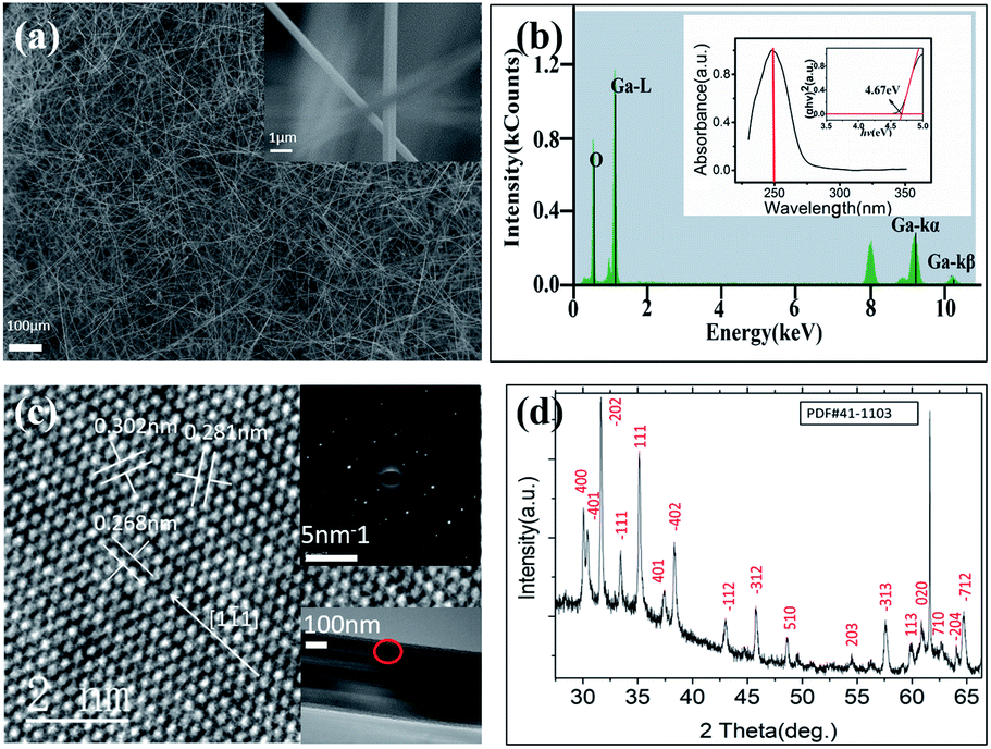
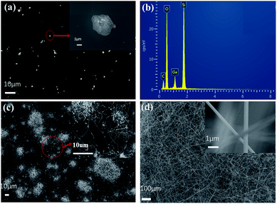
Fig. 1 is the characterization of β-Ga2O3 nanowire networks. Fig. 1a presents SEM photographs of β-Ga2O3 nanowire networks prepared for 15 min at 1150 °C, and the inset is an enlarged image which we can observe the diameter of the nanowire is about 500 nm, the detailed statistics are supplemented in Fig. S2.† Fig. 1b is the EDS spectrum of the nanowire. It further affirms O and Ga elements in the β-Ga2O3 nanowires (NWs). The inset plots the absorption spectrum of the β-Ga2O3 NWs, which strong absorption at deep ultraviolet with an absorption peak at the wavelength of 249 nm and an absorption edge located at ≈275 nm. Besides, by extrapolating the curve of (αhν)2–hν (where α represents absorbance, h represents Planck's constant, and ν represents frequency)48 to zero intensity (inset in Fig. 1b), the optical bandgap of the β-Ga2O3 NWs is determined to be ≈4.67 eV, which coincides with the values in previous reports. The TEM image in Fig. 1c indicates that the nanowire is polycrystalline with lattice spaces of 0.32 and 0.28 nm, which are corresponding to the (400) and (![[1 with combining macron]](https://www.rsc.org/images/entities/char_0031_0304.gif) 11) plane of β-Ga2O3, respectively. Fig. 1d shows XRD patterns of the sample, and all the diffraction peaks can be readily indexed within the monoclinic crystalline phase of β-Ga2O3. The lattice constants were determined to be a = 1.223 nm, b = 3.039 nm, c = 0.581 nm, and β = 103.8°, which is in good agreement with the standard values β-Ga2O3 (JCPDS card no. 41-1103).49 According to the TGA data in Fig. S3,† it can be seen that there is basically no organic matter in the nanowire networks. The above results confirm that β-Ga2O3 NWs with high-crystalline quality have been successfully synthesized.
11) plane of β-Ga2O3, respectively. Fig. 1d shows XRD patterns of the sample, and all the diffraction peaks can be readily indexed within the monoclinic crystalline phase of β-Ga2O3. The lattice constants were determined to be a = 1.223 nm, b = 3.039 nm, c = 0.581 nm, and β = 103.8°, which is in good agreement with the standard values β-Ga2O3 (JCPDS card no. 41-1103).49 According to the TGA data in Fig. S3,† it can be seen that there is basically no organic matter in the nanowire networks. The above results confirm that β-Ga2O3 NWs with high-crystalline quality have been successfully synthesized.
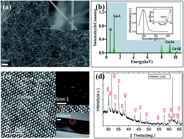 |
| | Fig. 1 SEM/XRD/TEM characterization results for the as-synthesized Ga2O3 NWs on the SiO2/Si substrate (a) high magnification SEM image of β-Ga2O3 sample grown at 1150 °C, inset is a magnification of nanowire network; (b) the EDS spectrum of the nanowire, inset is the absorption spectrum of the β-Ga2O3 nanowire, inset is the plot of (αhv)2 versus hv that gives the bandgap of β-Ga2O3 nanowire; (c) high-resolution TEM image of the single β-Ga2O3 nanowire, inset is SAED image; (d) XRD patterns of the single β-Ga2O3 nanowire. | |
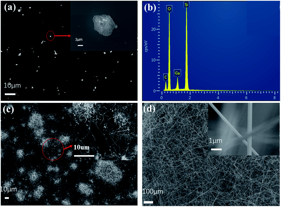
Fig. 2 presents SEM photographs of β-Ga2O3 nanowire networks prepared of 1 min, 5 min, and 15 min at 1150 °C, respectively. According our experiments data, the nanowire length growth speed is very fast. The nanowires length is measured after it was synthesized in different growth time, such as, 1 minute, 5 minutes, 10 minutes, 15 minutes, 20 minutes. A 2.0 mm nanowire length was achieved at a 30 minutes growth time. The diameter of the nanowire exceeded 1.0 μm when the reaction time exceeds 20 minutes in Fig. S4.† Usually, this kind of over 1.0 μm diameter nanowires is not belong to nanoscale category. So, the nanowires sample with 15 minutes growth time was selected to fabricate the photodetector devices. At the beginning of the reaction, it can be seen from Fig. 1a that irregular gallium suboxide (Ga2O) particles are deposited on the substrate and the inset is enlarged image of Ga2O particles.50 The particle size is about 200 nm. Fig. 2b shows the EDS spectrum of particles that the Gallium is observed clearly. It indicates the VS growth mechanism for the nanowire. The Ga2O3 is reduced by liquid metallic gallium and forms a gas phase of Ga2O. The Ga2O gas-phase gets transported to cooler regions and decomposes to liquid gallium and Ga2O3, leading to a vapour–solid (VS) growth mechanism. After the reaction for 5 minutes, we could observe some β-Ga2O3 NWs sprout from the nuclei and the β-Ga2O3 NWs have already contacted with the ones from neighbour pillars and even form some multi-channel junctions, but the β-Ga2O3 NWs density is still relatively low with most of the area between substrates uncovered, as indicated in Fig. 2c, the diameter of β-Ga2O3 NW is about 100 nm. After a growth time of 15 minutes, the β-Ga2O3 NWs covered all the substrates, as indicated in Fig. 2d, the diameter of β-Ga2O3 NWs is about 500 nm.49
 |
| | Fig. 2 High magnification SEM image of the β-Ga2O3 sample grown at 1150 °C, the insets magnify nanowire networks. (a) 1 minute, inset is a magnification of particles; (c) 5 minutes; (d) 15 minutes; (b) the EDS spectrum of particle in (a). | |
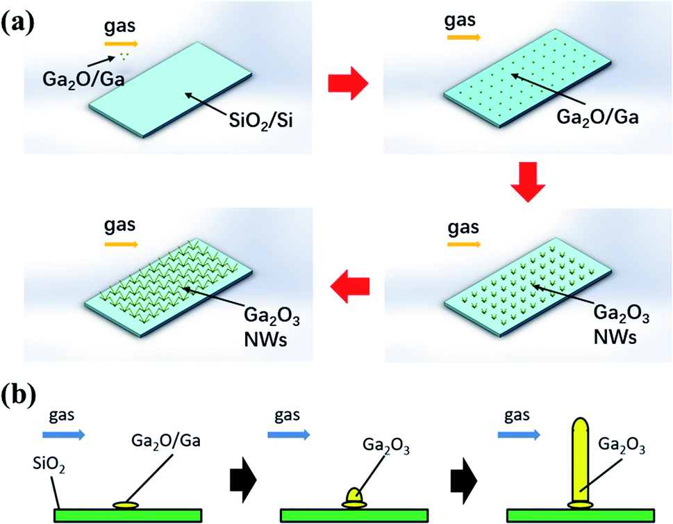
In this paper, the growth process of nanowires is a specific process through a vapor–solid (VS) process; that is, in the absence of any liquid phase, the precursor material is directly deposited on the substrate by gas and becomes a solid under high-temperature heating.51,52 In the present growth mechanism, no additional metallic catalysts are involved, and a liquid Ga droplet is believed to be a self-catalyst for the growth of β-Ga2O3 ribbons. So, we termed the process a self-catalyst growth. The schematic diagram of the nanowire network's growth mechanism is shown in Fig. 3a. After the precursor material (Ga2O3 powder) is heated to the target temperature, Ga or Ga2O vapor will be generated. Next, the generated Ga and Ga2O vapor rush along with the gas flow and then reached the substrate by the gas carrier. Then, Ga and Ga2O react synchronously with the rest of oxygen to form condensed clusters, then crystallize and nucleate. As the temperature increases, the vapor pressure continues to increase with the temperature. A VS mechanism will drive highly anisotropic β-Ga2O3 NWs growth. When the supersaturated vapor pressure in the tube increases to higher than the equilibrium vapor pressure of the cylindrical sidewall of NWs, growth will begin. Finally, due to lattice mismatch, several one-dimensional β-Ga2O3 nanowires are formed. As time goes by, the nanowires stretch and widen and connect to form a network. Eqn (1)–(4) describe the specific reaction process:53
| | |
Ga2O3(S) + 2C(S) → Ga2O(V) + 2CO(g)
| (1) |
| | |
Ga2O3(S) + 3C(S) → 2Ga(V) + 3CO(g)
| (2) |
| | |
Ga2O(V) + 2O2(S) → Ga2O3(S)
| (3) |
| | |
4Ga(S) + 3O2(S) → 2Ga2O3(S)
| (4) |
 |
| | Fig. 3 The schematic diagram of the (a) β-Ga2O3 nanowire networks; (b) single β-Ga2O3 nanowire. | |
Fig. 3b shows a schematic diagram of the nanowires self-catalyst grown via VS process at high temperature, where Ga/Ga2O nanoparticles deposited on the top of the substrate and induce the further growth of nanowires. At higher temperatures, the high vapor pressure of Ga/Ga2O could induce supersaturation around the catalyst droplet (Ga/Ga2O droplet) quickly, resulting in the formation of a large-size catalyst droplet, which is the reason for self-catalyst growth.51 In these grown Ga2O3 nanowires, surface diffusion transport and direct nucleation of species from the vapor phase dominate nanowire growth. Faster surface diffusion transport and direct nucleation of species from the vapor phase could significantly enhance the growth of nanowires. In this growth method that used nano-diamond as carbon sources, more Ga/Ga2O could be reduced simultaneously. Therefore, it is the reason why this method can grow longer and thicker nanowire networks in a short time.
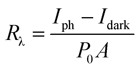
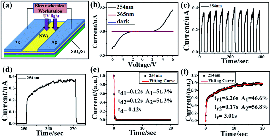
To check its photoelectrical performance, β-Ga2O3 nanowires network directly grown on SiO2/Si substrate in 15 minutes is fabricated for the photoelectrical device. A typical metal–semiconductor–metal structure photodetector with internal space around 2 mm between two Ag electrodes is shown Fig. 4a, with Ag metal electrodes are made on the nanowires network by using silver paste paint in Fig. S6.† A measurement of spectral response of the photodetector from 245 nm to 600 nm wavelength was performed. The device has remarkable spectral response in the band less than 280 nm wavelength, especially around 265 nm wavelength, but almost no response in the wavelength which is larger than 400 nm. The deep ultraviolet (DUV)/visible rejection ratio R250/R400 is about 1.45 × 10³ at 10 V bias is shown in the Fig. S5.† Fig. 4b illustrates the I–V characteristics of the photodetector in the dark, under light illumination of 254 nm and 365 nm with a bias of ±6 V. It is evident that the current under 254 nm illumination is much higher than that of non-illumination and 365 nm, which means the 254 nm illumination could significantly enhance the conductivity of the nanowires network device. Besides, the β-Ga2O3 NWs network photodetector was non-sensitive to 365 nm illumination. The dark current is around 4.17 × 10⁻¹¹ A, and the light current is around 4.45 × 10⁻⁷ A, and the on–off ratios (I254nm/Idark) are about 103. The I–V diagram showed an asymmetric curve because of the formation of Schottky contacts between β-Ga2O3 NWs and Ag. Fig. 4c and d show I–T characteristics of photodetector under 6 V bias. The responsivity (Rλ) is defined as the ratio of the response current to the illumination power on photodetector as given by:11
| |
 | (5) |
where
Iph is the photocurrent,
Idark is the dark current,
P0 is the optical power density, and
A is the effective illumination area. The responsivity of β-Ga
2O
3 is 0.38 A W
−1. The external quantum efficiency (EQE)
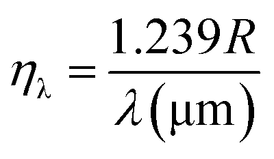
ηλ is defend as the number of charge carriers generated per number of incident photons on the device as given by:
54| |
 | (6) |
where
λ is the wavelength of the incident light. Associated with the above equation,
ηλ = 185.4% could be obtained.
Fig. 4e and f displays the photoresponse of β-Ga
2O
3 NW networks photodetector. The dependence of both rising and decay of photocurrent on time can be investigated by using the second-order decay function as follows:
| | |
y0 = A1et/t1 + A2et/t2
| (7) |
where
t1 and
t2 are time constants of fast and slow processes,
A1 and
A2 are their relative weight factors, respectively,
y0 also is a constant.
tr1 and
tr2 are the time constants of fast and slow current in the rising process;
td1 and
td2 are the time constants of fast and slow current in the decay process. Under the effect of 254 nm light, the rise time
tr and decay time
td is 3.01 s and 0.12 s, respectively.
 |
| | Fig. 4 The device schematic and the photo response characterization (a) the schematic diagram of the β-Ga2O3 UV photodetector; (b) I–V characteristics of β-Ga2O3 nanowires network photodetector in a dark condition, under 365 nm and 254 nm light irradiation, respectively; (c) I–T characteristics of β-Ga2O3 nanowires network photodetector under 6 V bias with 254 nm light irradiation; (d–f) relationship between the rise/decay time and normalized current of β-Ga2O3 nanowires network photodetector. | |
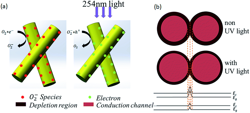
It is well agreed that the chemisorption/desorption of oxygen molecules rules photo response processes in the β-Ga2O3 NWs network. Fig. 5a reveals the adsorption/desorption of oxygen molecules during the DUV response and recovery processes in the β-Ga2O3 NWs. Eqn (10)–(12) describe the specific reaction process:55
| | |
O2(g) + e− → O2−(ad)
| (10) |
| | |
h+ + O2−(ad) → O2(g)
| (12) |
 |
| | Fig. 5 (a) Schematic of carrier generation; (b) NW–NW junction barrier for electron transfer in the NW network device. | |
The oxygen gas molecules adsorbed on the surface of β-Ga2O3 NW to form O2− by capturing free electrons from β-Ga2O3 NW surface (eqn (10)), creating a highly resistive depletion layer near theβ-Ga2O3 NW surface; Under UV illumination, electron–hole pairs are generated (eqn (11)), the holes transport to the β-Ga2O3 NW surface and neutralize the O2−, desorbing the oxygen from the β-Ga2O3 NW surface (eqn (12)). This hole-capturing process increases the free-carrier concentration, producing an apparent enhancement in conductivity. When the UV irradiation is switched off, holes recombine with electrons, and oxygen molecules are re adsorbed on the β-Ga2O3 NW surface by capturing electrons, which increases the resistance of the β-Ga2O3 NW again. The resistance of two crossed NWs is dominated by the NW–NW junction barrier instead of the resistance of the NWs themselves. In our β-Ga2O3 NW network photodetectors, the electrons must overcome the NW–NW junction barrier during the transfer process.53 As discussed above the Fig. 5b, the depletion layer can be narrowed by UV illumination due to an increase in carrier density, which is equivalent to a decrease in low barrier height, to pass through the NW network easily upon UV illumination.
Conclusions
In conclusion, the self-catalyst β-Ga2O3 nanowire networks on an insulating substrate were synthesized rapidly via a catalyst-free and straightforward CVD method. The wide bandgap of the NWs indicates their potential use as efficient UV photodetectors, and their large bandgap of 4.67 eV makes them potential candidates for deep UV detection applications requiring high wavelength selectivity. Simultaneously, the shape changes of the β-Ga2O3 nanowires during the growth process were explored. The diameter of the nanowires can grow from 100 nm to 1 μm. The principle and process of autocatalytic growth are briefly explained. The NWs network devices developed in this work showed a ratio (103) of light current to dark current, and response and recovery times (within 3.01 s and 0.12 s, respectively), and the external quantum efficiency (EQE) is about 185.4% under 254 nm DUV light illumination, which could be attributed to their NW–NW junction barrier-dominant conductance. This value of on–off ratio is not lower than that of β-Ga2O3 photodetector reported by other researchers. The procedures described in this work can be readily extended to other metal oxide nanomaterials for fabricating large area nanoscale electronics through the bottom up process by reducing electrical artefact and reducing the cost of production.
Conflicts of interest
There are no conflicts to declare.
Acknowledgements
Sample synthesis, regular sample characterization, and electrochemical performance tests were carried out at the Chongqing Institute of Green and Intelligent Technology (CIGIT). TEM images were obtained in the Analytical and Testing Center of Chongqing University. All authors acknowledge the support from the Dean Project of Guangxi Key Laboratory of Wireless Wideband Communication and Signal Processing (Grant No. GXKL06190104, GXKL06190105), the National Natural Science Foundation of China (Grant No. 12064005), Western Light Program of the Chinese Academy of Sciences, the Youth Innovation Promotion Association of the Chinese Academy of Sciences under Award No. 2019374.
Notes and references
- H. Chen, K. Liu, L. Hu, A. A. Al-Ghamdi and X. Fang, Mater. Today, 2015, 18, 493–502 CrossRef CAS.
- L. Sang, M. Liao and M. Sumiya, Sensors, 2013, 13, 10482–10518 CrossRef CAS PubMed.
- E. Monroy, F. Omnes and F. Calle, Semicond. Sci. Technol., 2003, 18, R33–R51 CrossRef CAS.
- Y. A. Zou, Y. Zhang, Y. M. Hu and H. S. Gu, Sensors, 2018, 18, 2072 CrossRef PubMed.
- T. Oshima, T. Okuno, N. Arai, N. Suzuki, H. Hino and S. Fujita, Jpn. J. Appl. Phys., 2009, 48, 011605 CrossRef.
- Z. Y. Xu and B. M. Sadler, IEEE Commun. Mag., 2008, 46, 67–73 Search PubMed.
- G. Chen, Z. Xu, H. Ding and B. M. Sadler, Opt. Express, 2009, 17, 3929–3940 CrossRef CAS PubMed.
- M. Razeghi and A. Rogalski, J. Appl. Phys., 1996, 79, 7433–7473 CrossRef CAS.
- H. W. Song, L. X. Yu, S. Z. Lu, T. Wang, Z. X. Liu and L. M. Yang, Appl. Phys. Lett., 2004, 85, 470–472 CrossRef CAS.
- X. Han, S. L. Feng, Y. M. Zhao, L. Li, Z. Y. Zhan, Z. Y. Tao, Y. X. Fan, W. Q. Lu, W. B. Zuo and D. J. Fu, RSC Adv., 2019, 9, 1394–1402 RSC.
- Y. M. Zhao, S. L. Feng, H. T. Jiang, S. Ma, Z. Y. Tao, W. Q. Lu and Y. X. Fan, Phys. E, 2019, 107, 1–4 CrossRef CAS.
- H. T. Jiang, L. Li, S. L. Feng and W. Q. Lu, Phys. E, 2018, 104, 314–319 CrossRef CAS.
- H. T. Jiang, S. B. Liu, L. Y. Liang and W. Q. Lu, RSC Adv., 2018, 8, 28928–28933 RSC.
- Z. Y. Zhan, L. P. Xu, J. N. An, H. J. Du, Z. K. Weng and W. Q. Lu, Adv. Eng. Mater., 2017, 19, 1700101 CrossRef.
- H. H. Tippins, Phys. Rev., 1965, 140, A316–A319 CrossRef.
- G. C. Hu, C. X. Shan, N. Zhang, M. M. Jiang, S. P. Wang and D. Z. Shen, Opt. Express, 2015, 23, 13554–13561 CrossRef CAS PubMed.
- Z. P. Wu, G. X. Bai, Y. Y. Qu, D. Y. Guo, L. H. Li, P. G. Li, J. H. Hao and W. H. Tang, Appl. Phys. Lett., 2016, 108, 4166–4168 Search PubMed.
- W. Y. Kong, G. A. Wu, K. Y. Wang, T. F. Zhang, Y. F. Zou, D. D. Wang and L. B. Luo, Adv. Mater., 2016, 28, 10725–10731 CrossRef CAS PubMed.
- W. Feng, X. Wang, J. Zhang, L. Wang, W. Zheng, P. Hu, W. Cao and B. Yang, J. Mater. Chem. C, 2014, 2, 3254–3259 RSC.
- X. Chen, K. Liu, Z. Zhang, C. Wang, B. Li, H. Zhao, D. Zhao and D. Shen, ACS Appl. Mater. Interfaces, 2016, 8, 4185–4191 CrossRef CAS PubMed.
- L.-H. Zeng, M.-Z. Wang, H. Hu, B. Nie, Y.-Q. Yu, C.-Y. Wu, L. Wang, J.-G. Hu, C. Xie, F.-X. Liang and L.-B. Luo, ACS Appl. Mater. Interfaces, 2013, 5, 9362–9366 CrossRef CAS PubMed.
- S. Oh, C.-K. Kim and J. Kim, ACS Photonics, 2018, 5, 1123–1128 CrossRef CAS.
- W. Y. Weng, T. J. Hsueh, S.-J. Chang, G. J. Huang and S. C. Hung, IEEE Trans. Nanotechnol., 2011, 10, 1047–1052 Search PubMed.
- L. Binet and D. Gourier, J. Phys. Chem. Solids, 1998, 59, 1241–1249 CrossRef CAS.
- S. Geller, J. Chem. Phys., 1960, 33, 676–684 CrossRef CAS.
- M. Orita, H. Ohta, M. Hirano and H. Hosono, Appl. Phys. Lett., 2000, 77, 4166–4168 CrossRef CAS.
- R. Roy, V. G. Hill and E. F. Osborn, J. Am. Chem. Soc., 1952, 74, 719–722 CrossRef CAS.
- X. M. Sun and Y. D. Li, Angew. Chem., Int. Ed., 2004, 43, 3827–3831 CrossRef CAS PubMed.
- N. Ueda, H. Hosono, R. Waseda and H. Kawazoe, Appl. Phys. Lett., 1997, 70, 3561–3563 CrossRef CAS.
- X. Wang, Q. Xu, M. Li, S. Shen, X. Wang, Y. Wang, Z. Feng, J. Shi, H. Han and C. Li, Angew. Chem., Int. Ed., 2012, 51, 13089–13092 CrossRef CAS PubMed.
- M. Higashiwaki, K. Sasaki, A. Kuramata, T. Masui and S. Yamakoshi, Appl. Phys. Lett., 2012, 100, 013504 CrossRef.
- S. J. Pearton, J. Yang, P. H. Cary, F. Ren, J. Kim, M. J. Tadjer and M. A. Mastro, Appl. Phys. Rev., 2018, 5, 011301 Search PubMed.
- Y. Li, T. Tokizono, M. Liao, M. Zhong, Y. Koide, I. Yamada and J.-J. Delaunay, Adv. Funct. Mater., 2010, 20, 3972–3978 CrossRef CAS.
- L. Li, E. Auer, M. Liao, X. Fang, T. Zhai, U. K. Gautam, A. Lugstein, Y. Koide, Y. Bando and D. Golberg, Nanoscale, 2011, 3, 1120–1126 RSC.
- R. Zou, Z. Zhang, Q. Liu, J. Hu, L. Sang, M. Liao and W. Zhang, Small, 2014, 10, 1848–1856 CrossRef CAS PubMed.
- W. Y. Weng, T. J. Hsueh, S. J. Chang, G. J. Huang and S. P. Chang, IEEE Photonics Technol. Lett., 2010, 22, 709–711 CAS.
- P. Feng, J. Y. Zhang, Q. H. Li and T. H. Wang, Appl. Phys. Lett., 2006, 88, 153107 CrossRef.
- C. Xie and F. Yan, Small, 2017, 13, 1701822 CrossRef PubMed.
- T. He, Y. Zhao, X. Zhang, W. Lin, K. Fu, C. Sun, F. Shi, X. Ding, G. Yu, K. Zhang, S. Lu, X. Zhang and B. Zhang, Nanophotonics, 2018, 7, 1557–1562 CAS.
- L. Zhang, X. Xiu, Y. Li, Y. Zhu, X. Hua, Z. Xie, T. Tao, B. Liu, P. Chen, R. Zhang and Y. Zheng, Nanophotonics, 2020, 9, 4497–4503 CrossRef CAS.
- X. Cao, Y. Xing, J. Li, X. Zhang, T. He, L. Zhang, Y. Ma, K. Xu, J. Zhao, W. Tang and B. Zhang, J. Phys. D: Appl. Phys., 2020, 53, 305103 CrossRef CAS.
- M. Kumar, S. Kumar, N. Chauhan, D. S. Kumar, V. Kumar and R. Singh, Semicond. Sci. Technol., 2017, 32, 085012 CrossRef.
- J.-S. Li, X.-D. Zhang, X. Cao, K. Xu, L. Zhang, Y.-M. Fan and B.-S. Zhang, Nanotechnology, 2020, 31, 02LT01 CrossRef CAS PubMed.
- W. Q. Lu, C. M. Jiang, D. Caudle, C. L. Tang, Q. Sun, J. J. Xu and J. H. Song, Phys. Chem. Chem. Phys., 2013, 15, 13532–13537 RSC.
- J. Singh, S. S. Patil, M. A. More, D. S. Joag, R. S. Tiwari and O. N. Srivastava, Appl. Surf. Sci., 2010, 256, 6157–6163 CrossRef CAS.
- H.-D. Li, H. Lu, D.-D. Sang, D.-M. Li, B. Li, X.-Y. Lue and G.-T. Zou, Chin. Phys. Lett., 2008, 25, 3794–3797 CrossRef CAS.
- P. P. He, S. L. Feng, S. Y. Liu, Q. K. Li, J. W. Qi, Z. Y. Zhan, X. Li, Z. H. Li, J. Shen and W. Q. Lu, RSC Adv., 2015, 5, 105288–105291 RSC.
- S. L. Guo, S. Kang, S. L. Feng and W. Q. Lu, J. Phys. Chem. C, 2020, 124, 4764–4771 CrossRef CAS.
- I. D. Hosein, M. Hegde, P. D. Jones, V. Chirmanov and P. V. Radovanovic, J. Cryst. Growth, 2014, 396, 24–32 CrossRef CAS.
- B. Alhalaili, R. J. Bunk, H. Mao, H. Cansizoglu, R. Vidu, J. Woodall and M. S. Islam, Sci. Rep., 2020, 10, 21434 CrossRef CAS PubMed.
- M. Kumar, V. Kumar and R. Singh, Nanoscale Res. Lett., 2017, 12, 184 CrossRef PubMed.
- L. W. Sun, M. L. Zhao, F. Wang, W. Jiang, J. Y. Guo, J. T. Li and J. Dai, J. Nanosci. Nanotechnol., 2020, 20, 2395–2401 CrossRef CAS PubMed.
- X. C. Wu, W. H. Song, W. D. Huang, M. H. Pu, B. Zhao, Y. P. Sun and J. J. Du, Chem. Phys. Lett., 2000, 328, 5–9 CrossRef CAS.
- L. Li, H. T. Jiang, X. Han, Z. Y. Zhan, H. J. Du, W. Q. Lu, Z. J. Li, Z. Y. Tao and Y. X. Fan, Ceram. Int., 2017, 43, 15978–15985 CrossRef CAS.
- S. Ma, S. L. Feng, S. Kang, F. Wang, X. Fu and W. Q. Lu, Electron. Mater. Lett., 2019, 15, 303–313 CrossRef CAS.
Footnote |
| † Electronic supplementary information (ESI) available. See DOI: 10.1039/d1ra04663b |
|
| This journal is © The Royal Society of Chemistry 2021 |
Click here to see how this site uses Cookies. View our privacy policy here. 
 Open Access Article
 This Open Access Article is licensed under a Creative Commons Attribution-Non Commercial 3.0 Unported Licence
 ab,
Shuanglong Feng
ab,
Shuanglong Feng