
 Open Access Article
 This Open Access Article is licensed under a
 Creative Commons Attribution 3.0 Unported Licence
Electronic properties of a two-dimensional van der Waals MoGe2N4/MoSi2N4 heterobilayer: effect of the insertion of a graphene layer and interlayer coupling
D. K. Pham *
*
Institute of Applied Technology, Thu Dau Mot University, Binh Duong Province, Vietnam. E-mail: phamdinhkhang@tdmu.edu.vn
First published on 25th August 2021
Abstract
van der Waals heterostructures (vdWHs) based on 2D layered materials with select properties are paving the way to integration at the atomic scale, and may give rise to new heterostructures exhibiting absolutely novel physics and versatility. Herein, we investigate the structural and contact types in a 2D vdW heterobilayer between MoGe2N4 and MoSi2N4 monolayers, and the monolayers in the presence of electrical graphene (GR) contact. In the ground state, the MoGe2N4/MoSi2N4 heterobilayer forms type-II band alignment, which effectively promotes the separation of electrons and holes and provides opportunity for further electrons and holes. Thus, the MoGe2N4/MoSi2N4 heterobilayer is promising for designing optoelectronic devices with significantly suppressed carrier-recombination. Interestingly, the insertion of the GR contact to a MoGe2N4/MoSi2N4 heterobilayer gives rise to the formation of a metal/semiconductor contact. Depending on the GR position relative to the MoGe2N4/MoSi2N4 heterobilayer, the GR-based heterostructure can form either an n-type or p-type Schottky contact. Intriguingly, the contact barriers in the GR contacted MoGe2N4/MoSi2N4 heterobilayer are significantly smaller than those in the GR contacted with MoGe2N4 or MoSi2N4 monolayers, suggesting that the GR/MoGe2N4/MoSi2N4 heterostructure offers an effective pathway to reduce the Schottky barrier, which is highly beneficial for improving the charge injection efficiency of the contact heterostructures. More interestingly, by controlling the interlayer coupling through stacking, both the Schottky barriers and contact types in the GR/MoGe2N4/MoSi2N4 heterostructure can be manipulated. Our findings could provide theoretical insight into the design of nanodevices based on a GR and MoGe2N4/MoSi2N4 heterobilayer.
1. Introduction
Two-dimensional (2D) materials1–3 have received extensive interest owing to their intriguing physical and chemical properties and broad device application potential, including in electronics,3,4 nanophotonics,5 optoelectronics6,7 and spintronics.8,9 A plethora of 2D materials, including graphene (GR),10 phosphorene,11,12 transition metal dichalcogenides (TMDCs),13,14 and graphitic carbon nitrides,15–17 have been synthesized experimentally and predicted theoretically. These 2D materials exhibit outstanding properties and unique advantages over conventional bulk materials, and are particularly promising candidates for designing high-performance nanodevices, such as field-effect transistors18 and photodetectors.19Very recently, Hong et al.20 discovered a new family of 2D materials, namely MoSi2N4 monolayers, using chemical vapor deposition (CVD). The MoSi2N4 monolayer is a layered structure, which can be viewed as a MoN2 layer sandwiched between two Si–N bilayers. The MoSi2N4 monolayer exhibits semiconducting characteristics with a band gap of about 1.94 eV, and possesses high carrier mobility up to 1200 cm2 V−1 s−1. This monolayer is also stable and mechanically stronger than most other 2D semiconductors such as MoS2 monolayers. The successful synthesis of MoSi2N4 monolayers has led to a new class of 2D materials with formula MA2Z4,20 where M represents an early transition metal (Mo, W, Cr), A = Si or Ge, and Z = N, P, or As. Motivated by this finding, many theoretical investigations have been performed to explore the electronic, optical and transport properties of MA2Z4 monolayers. For instance, Guo et al.21 studied the electronic properties and transport coefficient of MoSi2N4 monolayers alongside the strain effect, and showed that band gap and Seebeck coefficient of such a monolayer are strain-tunable. Wu and colleagues22 also predicted that the band gap of MSi2N4 (M = Mo, W) monolayers can be altered by strain and electric field, which result in the transformation from indirect to direct band gap semiconductors. Furthermore, MoSi2N4, WSi2N4 and VSi2N4 monolayers are also predicted to be a potential valleytronic materials.23,24 These ever expanding first-principle calculations of MA2Z4 have continually revealed the enormous potential of MA2Z4 monolayers for future high-performance device applications.
Currently, constructing 2D van der Waals (vdW) heterostructures between two or more 2D materials is known to be an effective strategy to explore more new properties and extend the potential applications of the corresponding 2D materials. These 2D vdW heterostructures have been predicted theoretically using first-principles calculations, and synthesized experimentally via several methods, such as CVD and mechanical exfoliation. In addition, 2D vdW heterostructures have new desirable properties which could be used for fabricating high-efficiency nanodevices experimentally, such as for solar cells, field-effect transistors (FFTs), and photodetectors. Recently, the combination between the layers of several MA2Z4 monolayers to form MA2Z4 bilayers,22,25 and between the GR layer and MA2Z4 monolayers,26,27 has received much attention from the scientific community. For instance, Zhong et al.25 investigated the electronic features of MA2Z4 (M = Ti, Cr, Mo; A = Si and Z = N, P) bilayers under the strain effect. They predicted that the electronic properties of the MA2Z4 family are tunable with strain-induced transitions from semiconductor to metal. This finding makes the MA2Z4 family a potential candidate for fabricating electro-mechanical devices. Similarly, Wu and colleagues22 showed that applying an electric field can also tune the semiconductor-to-metal transition in both MoSi2N4 and WSi2N4 bilayers, they are therefore suitable for designing next generation nanoelectronics and optoelectronics. Nonetheless, the combination between MoSi2N4 and MoGe2N4 to form a heterobilayer, and between graphene and MoSi2N4/MoGe2N4 heterobilayer to form a GR/MoSi2N4/MoGe2N4 heterostructure, have not yet been explored thoroughly.
In this work, based on first-principles calculations, we investigate the electronic structures of the MoSi2N4/MoGe2N4 heterobilayer and explore its electronic properties and band alignment alongside the presence of the GR layer. Various combinations and stacking configurations of GR/MoSi2N4/MoGe2N4 heterostructures are investigated. Our results reveal that the MoSi2N4/MoGe2N4 heterobilayer exhibits an indirect band gap semiconductor and possesses type-II band alignment at the equilibrium state. With the presence of the GR layer in the MoSi2N4/MoGe2N4 heterobilayer, we see the formation of the Schottky contact with narrow barrier height of about 0.26 eV, which increases the carrier injection efficiency.
2. Computational details
In this work, all the calculations, including geometric optimization, electronic properties and band alignment of the MoSi2N4/MoGe2N4 heterobilayers and the heterostructures between GR and MoSi2N4/MoGe2N4 heterobilayer, were performed from first-principles calculations within density functional theory, which was implemented in Vienna Ab initio Simulation (VASP)28 and Quantum Espresso29,30 packages. The Perdew–Burke–Ernzerhof (PBE) in the framework of the generalized gradient approximation (GGA)31 was used to describe the exchange–correlation energy. The projector augmented wave (PAW)32 pseudopotentials were used to describe the electron-ion interaction. In addition, the DFT-D3 method of Grimme33 was also selected for describing the presence of the weak vdW forces that always occur in layered vdW systems, including heterobilayers and heterostructures. Furthermore, it should be noted that the traditional DFT method always underestimates the band gap values of materials, especially 2D materials, we therefore used the Heyd–Scuseria–Ernzerhof (HSE06) hybrid functional to avoid this issue and obtain an accurate band gap of the considered materials. The Brillouin zone (BZ) was sampled using the Monkhorst-Pack scheme. A 12 × 12 × 1 (6 × 6 × 1) k-point mesh was used for all the calculations within the DFT-PBE (HSE06) method with a cutoff energy of 510 eV. To avoid the interactions between periodical slabs, we set a large vacuum thickness of 25 Å along the z direction. The geometric optimization was fully obtained with the convergence threshold for energy of 10−6 eV and for a force of 10−3 eV Å−1. The spin–orbit coupling (SOC) was also taken into account for the electronic properties of the heterobilayer.3. Results and discussion
3.1. Structural and electronic properties of MoGe2N4/MoSi2N4 heterobilayer
The relaxed atomic structures of the MoGe2N4/MoSi2N4 heterostructure for AA and AB stacking configurations are depicted in Fig. 1. In AA-stacking, both the Ge and N atoms in the MoGe2N4 layer are located directly above the Si and N atoms of the MoSi2N4 layer, as depicted in Fig. 1(a). Whereas, in AB-stacking, the Ge and N atoms in the MoGe2N4 layer are staggered with respect to the Si and N atoms of the MoSi2N4 layer, as depicted in Fig. 1(b). After geometric optimization, the interlayer spacings (D) between the MoGe2N4 and MoSi2N4 layers for the AA and AB stacking configurations are obtained as listed in Table 1. For the AA-stacking, the equilibrium interlayer spacing is 3.33 Å, and it is 3.35 Å for the AB-stacking configuration. For checking the structural stability of such a heterostructure, we further calculate the binding energy as: Eb = EH − ΣEMi, where EH is the total energy of the combined MoGe2N4/MoSi2N4 heterostructure. EMi is the total energy of the constituent MoGe2N4 and MoSi2N4 monolayers. The binding energy of the MoGe2N4/MoSi2N4 heterobilayer for AA and AB stacking configurations is calculated to be −0.11 and −0.16 eV, respectively. The negative binding energy confirms that the heterobilayer is dynamically stable. In addition, the binding energy of the MoGe2N4/MoSi2N4 heterobilayer for the AB stacking configuration is lower than that for the AA stacking configuration, suggesting that the AB stacking configuration can be considered as the most energetically favorable stacking configuration.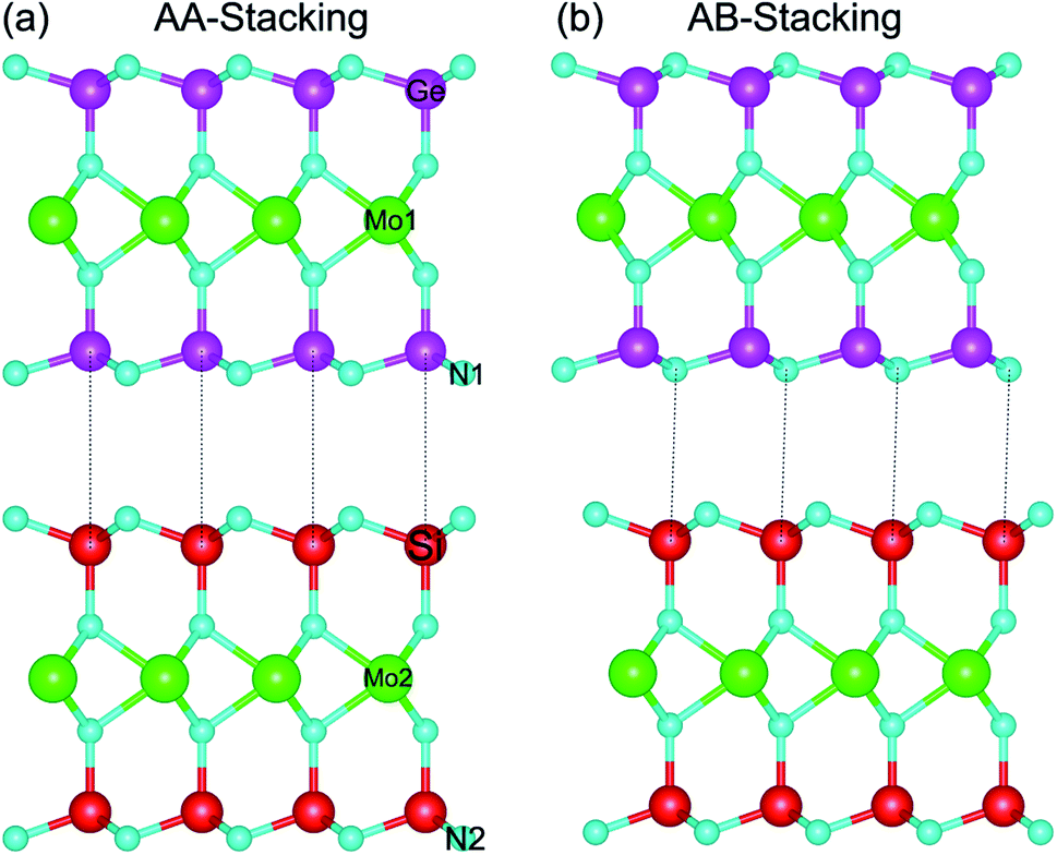 | ||
| Fig. 1 Side view of the optimized atomic structures of the MoGe2N4/MoSi2N4 heterostructure for (a) AA-stacking and (b) AB-stacking. | ||
| a | D | Eb | Eg | Band alignment | |||
|---|---|---|---|---|---|---|---|
| PBE | HSE | PBE + SOC | |||||
| AA-stacking | 2.96 | 3.33 | −0.11 | 0.88 | 1.29 | 0.87 | Type-II |
| AB-stacking | 2.96 | 3.35 | −0.16 | 0.90 | 1.33 | 0.89 | Type-II |
The band structures of the MoGe2N4/MoSi2N4 heterostructure for different stacking configurations are displayed in Fig. 2. We used different methods, including PBE, HSE and PBE + SOC to calculate the band gaps of the considered heterostructure. The obtained band gaps for the MoGe2N4/MoSi2N4 heterostructure are listed in Table 1. For the AA-stacking, the band gaps of the MoGe2N4/MoSi2N4 heterostructure are calculated as 0.88 eV, 1.29 eV and 0.87 eV. It is clear that the HSE06 method gives rise to a larger band gap value than the PBE and PBE + SOC methods. However, all three methods predict the same characters of the MoGe2N4/MoSi2N4 heterostructure, which possesses the indirect band gap semiconductor. The valence band maximum (VBM) is located at the Γ point, while the conduction band minimum (CBM) is located at the M point. Interestingly, when the SOC effect is applied, it tends to split the valence bands at the M point of the MoGe2N4/MoSi2N4 heterostructure into two different parts, as depicted in Fig. 2(c). The energy of band splitting for the first and second valence bands of the AA-stacking is calculated to be 13.27 meV and 13.9 meV, respectively. However, the SOC effect splits only the valence bands at the M point, whereas the VBM of such heterostructure is located at the Γ point. Therefore, the SOC does not affect the band alignments of the heterostructures. Similar trends are also observed in the AB-stacking of the MoGe2N4/MoSi2N4 heterostructure. The PBE, HSE06 and PBE + SOC band gaps of the MoGe2N4/MoSi2N4 heterostructure for the AB-stacking are 0.90, 1.33 and 0.89 eV, respectively. The AB-stacking also predicts the indirect band gap semiconductor in the MoGe2N4/MoSi2N4 heterostructure with the VBM at the Γ point and the CBM at the M point, as depicted in Fig. 2(d–f). Furthermore, the band offset is also critical for the optoelectronic application, we therefore calculate the band offsets for valence bands (ΔV) and for conduction bands (ΔC). The band offsets ΔV and ΔC for the AA-stacking are calculated to be 0.43 eV and 0.47 eV, respectively. Whereas, these values for AB-stacking are 0.40 eV and 0.43 eV, respectively. In addition, comparing AA and AB stacking, the band structure and alignment seems to be almost unchanged. This is a very convenient behaviour for experimental fabrication since the electronic properties are less affected by stacking configurations.
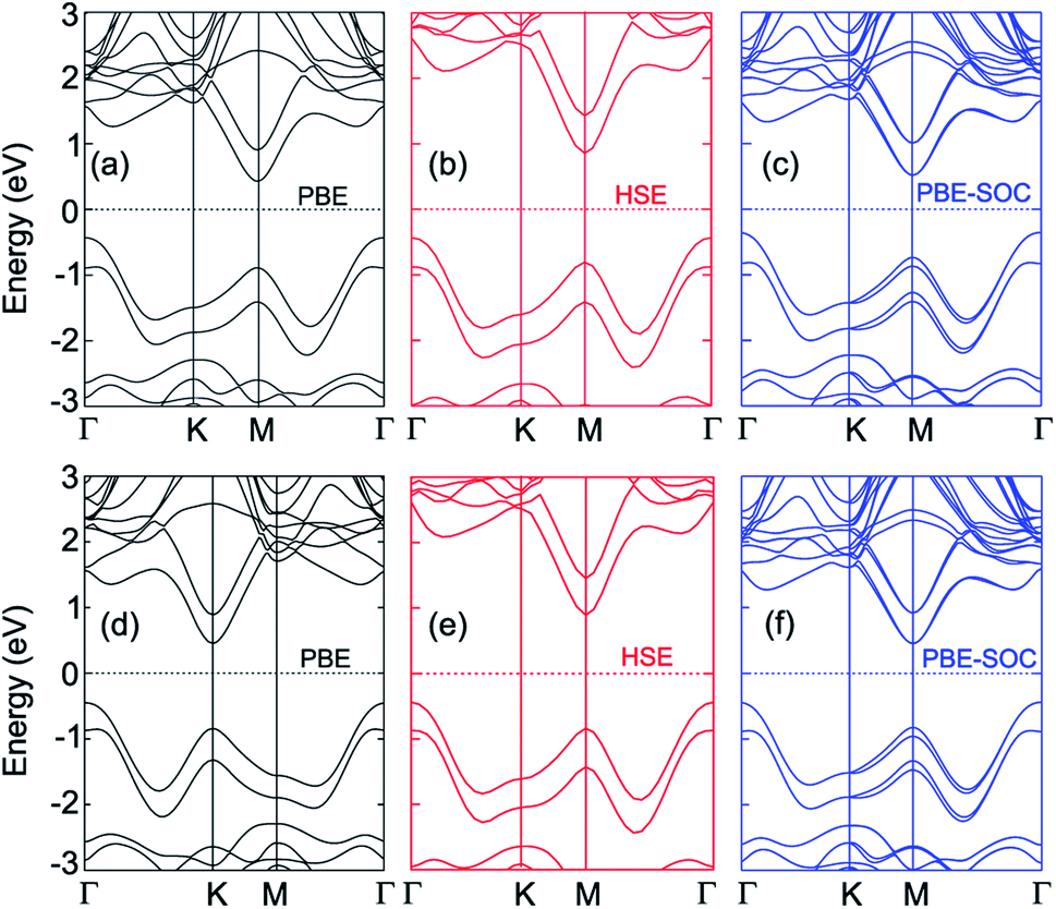 | ||
| Fig. 2 Band structures of the MoGe2N4/MoSi2N4 heterostructure calculated by (a, d) PBE, (b, e) HSE and (c, f) PBE + SOC methods for (a–c) AA-stacking and (d–f) AB-stacking. | ||
More interestingly, device performance based on vdW heterostructures depends crucially on the band alignment, forming between two different 2D materials. Depending on the band edge positions of the constituent monolayers, vdW heterostructure can be divided into three different types of band alignment, including type-I (straddling gap), type-II (staggered gap) and type-III (broken gap). To investigate the band alignment, we further calculate weighted band structures of the MoGe2N4/MoSi2N4 heterostructure, as depicted in Fig. 3. For both the AA-stacking and AB-stacking, one can find that the CBM of the MoGe2N4/MoSi2N4 heterostructure is mainly contributed by the Mo-orbital states of the MoGe2N4 layer, as marked with green circles. Whereas, the VBM at the Γ point is mainly contributed by the Mo-orbital states of the MoSi2N4 layer, as marked by the violet circles. The contributions by the different monolayers to the VBM and CBM demonstrate that the MoGe2N4/MoSi2N4 heterostructure possesses type-II band alignment for both AA- and AB-stacking. The type-II band alignment promotes effective separation of electrons and holes and provides an opportunity for electrons and holes to separate in real space. Thus, the MoGe2N4/MoSi2N4 heterostructure is promising for designing optoelectronic devices with significantly suppressed carrier-recombination.
 | ||
| Fig. 3 Weighted band structures of the MoGe2N4/MoSi2N4 heterostructure for (a) AA-stacking and (b) AB-stacking. | ||
We further investigated the charge mechanism in the MoGe2N4/MoSi2N4 heterobilayer by calculating the charge density difference as follows: Δρ = ρHB − ΣρMi, where ρHB and ρMi, respectively, are the charge density of the MoGe2N4/MoSi2N4 heterobilayer and the constituent MoGe2N4 and MoSi2N4 monolayers. The charge density difference of the MoGe2N4/MoSi2N4 heterobilayer for the AA- and AB stacking is illustrated in Fig. 4. The yellow and cyan regions represent the positive and negative charges, respectively. We find that the charges are mainly visualized at the interface. The yellow regions are located in the MoGe2N4 side, while the cyan regions are in the MoSi2N4 layer. This finding suggests that the charges are mainly accumulated in the MoGe2N4 layer and depleted in the MoSi2N4 layer.
 | ||
| Fig. 4 Charge density difference of the MoGe2N4/MoSi2N4 heterostructure for the (a) AA- and (b) AB-stacking configurations. Yellow and cyan regions represent the positive and negative charges, respectively. The isosurface value is set to be 2.35 e Å−3. | ||
3.2. Electrical graphene contact to a MoGe2N4/MoSi2N4 heterobilayer
We now consider the formation of a triple-layered 2D-metal/2D-semiconductor heterostructure by including a graphene layer into the MoSi2N4/MoGe2N4 heterobilayer. The atomic structures of all vdW heterostructures between the GR and MoSi2N4/MoGe2N4 heterobilayer are depicted in Fig. 5(a–c). Three stacking sequences can be obtained: GR layer placed on top of the MoSi2N4 layer in the MoSi2N4/MoGe2N4 heterobilayer (Fig. 5(a)); GR layer between the MoSi2N4 and MoGe2N4 layers (Fig. 5(b)); and GR layer located below the MoGe2N4 layer in the MoSi2N4/MoGe2N4 heterobilayer (Fig. 5(c)). It is clear that the lattice constant of single-layer GR is calculated to be 2.46 Å, while the lattice constant of the MoSi2N4/MoGe2N4 heterobilayer is calculated to be 2.98 Å. Therefore, in order to avoid the effect of lattice mismatch, we use a supercell, consisting of (2 × 2) unit cells of GR and unit cells of MoSi2N4/MoGe2N4 heterobilayer to build the triple-layered 2D-metal/2D-semiconductors heterostructure. The lattice constant of the triple-layered 2D-metal/2D-semiconductors heterostructure is calculated to be 5.04 Å. Thus, the lattice mismatch between GR and the MoSi2N4/MoGe2N4 heterobilayer is 2.38%, which is reasonably small and does not affect the main results. The interlayer spacings between the GR, MoSi2N4 and MoGe2N4 are calculated and listed in Table 2. For the GR/MoSi2N4/MoGe2N4, the interlayer spacings D1, D2 and D3 are calculated to be 3.58, 13.80 and 3.33 Å, respectively. These values indicate that the interactions between the GR, MoSi2N4 and MoGe2N4 are weak. In addition, we can see that the interlayer spacings of 3.33 Å and 3.58 Å are comparable with those in other 2D-layered heterostructures, which have typical vdW forces.34–37 This finding suggests that the GR, MoSi2N4 and MoGe2N4 layers in their corresponding heterostructures are bonded together via weak vdW interactions. It should be noted that the systems that are characterized by the vdW interactions are feasible and thus they can be easily fabricated in experiments using several common strategies, such as mechanical exfoliation38 and chemical vapor deposition (CVD).39 Furthermore, considering the MoSi2N4/GR/MoGe2N4 and MoSi2N4/MoGe2N4/GR heterostructures, we also find that they are characterized by weak vdW forces. Furthermore, in order to guarantee stability, we also perform the ab initio molecular dynamics simulations of such heterostructures at room temperature of 300 K, as depicted in Fig. 6. We find that the heterostructures are stable at 300 K room temperature.
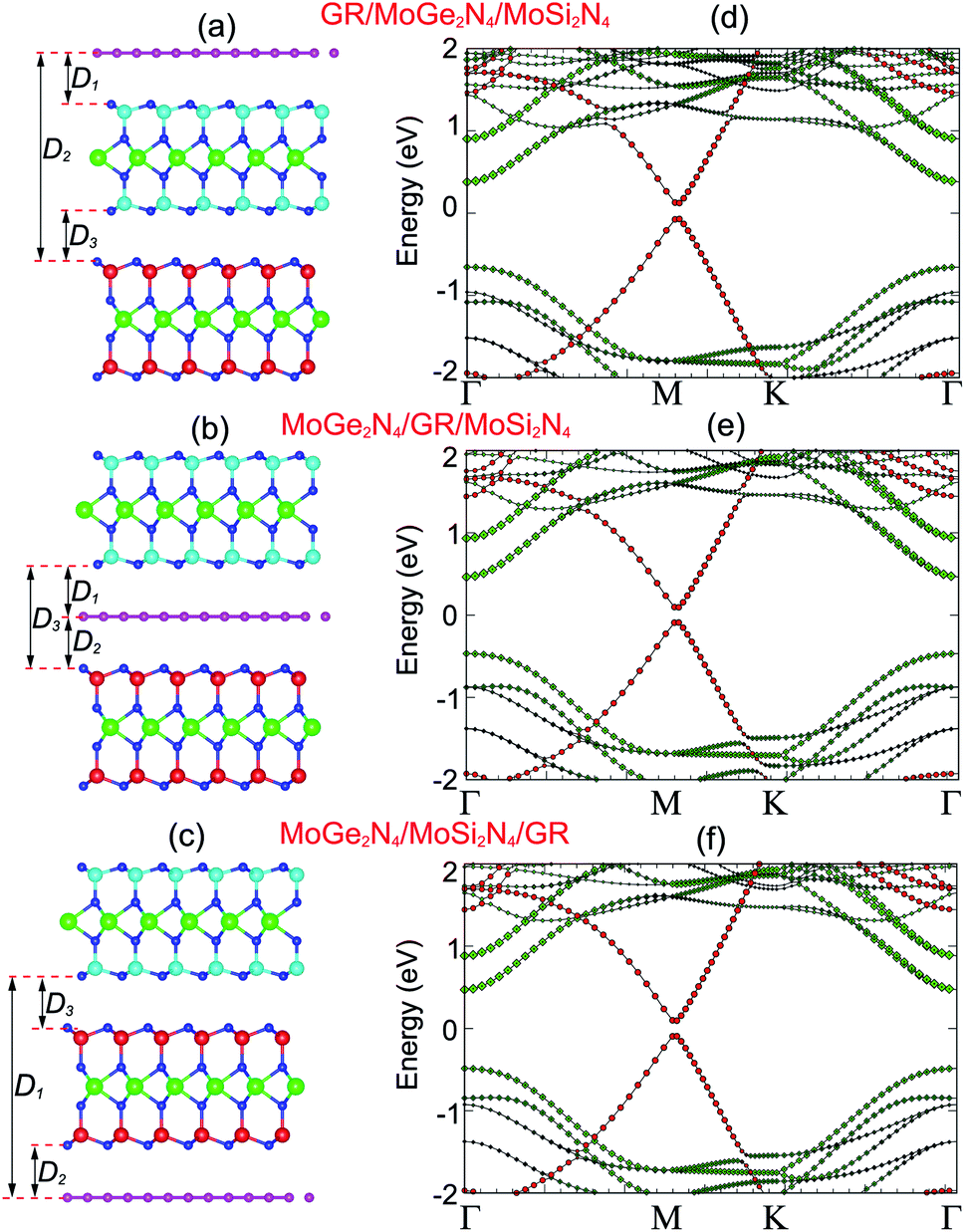 | ||
| Fig. 5 Side view of the atomic structures of (a) GR/MoGe2N4/MoSi2N4, (b) MoGe2N4/GR/MoSi2N4 and (c) MoGe2N4/MoSi2N4/GR heterostructures. Weighted band structures of (d) GR/MoGe2N4/MoSi2N4, (e) MoGe2N4/GR/MoSi2N4 and (f) MoGe2N4/MoSi2N4/GR heterostructures. Red and green circles represent the contributions of semimetal graphene and semiconducting MoGe2N4/MoSi2N4 layers, respectively. | ||
 | ||
| Fig. 6 The variation of the temperature of the considered heterostructures as a function of a time heating step by performing AIMD simulations. The insets represent snapshots of the heterostructures after heating for 4 ps. | ||
| Heterostructures | Interlayer spacings | Eb, meV per C atom | Φn, eV | Φp, eV | EGRg, meV | Contact types | ||
|---|---|---|---|---|---|---|---|---|
| D1, Å | D2, Å | D3, Å | ||||||
| GR/MoSi2N4 (ref. 27) | 3.16 | — | — | −49.14 | 1.49 | 0.96 | 17 | p-type ShC |
| GR/MoGe2N4 (ref. 27) | — | 3.38 | — | −24.86 | 0.63 | 1.54 | 14 | n-type ShC |
| GR/MoSi2N4/MoGe2N4 | 3.58 | 13.80 | 3.33 | −67.66 | 0.33 | 0.61 | 42 | n-type ShC |
| MoSi2N4/GR/MoGe2N4 | 3.70 | 3.67 | 7.37 | −55.73 | 0.43 | 0.41 | 46 | p-type ShC |
| MoSi2N4/MoGe2N4/GR | 14.23 | 3.31 | 3.45 | −65.35 | 0.47 | 0.46 | 45 | p-type ShC |
The projected band structures of the heterostructures combined between the GR and MoSi2N4/MoGe2N4 heterobilayer are depicted in Fig. 5(d–f). Red and green circles represent the contributions of the GR and MoSi2N4/MoGe2N4 layers, respectively. One can observe that the electronic band structures of these graphene-based heterostructures seem to be a combination between those of the constituent GR and MoSi2N4/MoGe2N4 heterobilayer. A Dirac cone with linear dispersion of the GR layer is well preserved and located at the M point. The physical mechanism of the shift in Dirac point from the K to M point is due to the size effects in the GR supercell.40 The semiconducting feature of the MoSi2N4/MoGe2N4 heterobilayer is also maintained. The band gap of the MoSi2N4/MoGe2N4 heterobilayer contacted to the GR layer is about 0.84 eV, which is smaller than that of the freestanding MoSi2N4/MoGe2N4 heterobilayer. This finding suggests that the contact between GR and the MoSi2N4/MoGe2N4 heterobilayer tends to reduce the band gap of the MoSi2N4/MoGe2N4 heterobilayer semiconductor. This reduction gives rise to an enhancement in optical absorption of graphene-based heterostructures. Furthermore, the MoSi2N4/MoGe2N4 heterobilayer contacted with the GR layer possesses a direct band gap semiconductor with both the VBM and CBM at the Γ point, as depicted in Fig. 5(d–f). The nature of such a transformation from an indirect to direct band gap in the MoSi2N4/MoGe2N4 heterobilayer is due to a band folding effect. More interestingly, when GR contacts the MoSi2N4/MoGe2N4 heterobilayer, a band gap of about (17–46) meV is opened in the GR layer. It is clear that the mechanism of this band gap opening in the GR layer is due to symmetry breaking of the A and B sub-lattices in GR. This appearance was also observed in other GR-based heterostructures.35–37
More interestingly, the contact between metallic GR and the semiconducting MoSi2N4/MoGe2N4 heterobilayer gives rise to the formation of a 2D metal/2D semiconductor interface. For the 2D metal/2D semiconductor interface, depending on the position of the Fermi level of metallic GR with respect to the band edges of the semiconductor, there is the formation of either Schottky contact (ShC) or Ohmic contact (OhC). One can find from the band structures in Fig. 5 that the Fermi level of the GR layer lies in the band gap region of the MoSi2N4/MoGe2N4 semiconductor, thus suggesting the formation of the ShC type in all three corresponding GR-based heterostructures. In addition, the Fermi level pinning is still weak in the heterostructures that are characterized by the weak vdW interactions. Therefore, we determine the contact barriers of such heterostructures using the Schottky–Mott rule.41 The n-type and p-type ShC, respectively, can be defined as Φn = EC − EF and Φp = EF − EV, where EC, EV and EF, respectively, are the CBM, VBM and Fermi level of the GR-based heterostructure. The calculated Φn and Φp of the GR/MoGe2N4/MoSi2N4, MoGe2N4/GR/MoSi2N4 and MoGe2N4/MoSi2N4/GR heterostructures are listed in Table 2. We find that the Φn in the GR/MoGe2N4/MoSi2N4 heterostructure is still smaller than the Φp, indicating that it forms an n-type ShC at the equilibrium state. Whereas, for the MoGe2N4/GR/MoSi2N4 and MoGe2N4/MoSi2N4/GR heterostructures, the Φn is higher that the Φp, implying that they form the p-type ShC. The Φn of the MoGe2N4/GR/MoSi2N4 heterostructure is calculated to be 0.33 eV, which is smaller than that of the GR/MoGe2N4/MoSi2N4 and MoGe2N4/MoSi2N4/GR heterostructures, as illustrated in Fig. 7. The lower the contact barrier, the better the device performance. Intriguingly, the contact barriers in the GR contacted MoGe2N4/MoSi2N4 heterobilayer are significantly smaller than those in the GR contacted with MoGe2N4 and MoSi2N4 monolayers, as listed in Table 2. This suggests that the GR/MoGe2N4/MoSi2N4 heterostructure offers an effective pathway to reduce the Schottky barrier, which is highly beneficial for improving the charge injection efficiency of contact heterostructures.
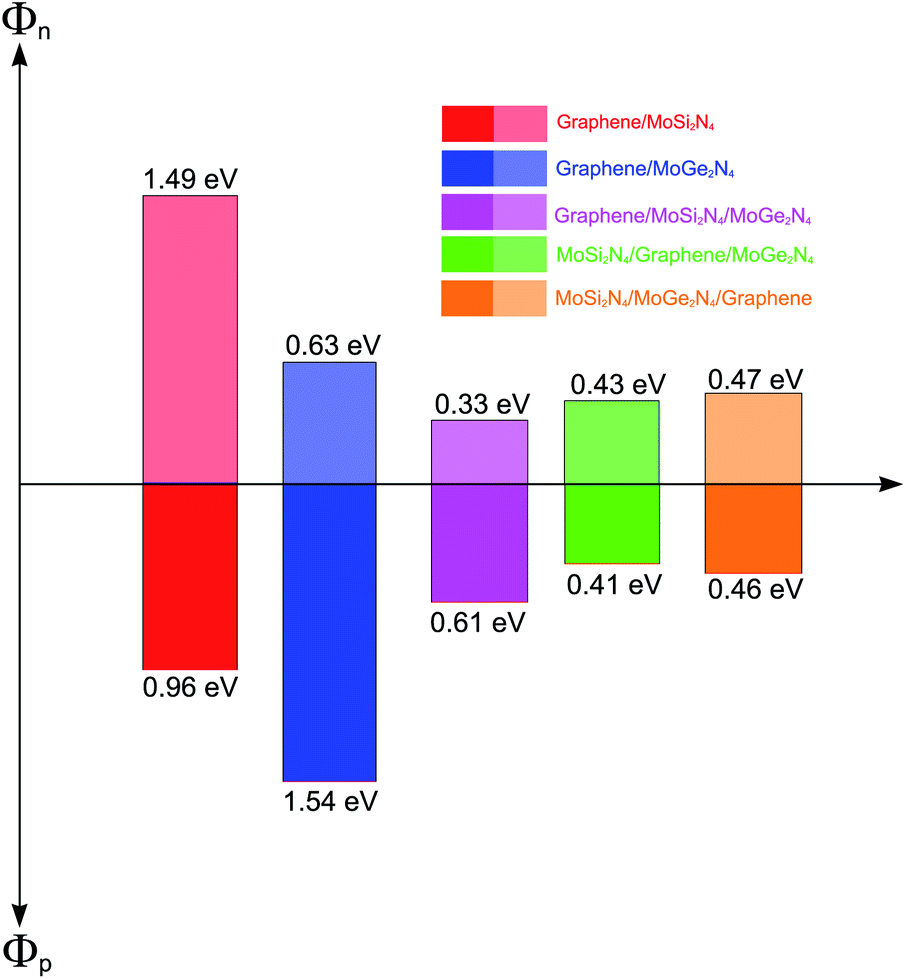 | ||
| Fig. 7 Histogram of the Schottky barrier height of the vdW heterostructures formed between graphene, MoSi2N4 and MoGe2N4 monolayers. | ||
The tuning of the contact barriers and contact types in GR-based vdW heterostructures is an important factor of nanodevices based on the GR heterostructures. Controlling the interlayer coupling through stacking is one of the most efficient strategies in tuning both the contact barriers and contact types of GR-based heterostructures. The interlayer coupling can be manipulated by changing the interlayer spacings between the GR and semiconductors in their corresponding heterostructures. One can observe from Table 2 that the GR/MoGe2N4/MoSi2N4 has the lowest binding energy of −67.66 meV per C atom in comparison with that of other configurations, as it is the most stable configuration. Therefore, the effects of the interlayer couplings on the contact barriers and contact types of the GR/MoGe2N4/MoSi2N4 heterostructure are investigated as an illustrative example. The projected band structures of the GR/MoGe2N4/MoSi2N4 heterostructure as well as the variation in the contact barriers as functions of the interlayer couplings are displayed in Fig. 8. Red and black lines represent the contributions of the metallic GR and semiconducting MoGe2N4/MoSi2N4 heterobilayer, respectively.
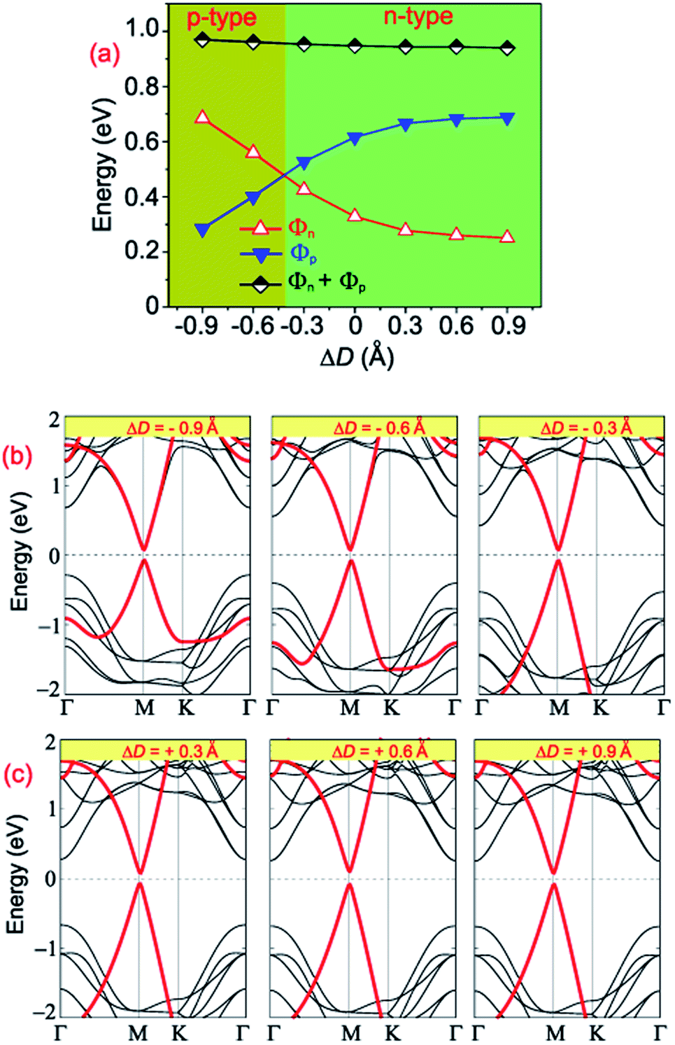 | ||
| Fig. 8 (a) The variation of the Schottky barriers of the GR/MoGe2N4/MoSi2N4 heterostructure as a function of the interlayer couplings. Projected band structures of the GR/MoGe2N4/MoSi2N4 heterostructure under (b) compressive and (c) tensile strains. | ||
Interestingly, we find that changing interlayer couplings gives rise to a change not only in the Schottky barriers but also in the contact types of the GR/MoGe2N4/MoSi2N4 heterostructure. The changes in the Schottky barriers and contact types in the GR/MoGe2N4/MoSi2N4 heterostructure are illustrated in Fig. 8(a). The Φn decreases with increasing interlayer spacing, while the Φp increases accordingly. On the contrary, the Φn increases with decreasing the interlayer spacing, while the Φp decreases accordingly. When the ΔD is smaller than −0.45 Å, the Φn becomes larger than the Φp, leading to the transition from n-type ShC to p-type. The physical mechanism of such transitions can be described by analyzing the change in the Fermi level relative to the band edges of the semiconducting MoGe2N4/MoSi2N4 heterobilayer. With the applications of the compressive strain, i.e. ΔD < 0, the Fermi level of graphene moves towards the VBM of the semiconducting MoGe2N4/MoSi2N4 heterobilayer, thus resulting in an/a increase/decrease in the Φn/Φp. On the other hand, with the application of the tensile strain, i.e. ΔD > 0, the Fermi level of graphene shifts upwards from the VBM to the CBM of the semiconducting MoGe2N4/MoSi2N4 heterobilayer. Thus, the Φn is decreased and the Φp is increased accordingly. In this case, the heterostructure remains as n-type ShC. It can be concluded that with the application of different strains, both the Schottky barriers and contact types in the GR/MoGe2N4/MoSi2N4 heterostructure can be manipulated.
4. Conclusions
In summary, we have investigated the structural and contact types in a 2D vdW heterobilayer between MoGe2N4 and MoSi2N4 monolayers, as well as in the presence of electrical graphene. We found that the MoGe2N4/MoSi2N4 heterobilayer forms type-II band alignment, which effectively promotes the separation of electrons and holes, and provides an opportunity for further electrons and holes. Interestingly, the insertion of the electrical graphene contact to a MoGe2N4/MoSi2N4 heterobilayer gives rise to the formation of a metal/semiconductor contact, which is characterized by the contact type barriers. Depending on the graphene position relative to the MoGe2N4/MoSi2N4 heterobilayer, the graphene-based heterostructure can form either an n-type or p-type Schottky contact. The graphene/MoGe2N4/MoSi2N4 heterostructure exhibits an n-type Schottky contact, whereas the MoGe2N4/GR/MoSi2N4 and MoGe2N4/MoSi2N4/GR heterostructures form a p-type one. Intriguingly, the contact barriers in the GR contacted MoGe2N4/MoSi2N4 heterobilayer are significantly smaller than those in the GR contacted MoGe2N4 and MoSi2N4 monolayers, suggesting that the GR/MoGe2N4/MoSi2N4 heterostructure offers an effective pathway to reduce the Schottky barrier, which is highly beneficial for improving the charge injection efficiency of the contact heterostructures. More interesting, by controlling the interlayer coupling through stacking, both the Schottky barriers and contact types in the GR/MoGe2N4/MoSi2N4 heterostructure can be manipulated.Conflicts of interest
There are no conflicts to declare.Acknowledgements
The author wishes to thank Prof. Yee Sin Ang (Singapore University of Technology and Design, Singapore) for critically reading the manuscript and helpful discussion.References
- S. Z. Butler, S. M. Hollen, L. Cao, Y. Cui, J. A. Gupta, H. R. Gutiérrez, T. F. Heinz, S. S. Hong, J. Huang and A. F. Ismach, et al., ACS Nano, 2013, 7, 2898 CrossRef CAS PubMed.
- P. Miró, M. Audiffred and T. Heine, Chem. Soc. Rev., 2014, 43, 6537 RSC.
- G. Fiori, F. Bonaccorso, G. Iannaccone, T. Palacios, D. Neumaier, A. Seabaugh, S. K. Banerjee and L. Colombo, Nat. Nanotechnol., 2014, 9, 768 CrossRef CAS PubMed.
- X. Li, L. Tao, Z. Chen, H. Fang, X. Li, X. Wang, J.-B. Xu and H. Zhu, Appl. Phys. Rev., 2017, 4, 021306 Search PubMed.
- F. Xia, H. Wang, D. Xiao, M. Dubey and A. Ramasubramaniam, Nat. Photonics, 2014, 8, 899 CrossRef CAS.
- S. Lei, F. Wen, B. Li, Q. Wang, Y. Huang, Y. Gong, Y. He, P. Dong, J. Bellah and A. George, et al., Nano Lett., 2015, 15, 259 CrossRef CAS PubMed.
- J. S. Ponraj, Z.-Q. Xu, S. C. Dhanabalan, H. Mu, Y. Wang, J. Yuan, P. Li, S. Thakur, M. Ashrafi and K. Mccoubrey, et al., Nanotechnology, 2016, 27, 462001 CrossRef PubMed.
- X. Li and X. Wu, Wiley Interdiscip. Rev.: Comput. Mol. Sci., 2016, 6, 441 CAS.
- Y. Liu, C. Zeng, J. Zhong, J. Ding, Z. M. Wang and Z. Liu, Nano-Micro Lett., 2020, 12, 1 CrossRef.
- K. S. Novoselov, A. K. Geim, S. V. Morozov, D. Jiang, Y. Zhang, S. V. Dubonos, I. V. Grigorieva and A. A. Firsov, Science, 2004, 306, 666 CrossRef CAS PubMed.
- Y. Jing, X. Zhang and Z. Zhou, Wiley Interdiscip. Rev.: Comput. Mol. Sci., 2016, 6, 5 CAS.
- A. Carvalho, M. Wang, X. Zhu, A. S. Rodin, H. Su and A. H. C. Neto, Nat. Rev. Mater., 2016, 1, 1 Search PubMed.
- S. Manzeli, D. Ovchinnikov, D. Pasquier, O. V. Yazyev and A. Kis, Nat. Rev. Mater., 2017, 2, 1 Search PubMed.
- W. Choi, N. Choudhary, G. H. Han, J. Park, D. Akinwande and Y. H. Lee, Mater. Today, 2017, 20, 116 CrossRef CAS.
- S. Yang, Y. Gong, J. Zhang, L. Zhan, L. Ma, Z. Fang, R. Vajtai, X. Wang and P. M. Ajayan, Adv. Mater., 2013, 25, 2452 CrossRef CAS.
- Q. Liang, Z. Li, Z.-H. Huang, F. Kang and Q.-H. Yang, Adv. Funct. Mater., 2015, 25, 6885 CrossRef CAS.
- L. Tan, C. Nie, Z. Ao, H. Sun, T. An and S. Wang, J. Mater. Chem. A, 2021, 9, 17 RSC.
- C. Klinkert, Á. Szabó, C. Stieger, D. Campi, N. Marzari and M. Luisier, ACS Nano, 2020, 14, 8605 CrossRef CAS PubMed.
- F. Yan, Z. Wei, X. Wei, Q. Lv, W. Zhu and K. Wang, Small Methods, 2018, 2, 1700349 CrossRef.
- Y.-L. Hong, Z. Liu, L. Wang, T. Zhou, W. Ma, C. Xu, S. Feng, L. Chen, M.-L. Chen and D.-M. Sun, et al., Science, 2020, 369, 670 CrossRef CAS PubMed.
- X.-S. Guo and S.-D. Guo, Chin. Phys. B, 2021, 30, 067102 CrossRef.
- Q. Wu, L. Cao, Y. S. Ang and L. K. Ang, Appl. Phys. Lett., 2021, 118, 113102 CrossRef CAS.
- S. Li, W. Wu, X. Feng, S. Guan, W. Feng, Y. Yao and S. A. Yang, Phys. Rev. B, 2020, 102, 235435 CrossRef CAS.
- Q. Cui, Y. Zhu, J. Liang, P. Cui and H. Yang, Phys. Rev. B, 2021, 103, 085421 CrossRef CAS.
- H. Zhong, W. Xiong, P. Lv, J. Yu and S. Yuan, Phys. Rev. B, 2021, 103, 085124 CrossRef CAS.
- L. Cao, G. Zhou, Q. Wang, L. Ang and Y. S. Ang, Appl. Phys. Lett., 2021, 118, 013106 CrossRef CAS.
- K. D. Pham, C. Q. Nguyen, C. Nguyen, P. V. Cuong and N. V. Hieu, New J. Chem., 2021, 45, 5509 RSC.
- G. Kresse and J. Furthmüller, Comput. Mater. Sci., 1996, 6, 15 CrossRef CAS.
- P. Giannozzi, S. Baroni, N. Bonini, M. Calandra, R. Car, C. Cavazzoni, D. Ceresoli, G. L. Chiarotti, M. Cococcioni and I. Dabo, et al., J. Phys.: Condens. Matter, 2009, 21, 395502 CrossRef.
- P. Giannozzi, O. Andreussi, T. Brumme, O. Bunau, M. B. Nardelli, M. Calandra, R. Car, C. Cavazzoni, D. Ceresoli and M. Cococcioni, et al., J. Phys.: Condens. Matter, 2017, 29, 465901 CrossRef CAS PubMed.
- J. P. Perdew, K. Burke and M. Ernzerhof, Phys. Rev. Lett., 1996, 77, 3865 CrossRef CAS.
- G. Kresse and D. Joubert, Phys. Rev. B: Condens. Matter, 1999, 59, 1758 CrossRef CAS.
- S. Grimme, J. Comput. Chem., 2006, 27, 1787 CrossRef CAS PubMed.
- H. T. Nguyen, M. M. Obeid, A. Bafekry, M. Idrees, T. V. Vu, H. V. Phuc, N. N. Hieu, L. T. Hoa, B. Amin and C. V. Nguyen, Phys. Rev. B, 2020, 102, 075414 CrossRef CAS.
- S. Wang, J.-P. Chou, C. Ren, H. Tian, J. Yu, C. Sun, Y. Xu and M. Sun, Sci. Rep., 2019, 9, 1 Search PubMed.
- Z. Ben Aziza, H. Henck, D. Pierucci, M. G. Silly, E. Lhuillier, G. Patriarche, F. Sirotti, M. Eddrief and A. Ouerghi, ACS Nano, 2016, 10, 9679 CrossRef CAS PubMed.
- Z. B. Aziza, D. Pierucci, H. Henck, M. G. Silly, C. David, M. Yoon, F. Sirotti, K. Xiao, M. Eddrief and J.-C. Girard, et al., Phys. Rev. B, 2017, 96, 035407 CrossRef.
- M. Velický, P. S. Toth, A. M. Rakowski, A. P. Rooney, A. Kozikov, C. R. Woods, A. Mishchenko, L. Fumagalli, J. Yin and V. Zólyomi, et al., Nat. Commun., 2017, 8, 1 CrossRef.
- X. Zhou, X. Hu, J. Yu, S. Liu, Z. Shu, Q. Zhang, H. Li, Y. Ma, H. Xu and T. Zhai, Adv. Funct. Mater., 2018, 28, 1706587 CrossRef.
- Y. Ren, X. Deng, Z. Qiao, C. Li, J. Jung, C. Zeng, Z. Zhang and Q. Niu, Phys. Rev. B: Condens. Matter Mater. Phys., 2015, 91, 245415 CrossRef.
- J. Bardeen, Phys. Rev., 1947, 71, 717 CrossRef.
| This journal is © The Royal Society of Chemistry 2021 |