
 Open Access Article
 This Open Access Article is licensed under a Creative Commons Attribution-Non Commercial 3.0 Unported Licence
Outstanding elastic, electronic, transport and optical properties of a novel layered material C4F2: first-principles study
Tuan V. Vu ab,
Huynh V. Phucc,
Sohail Ahmadd,
Vo Quang Nhae,
Chu Van Lanhf,
D. P. Raig,
A. I. Kartamyshevab,
Khang D. Phamh,
Le Cong Nhani and
Nguyen N. Hieu*jk
ab,
Huynh V. Phucc,
Sohail Ahmadd,
Vo Quang Nhae,
Chu Van Lanhf,
D. P. Raig,
A. I. Kartamyshevab,
Khang D. Phamh,
Le Cong Nhani and
Nguyen N. Hieu*jk
aDivision of Computational Physics, Institute for Computational Science, Ton Duc Thang University, Ho Chi Minh City, Viet Nam. E-mail: vuvantuan@tdtu.edu.vn
bFaculty of Electrical & Electronics Engineering, Ton Duc Thang University, Ho Chi Minh City, Viet Nam
cDivision of Theoretical Physics, Dong Thap University, Cao Lanh 870000, Vietnam
dDepartment of Physics, College of Science, King Khalid University, P.O. Box 9004, Abha, Saudi Arabia. E-mail: sohail@kku.edu.sa
eSchool of Engineering and Technology, Hue University, Hue, Viet Nam
fDepartment of Physics, Vinh University, 182 Le Duan, Vinh City, Viet Nam
gPhysical Sciences Research Center, Department of Physics, Pachhunga University College, Mizoram University, Aizawl 796001, India
hMilitary Institute of Mechanical Engineering, Ha Noi 100000, Viet Nam
iDepartment of Environmental Science, Sai Gon University, Ho Chi Minh City, Viet Nam
jInstitute of Research and Development, Duy Tan University, Da Nang 550000, Viet Nam
kFaculty of Natural Sciences, Duy Tan University, Da Nang 550000, Viet Nam. E-mail: hieunn@duytan.edu.vn
First published on 1st July 2021
Abstract
Motivated by very recent successful experimental transformation of AB-stacking bilayer graphene into fluorinated single-layer diamond (namely fluorinated diamane C4F2) [P. V. Bakharev, M. Huang, M. Saxena, S. W. Lee, S. H. Joo, S. O. Park, J. Dong, D. C. Camacho-Mojica, S. Jin, Y. Kwon, M. Biswal, F. Ding, S. K. Kwak, Z. Lee and R. S. Ruoff, Nat. Nanotechnol., 2020, 15, 59–66], we systematically investigate the structural, elastic, electronic, transport, and optical properties of fluorinated diamane C4F2 by using density functional theory. Our obtained results demonstrate that at the ground state, the lattice constant of C4F2 is 2.56 Å with chemical bonding between the C–C interlayer and intralayer bond lengths of about 1.5 Å which are close to the C–C bonding in the bulk diamond. Based on calculations for the phonon spectrum and ab initio molecular dynamics simulations, the structure of C4F2 is confirmed to be dynamically and thermally stable. C4F2 exhibits superior mechanical properties with a very high Young's modulus of 493.19 N m−1. Upon fluorination, the formation of C–C bonding between graphene layers has resulted in a comprehensive alteration of electronic properties of C4F2. C4F2 is a direct semiconductor with a large band gap and phase transitions are found when a biaxial strain or external electric field is applied. Interestingly, C4F2 has very high electron mobility, up to 3.03 × 103 cm2 V−1 s−1, much higher than other semiconductor compounds. Our findings not only provide a comprehensive insight into the physical properties of C4F2 but also open up its applicability in nanoelectromechanical and optoelectronic devices.
1 Introduction
Graphene, a single layer of atoms forming a two-dimensional (2D) hexagonal lattice,1 has attracted enormous attention due to its exceptional properties, including high mechanical stability,2,3 extraordinary electronic properties,4–7 and excellent electrical conductivity.8–10 However, in the semimetal form with zero band gap, there is some disadvantage for applications of graphene in electronic devices, such as field-effect transistors.11 Along with finding alternative materials, effective ways to change the electronic structure of graphene have been found, including strain engineering12 and the formation of graphene-based van der Waals heterostructures.13–15 Particularly, chemically-induced surface functionalization is found to be one of the most powerful methods to modulate the electron states of graphene.16,17 The formation of sp3 bonding hybridization due to the chemical functionalization of the surface has given functionalized graphene novel physical properties that are not present in pure graphene (with sp2 bonds).16 One showed that the energy gap of graphene can be turned up to 3.90 eV by hydrogenation of its surface.18Recently, a transformation from bilayer graphene into ultra-thin diamond film (referred to as diamane) by high pressure has been experimentally reported.19,20 Also, diamane can be experimentally obtained by fully surface-hydrogenation of the AB-stacking bilayer graphene.21,22 Previously, electron states of hydrogenated bilayer graphene have been predicted by using density functional theory (DFT).23 Interestingly, a large band gap is found in the hydrogenated bilayer graphene and its band gap can be controlled by an applied bias voltage between graphene layers.23 Besides, hydrogenated bilayer graphene C2H is predicted to have superior mechanical properties with an in-plane stiffness up to 751 N m−1, quite stronger than both graphene and graphane.24 Diamane based hydrogenated bilayer graphene has also attracted great attention with a series of theoretical studies.25,26
A transformation of bilayer graphene into diamane by the high-pressure method may have the problem that after the pressure has been released, diamane can return to the original structure of bilayer graphene. Hence, chemical surface-functionalization is considered the optimal method for multi-layer graphene diamondization. Previous experiment study has been demonstrated that chemical surface functionalization with fluorine atoms is much easier than that with hydrogen atoms due to the difference in electronegativity between fluorine and hydrogen and carbon.27 Besides, the growth time of graphene in the chemical vapor deposition (CVD) method for the case of functionalization with F is shortened than that with other groups.28 By using first-principles calculations, Odkhuu et al., demonstrated that fluorination of C atoms at the outer surface can convert AB-stacking (Bernal-type stacking) bilayer graphene into sp3-bonded diamane with intralayer and interlayer C–C bond lengths being respectively 1.52 Å and 1.58 Å, which are close to the sp3 bond length in bulk diamond (1.54 Å).29 This implies that the C–C bond lengths are similar to that in diamond, suggesting that diamane will possess a large nature band gap and outstanding mechanical properties. Via first-principles calculations, Sivek et al. demonstrated that chemisorption on AB-stacking bilayer graphene is the most energetically favorable and band gap of fluorinated AB-stacking bilayer graphene (4.040 eV) is larger than that of fluorinated monolayer graphene by about 1 eV.30 Effects of the strain on stability and electronic properties of halogenated diamane have been investigated by the first-principles calculations.31,32
Very recently, a transformation of CVD-grown AB-stacking bilayer graphene into a fluorinated single-layer diamond (C4F2) has been experimentally reported.33 Motivated by this successfully experimental synthesis, in this paper, we systematically investigate the structural, elastic, electronic, transport, and optical properties of F-diamane C4F2 by using DFT calculations. The structural and mechanical stability of C4F2 is carefully investigated. Besides, the influences of strain engineering and electric field on electron states of C4F2 are also focused.
2 Computational details
Optimized atomic structures and calculations for electronic characteristics are performed by using the first-principles calculations based on the DFT as implemented in the Quantum Espresso code.34 The project augmented wave (PAW) method35 was used to describe the electron–ion core interactions. We used the generalized gradient approximations with exchange–correlation functional of Perdew–Burke–Ernzerhof (PBE).36 To correct the band structure of investigated systems, the Heyd–Scuseria–Ernzerhof (HSE06) functional37 was also used. The DFT-D2 method by Grimme38 was performed to treat the van der Waals interactions in diamane. The plane-wave cut-off energy of 500 eV is used in our calculations. The Brillouin zone is sampled by a (15 × 15 × 1) k-mesh. The atomic structures were optimized until the residual forces on atoms were less than 10−3 eV Å−1. We set a vertical vacuum space of 20 Å to limit the interlayer interactions. The phonon dispersion relations, which are used to examine the dynamical stability of investigated systems, were calculated using the density functional perturbation theory method39 via the Quantum Espresso package.34 Besides, the ab initio molecular dynamics (AIMD) simulations were performed based on the Nosé thermostat algorithm40 at room temperature (300 K) for 10 ps with time step of 1 fs to verify the thermal stability of the systems. The canonical ensemble (NVT) with fixed particle number, volume and temperature is used in our molecular dynamic simulations. A large supercell of 4 × 4 × 1 which contains 96 atoms (64 C atoms and 32 F atoms) was used for the molecular dynamic simulations to guarantee the convergence and obtain accurate results. The dynamical examinations are begun with the optimized structure of C4F2 at 0 K. The mechanical stability of investigated systems was evaluated via calculations for the elastic constants and then compared with the Born criteria for mechanical stability.413 Stability and elastic properties
Single-layer diamond or diamane can be formed from bilayer graphene via surface functionalization. Atomic structure of fluorinated diamane C4F2 is shown in Fig. 1. The structure of C4F2 looks like interlayer bonded bilayer graphene but its interlayer distance is much shorter than that in bilayer graphene. After relaxation, the lattice constant of C4F2 is 2.56 Å which is slightly larger than that of hydrogenated diamane (2.53 Å).42 The C–C interlayer bond length d1 and in-plane C–C bond length in C4F2 are found to be 1.55 Å and 1.56 Å, respectively. Our obtained result for the lattice parameters is in good agreement with the previous DFT calculations.30 Clearly, the C–C interlayer bonding d1 in C4F2 is much shorter than the interlayer distance in AB-stacking bilayer graphene (about 3.3 Å), implying that the layers in bilayer graphene are held together by the weak van der Waals force rather than by the C–C chemical bond. The calculated structural parameters of fluorinated diamane C4F2 are listed in Table 1. | ||
| Fig. 1 Different views of optimized atomic structure (a, b) and primitive cell (c) for C4F2. | ||
We next calculate the binding energy to examine the energetic stability. The binding energy Eb of C4F2 can be calculated via expression as:
| Eb = EC4F2 − (NCEC + NFEF), | (1) |
The phonon spectrum of C4F2 is also calculated to test its dynamical stability. The primitive cell of C4F2 contains six atoms. Hence, there are 18 branches in its phonon dispersion relations, including three acoustic branches and 15 optical branches. The calculated phonon spectrum along the Brillouin zone of C4F2 is demonstrated in Fig. 2(a). In the phonon spectrum of C4F2, there is an intersection between acoustic and optical vibrational branches and both acoustic and optical branches coexist in the same phonon frequency. This can lead to strong optical-acoustic scattering and C4F2 may possess low-thermal conductivity as a result of this strong scattering. Also, the highest optical phonon frequency of C4F2 is up to 1300 cm−1, demonstrating that the C–F bonds in C4F2 is strong. Most importantly, there are no soft-modes in the phonon spectrum of the considered system. This implies that C4F2 is dynamically stable. If negative frequencies were present, there would be no restoring forces against the displacement of atoms. Further, the AIMD simulations at room temperature (300 K) within 10 ps with a time step of 1 fs are performed to examine the thermal stability of the considered system. In Fig. 2(b) and (c), we show the calculated results for the fluctuations of total energy and temperature as functions of heating time. As presented in Fig. 2(b) and (c), the total energy of C4F2 is fluctuated very slightly, about 0.5 eV, during the 10 ps of heating at room temperature. The atomic structure of C4F2 is still robust and there is no structural transition nor bond breaking in the C4F2 structure after being heated for a period of 10 ps as presented in Fig. 2(d). It implies that the thermal stability of C4F2 at room temperature has been verified and it can be used in physical devices.
 | ||
| Fig. 2 Stability of C4F2: phonon spectrum (a), AIMD simulations for fluctuations of total energy (b) and temperature (c) as a function time, and snapshots of atomic structure before and after heating at 300 K within 10 ps (d). | ||
It is well-known that carbon nanomaterials have outstanding mechanical properties. For insights into the mechanical stability issue, we calculate the elastic properties to examine the mechanical characteristics of C4F2. We use the standard Voigt notation for the elastic constants Cij. For 2D structures, there are four independent elastic constants, including C11, C22, C12, and C66. The elastic constant can be calculated by using DFT calculations. The angular-dependence of the 2D Young's modulus Y2D(θ) (or in-plane stiffness) and Poisson's ratio ν(θ) can be directly derived from the stiffness tensor components Cij43,44
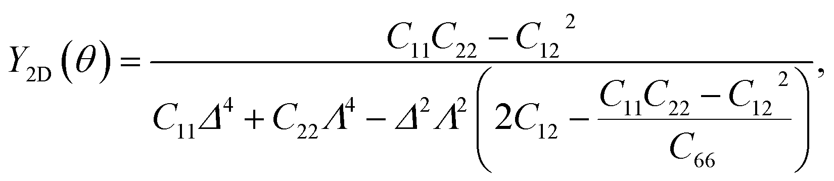 | (2) |
 | (3) |
![[thin space (1/6-em)]](https://www.rsc.org/images/entities/char_2009.gif) sinθ and Λ = cosθ. Here, θ is the angle relative to the armchair direction.
sinθ and Λ = cosθ. Here, θ is the angle relative to the armchair direction.
Due to hexagonal structure, in-plane elastic constant C11 = C22 and we can directly calculate the C66 via relationship C66 = (C11 − C12)/2. It implies that, for C4F2, there are only two nonzero elastic constants to be estimated being C11 and C12.
Our calculated results demonstrate that the in-plane elastic constant of C4F2 being C11 = 499.46 N m−1 and C12 = 55.96 N m−1. The obtained values for the elastic constants of C4F2, as listed in Table 1, satisfies the Born criteria41 for mechanical stability with C11 > 0 and C112 − C122 > 0. Our calculations indicate that the elastic constants of C4F2 are greater than most other 2D layered materials, demonstrating the superiority of its mechanical properties. As listed in Table 1, Y2D = 493.19 N m−1 and G2D = 221.75 N m−1, which is comparable to that of graphene (340 N m−1 and 144 N m−1, respectively).45 Also, the Poisson's ratio of C4F2 is 0.11 which is close to that of graphene (0.17).44 Obtained results for elastic constants reflect that C4F2 has high in-plane stiffness and strong bonding. The polar diagram for the Y2D(θ) and ν(θ) of C4F2 are presented in Fig. 3. We can see that the angle-dependence of Y2D(θ) and ν(θ) of C4F2 have perfectly circular shape, reflecting that C4F2 has fully isotropic elastic properties.
 | ||
| Fig. 3 Polar diagram for the Young's modulus and Poisson's ratio of C4F2. | ||
4 Electronic properties
Graphene and also bilayer graphene are predicted to be semimetal with a zero band gap.46 Surface functionalization is an effective way to turn the electronic properties of layered materials. In Fig. 4, we present our calculated results for band structure of C4F2. Obtained results demonstrated that at the ground state, C4F2 is a direct semiconductor with a large energy gap. Both the conduction band minimum (CBM) and valence band maximum (VBM) locate at the Γ point in the first Brillouin zone. The estimated energy gap of C4F2 by the PBE functional is 4.13 eV, which is larger than that of both graphane (3.5 eV) and fluorinated graphene (3.1 eV).47 However, the PBE method is known to be underestimated the energy gap problem of the semiconductor. Hence, to correct the band structure of the investigated system, we also perform the calculations for the band structure of C4F2 by using the hybrid functional HSE06. Obtained results indicate that the estimated band structures of C4F2 by HSE06 and PBE methods have the same profile. At the HSE06 level, the energy gap of C4F2 is up to 5.75 eV as presented in Fig. 4. To explore the contribution of atomic orbital to the band structure formation, we also plot out the partial density of states (PDOS) as shown in Fig. 4. While the CBM of C4F2 is mainly contributed by F–s orbitals, the VBM is occupied by the C–p and F–p orbitals. The F–p orbital greatly contributes to the valence band, especially in the region from − 3 to − 6 eV. | ||
| Fig. 4 Band structure and partial density of states (PDOS) of C4F2 monolayer. | ||
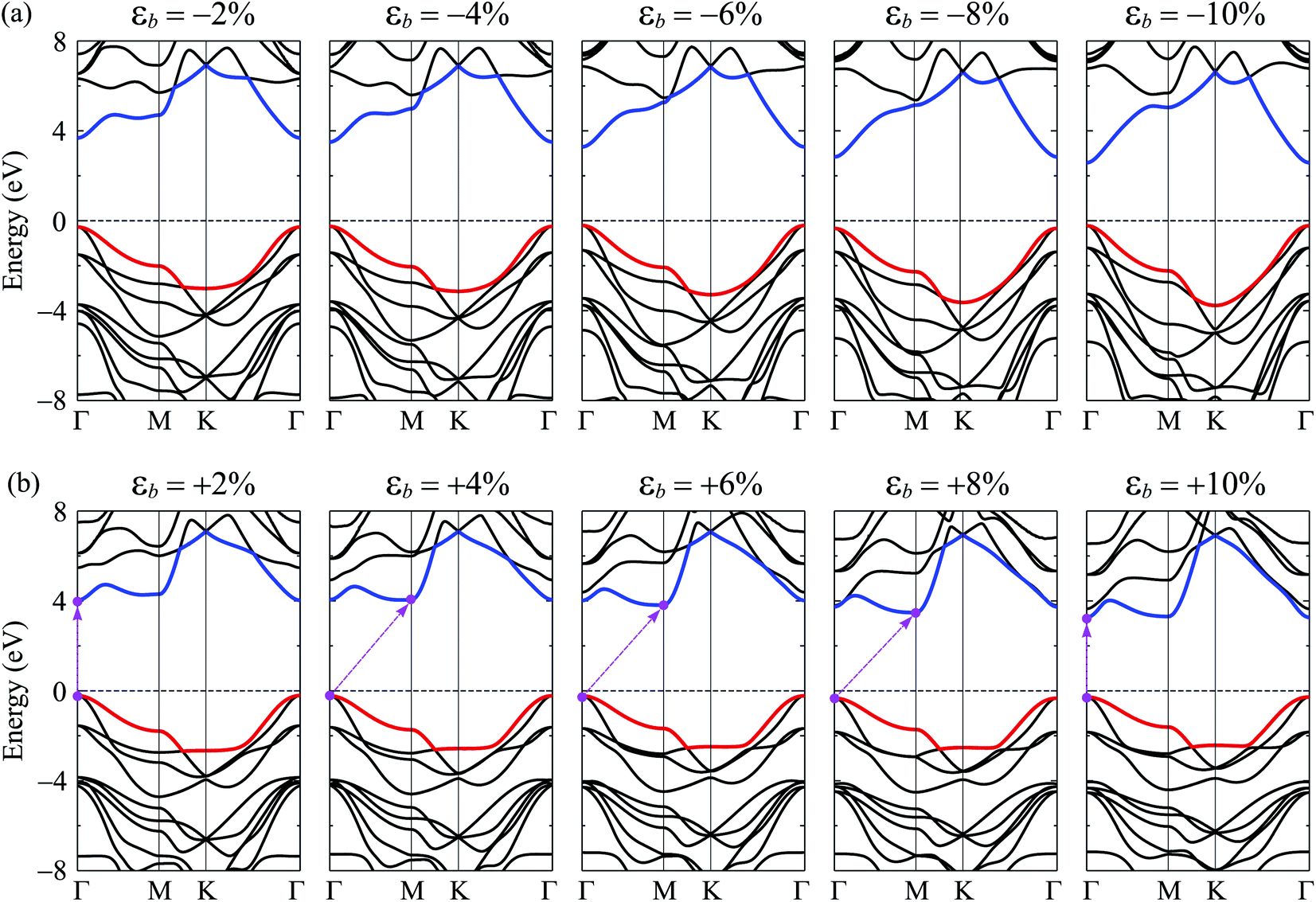
Note that strain engineering is the best way to turn the electronic properties of 2D layered materials. Here, we investigate the dependent-biaxial strain of the electronic properties of C4F2. The dependent-biaxial strain is quantitatively investigated via the expression as εb = (a − a0)/a0. Here, a and a0 are the lattice constants of the investigated system with and without strain, respectively. In the present study, a large range of biaxial strain from −10 to 10% is applied to the system (minus sign stands for the compressive case). Band structure of C4F2 at several values of εb is shown in Fig. 5. In the compressive strain case (εb < 0) as illustrated in Fig. 5(a), direct semiconductor characteristic of C4F2 is preserved, however, its band gap is significantly changed (decreased) when the compressive strain is applied. Interesting takes place in the case of tensile strain (εb > 0) where the direct–indirect gap transitions are observed as illustrated in Fig. 5(b). We can reveal that the CBM tends to move from Γ to M point and vice versa when the tensile strain was introduced. Consequently, the indirect–direct gap transitions take place at εb = + 4% and εb = + 10%. At εb = + 4%, C4F2 becomes the indirect semiconducting material with the CBM at the M-point and the indirect semiconductor characteristic of C4F2 is prevented in the strain range from +4 to +8% and the indirect–direct energy gap transition occurs again at εb = +10% the CBM returns to the original point (Γ-point) and the C4F2 is the direct semiconductor at εb = +10%.
 | ||
| Fig. 5 Band structures of C4F2 monolayer under strain: (a) compressive strain εb < 0 and (b) tensile strain εb > 0. | ||
Along with mechanical strain, the electron states of layered nanomaterials can be modulated by electric gating. In this paper, an electric field E is perpendicularly applied to the surface of investigated material (along c-axes). A plus sign of the electric field E indicates that the ![[E with combining right harpoon above (vector)]](https://www.rsc.org/images/entities/i_char_0045_20d1.gif) direction coincides with the positive direction of the c-axis and vice versa. The band structures of C4F2 under the E are shown in Fig. 6. Obtained results reveal that the band structure of C4F2 depends greatly on the E. In the presence of the E, there is the redistribution of charge due to the electric field and the polarization of effective charges in the electronic bands will also respond to the external field. Consequently, the electron states of materials can be altered by the external field. Obtained results indicate that the transition from semiconducting to metallic behavior is found in C4F2 when the E was introduced. In the presence of the E, the energy gap of C4F2 decreases slightly when the E varies from 0 to 2 V nm−1. However, the energy gap reduces quickly with the continued increase in the electric field. Consequently, The semiconductor-to-metal transitions are found at E = ±5 V nm−1. At E = ±5 V nm−1, as presented in Fig. 6, the highest subband of the valence band and the lowest subband of the conduction band intersect at the Fermi level (the Fermi level is set at zero) and C4F2 becomes a metal. Both the VBM and CBM are always at the Γ-point in the presence of the electric field, implying that C4F2 is a direct semiconductor (except the phase transition point at ±5 V nm−1). The E- and εb-dependent band gap of C4F2 is depicted in Fig. 7. The energy gap of C4F2 decreases quite rapidly (about 32%) in the case of εb < 0, from 4.13 eV at equilibrium (εb = 0) to 2.81 eV at εb = −10%. For the εb > 0 case, the band gap of C4F2 slightly increases and then linearly decreases with tensile strain as shown in Fig. 7(a). The electronic properties of 2D nanomaterials are very sensitive to the altering in their structure. When the strain is applied, the bond lengths between atoms in materials are changed, leading to a change in their hopping energy which plays a key role in the modulation of electron states of materials.48 The semiconductor–metal transition in C4F2 due to the external field as shown in Fig. 6 and 7(b) is an important characteristic that makes C4F2 promising for applications in nanoelectromechanical devices.
direction coincides with the positive direction of the c-axis and vice versa. The band structures of C4F2 under the E are shown in Fig. 6. Obtained results reveal that the band structure of C4F2 depends greatly on the E. In the presence of the E, there is the redistribution of charge due to the electric field and the polarization of effective charges in the electronic bands will also respond to the external field. Consequently, the electron states of materials can be altered by the external field. Obtained results indicate that the transition from semiconducting to metallic behavior is found in C4F2 when the E was introduced. In the presence of the E, the energy gap of C4F2 decreases slightly when the E varies from 0 to 2 V nm−1. However, the energy gap reduces quickly with the continued increase in the electric field. Consequently, The semiconductor-to-metal transitions are found at E = ±5 V nm−1. At E = ±5 V nm−1, as presented in Fig. 6, the highest subband of the valence band and the lowest subband of the conduction band intersect at the Fermi level (the Fermi level is set at zero) and C4F2 becomes a metal. Both the VBM and CBM are always at the Γ-point in the presence of the electric field, implying that C4F2 is a direct semiconductor (except the phase transition point at ±5 V nm−1). The E- and εb-dependent band gap of C4F2 is depicted in Fig. 7. The energy gap of C4F2 decreases quite rapidly (about 32%) in the case of εb < 0, from 4.13 eV at equilibrium (εb = 0) to 2.81 eV at εb = −10%. For the εb > 0 case, the band gap of C4F2 slightly increases and then linearly decreases with tensile strain as shown in Fig. 7(a). The electronic properties of 2D nanomaterials are very sensitive to the altering in their structure. When the strain is applied, the bond lengths between atoms in materials are changed, leading to a change in their hopping energy which plays a key role in the modulation of electron states of materials.48 The semiconductor–metal transition in C4F2 due to the external field as shown in Fig. 6 and 7(b) is an important characteristic that makes C4F2 promising for applications in nanoelectromechanical devices.
 | ||
| Fig. 6 Band structures of the C4F2 in the presence of (a) negative and (b) positive electric fields. | ||
 | ||
| Fig. 7 Band gap of C4F2 as a function of a biaxial strain εb (a) and an electric field E (b). Filled and empty squares in (a) refer to the direct and indirect gaps, respectively. | ||
5 Transport properties
The carrier mobility is a key factor determining possibility applicability of materials to electronic devices. The carrier mobility can be studied by using deformation potential approximation.49 For 2D systems, the carrier mobility μ2D is given by:50,51
 | (4) |
 are the carrier effective and average effective masses, respectively.
The effective mass of the carrier is also an important parameter of materials. The carrier effective mass m* is given by  with E(k) is the electron energy at a wave vector k at the CBM/VBM. Our obtained results show that, at the CBM, the lateral electron effective masses
  along Γ–K and Γ–M of C4F2 are 0.55m0 and 0.55m0, respectively. Here, m0 is the free mass of an electron. Meanwhile, at the VBM, the lateral hole effective masses
  along Γ–K and Γ–M are obtained to be −1.04m0 and −0.97m0, respectively. Consequently, the carrier mobility of C4F2 is predicted to be high due to the low carrier effective masses and high elastic modulus C11. At room temperature of 300 K, the electron mobility μe of C4F2 is found to be 3.03 × 103 cm2 V−1 s−1. Clearly that the electron mobility of our calculated results for the electron mobility of C4F2 is comparable with a previous study (2.73 × 103 cm2 V−1 s−1).52 It is clear that the electron mobility of C4F2 is much higher than that of compounds with similar band gap.53
6 Optical properties
Besides electronic properties, C4F2 possesses interesting optical characteristics that could be useful in performance optical devices. The parameters of optical characteristics can be estimated via the dielectric function, which is written as ε(ω) = ε1(ω) + iε2(ω). Here, ε1/2(ω) and ε2(ω) is the real/imaginary part of ε(ω) at the incident photon frequency ω, respectively. The ε2(ω) is given by54,55
 | (5) |
The absorption coefficient A(ω) is given by57
 | (6) |
The calculated results for the ε(ω) and A(ω) of C4F2 by both PBE and HSE06 approaches are presented in Fig. 8. The static dielectric constant ε1(0) of a semiconductor depends strongly on its band gap. This relationship can be described via the Penn model.58 According to the Penn model, the ε1(0) is inversely proportional to the direct energy gap of the semiconductor. The ε1(0) of C4F2 is 1.53 (PBE) and 1.27 (HSE06). As presented in Fig. 8, there is no absorption in the visible light region. This is due to the large band gap of C4F2 as above-presented. The optical absorption of C4F2 is activated in the ultraviolet region, at 4.13 eV and 5.70 eV respectively by the PBE and HSE06 methods, which is consistent with its direct band gap of C4F2 as above-mentioned. After activation, the intensity of the optical absorption of C4F2 increases rapidly as presented in Fig. 8(b). C4F2 exhibits to have very high absorption intensity in the ultraviolet region. At the PBE level, the maximum absorbance of C4F2 is 6.59 × 105 cm−1 at the incident photon energy of 12.30 eV. It is noted that the Bethe–Salpeter equation (BSE) on top of the one-shot G0W0 calculations (G0W0 + BSE method),47,59,60 which both the electron–electron and electron–hole interactions are taken into account, is considered as the best method to investigate the optical properties of 2D materials. The previous study indicated that the first absorption peak, which is caused by the interband transition, appears at the incident photon energy of 5.47 eV in the absorption spectrum of C4F2 by G0W0 + BSE method.31 These results are comparable to our results by the HSE06 calculations.
 | ||
| Fig. 8 Calculated dielectric function (a) and absorption coefficient (b) of C4F2 by the PBE and HSE06 methods. | ||
7 Conclusion
In summary, we have systematically considered the typical properties of fluorinated diamane C4F2 by using the DFT calculations. Our findings demonstrated that C4F2 is a stable structure with both C–C interlayer and intralayer bond lengths that are similar to C–C bonds in bulk diamond. C4F2 exhibits superior mechanical properties with quite high Young's modulus. Also, C4F2 has high optical absorbance in the near-ultraviolet light region with a maximum value up to 6.59 × 105 cm−1. Interestingly, C4F2 is found to be a semiconductor with a large band gap up to 5.75 eV at the HSE06 level and we can alter its band gap by strain engineering or electric field, especially the semiconductor–metal phase transition is found at E = ±5 V nm−1 which opens up many possibilities for the application of C4F2 in electronic devices.Conflicts of interest
There are no conflicts to declare.Acknowledgements
Sohail Ahmad extends his appreciation to the Deanship of Scientific Research at King Khalid University for financial support through research groups program under grant number (RGP.1/311/42 & RGP.2/188/42).References
- K. S. Novoselov, A. K. Geim, S. V. Morozov, D. Jiang, Y. Zhang, S. V. Dubonos, I. V. Grigorieva and A. A. Firsov, Science, 2004, 306, 666 CrossRef CAS PubMed.
- C. Lee, X. Wei, J. W. Kysar and J. Hone, Science, 2008, 321, 385 CrossRef CAS PubMed.
- B. Hajgató, S. Güryel, Y. Dauphin, J.-M. Blairon, H. E. Miltner, G. Van Lier, F. De Proft and P. Geerlings, J. Phys. Chem. C, 2012, 116, 22608 CrossRef.
- A. H. Castro Neto, F. Guinea, N. M. R. Peres, K. S. Novoselov and A. K. Geim, Rev. Mod. Phys., 2009, 81, 109–162 CrossRef CAS.
- N. A. Poklonski, S. A. Vyrko, A. I. Siahlo, O. N. Poklonskaya, S. V. Ratkevich, N. N. Hieu and A. A. Kocherzhenko, Mater. Res. Express, 2019, 6, 042002 CrossRef.
- A. I. Siahlo, N. A. Poklonski, A. V. Lebedev, I. V. Lebedeva, A. M. Popov, S. A. Vyrko, A. A. Knizhnik and Y. E. Lozovik, Phys. Rev. Mater., 2018, 2, 036001 CrossRef CAS.
- A. D. Phan, N. A. Viet, N. A. Poklonski, L. M. Woods and C. H. Le, Phys. Rev. B: Condens. Matter Mater. Phys., 2012, 86, 155419 CrossRef.
- M. Cao, D.-B. Xiong, L. Yang, S. Li, Y. Xie, Q. Guo, Z. Li, H. Adams, J. Gu, T. Fan, X. Zhang and D. Zhang, Adv. Funct. Mater., 2019, 29, 1806792 CrossRef.
- A. M. Popov, I. V. Lebedeva, A. A. Knizhnik, Y. E. Lozovik, B. V. Potapkin, N. A. Poklonski, A. I. Siahlo and S. A. Vyrko, J. Chem. Phys., 2013, 139, 154705 CrossRef PubMed.
- I. V. Lebedeva, A. M. Popov, A. A. Knizhnik, Y. E. Lozovik, N. A. Poklonski, A. I. Siahlo, S. A. Vyrko and S. V. Ratkevich, Comput. Mater. Sci., 2015, 109, 240 CrossRef CAS.
- F. Schwierz, Nat. Nanotechnol., 2010, 5, 487 CrossRef CAS PubMed.
- G. G. Naumis, S. Barraza-Lopez, M. Oliva-Leyva and H. Terrones, Rep. Prog. Phys., 2017, 80, 096501 CrossRef PubMed.
- K. D. Pham, N. N. Hieu, H. V. Phuc, I. A. Fedorov, C. A. Duque, B. Amin and C. V. Nguyen, Appl. Phys. Lett., 2018, 113, 171605 CrossRef.
- C. V. Nguyen, M. Idrees, H. V. Phuc, N. N. Hieu, N. T. T. Binh, B. Amin and T. V. Vu, Phys. Rev. B, 2020, 101, 235419 CrossRef CAS.
- H. T. T. Nguyen, M. M. Obeid, A. Bafekry, M. Idrees, T. V. Vu, H. V. Phuc, N. N. Hieu, L. T. Hoa, B. Amin and C. V. Nguyen, Phys. Rev. B, 2020, 102, 075414 CrossRef CAS.
- E. Cadelano, P. L. Palla, S. Giordano and L. Colombo, Phys. Rev. B: Condens. Matter Mater. Phys., 2010, 82, 235414 CrossRef.
- A. V. Lebedev, I. V. Lebedeva, A. M. Popov, A. A. Knizhnik, N. A. Poklonski and S. A. Vyrko, Phys. Rev. B, 2020, 102, 045418 CrossRef CAS.
- J. Son, S. Lee, S. J. Kim, B. C. Park, H.-K. Lee, S. Kim, J. H. Kim, B. H. Hong and J. Hong, Nat. Commun., 2016, 7, 13261 CrossRef CAS PubMed.
- L. G. P. Martins, M. J. S. Matos, A. R. Paschoal, P. T. C. Freire, N. F. Andrade, A. L. Aguiar, J. Kong, B. R. A. Neves, A. B. de Oliveira, M. S. Mazzoni, A. G. S. Filho and L. G. Cançado, Nat. Commun., 2017, 8, 96 CrossRef PubMed.
- Y. Gao, T. Cao, F. Cellini, C. Berger, W. A. de Heer, E. Tosatti, E. Riedo and A. Bongiorno, Nat. Nanotechnol., 2018, 13, 133 CrossRef CAS PubMed.
- F. Piazza, K. Cruz, M. Monthioux, P. Puech and I. Gerber, Carbon, 2020, 169, 129 CrossRef CAS.
- S. Rajasekaran, F. Abild-Pedersen, H. Ogasawara, A. Nilsson and S. Kaya, Phys. Rev. Lett., 2013, 111, 085503 CrossRef PubMed.
- D. K. Samarakoon and X.-Q. Wang, ACS Nano, 2010, 4, 4126 CrossRef CAS PubMed.
- L. A. Chernozatonskii, P. B. Sorokin, A. G. Kvashnin and D. G. Kvashnin, JETP Lett., 2009, 90, 134 CrossRef CAS.
- O. Leenaerts, B. Partoens and F. M. Peeters, Phys. Rev. B: Condens. Matter Mater. Phys., 2009, 80, 245422 CrossRef.
- A. G. Kvashnin, L. A. Chernozatonskii, B. I. Yakobson and P. B. Sorokin, Nano Lett., 2014, 14, 676 CrossRef CAS PubMed.
- C. Liu, X. Xu, L. Qiu, M. Wu, R. Qiao, L. Wang, J. Wang, J. Niu, J. Liang, X. Zhou, Z. Zhang, M. Peng, P. Gao, W. Wang, X. Bai, D. Ma, Y. Jiang, X. Wu, D. Yu, E. Wang, J. Xiong, F. Ding and K. Liu, Nat. Chem., 2019, 11, 730 CrossRef CAS PubMed.
- Y. Xie, T. Cheng, C. Liu, K. Chen, Y. Cheng, Z. Chen, L. Qiu, G. Cui, Y. Yu, L. Cui, M. Zhang, J. Zhang, F. Ding, K. Liu and Z. Liu, ACS Nano, 2019, 13, 10272 CrossRef CAS PubMed.
- D. Odkhuu, D. Shin, R. S. Ruoff and N. Park, Sci. Rep., 2013, 3, 3276 CrossRef PubMed.
- J. Sivek, O. Leenaerts, B. Partoens and F. M. Peeters, J. Phys. Chem. C, 2012, 116, 19240–19245 CrossRef CAS.
- H. Shu, J. Mater. Chem. C, 2021, 9, 4505–4513 RSC.
- B. Mortazavi, F. Shojaei, B. Javvaji, M. Azizi, H. Zhan, T. Rabczuk and X. Zhuang, Appl. Surf. Sci., 2020, 528, 147035 CrossRef CAS.
- P. V. Bakharev, M. Huang, M. Saxena, S. W. Lee, S. H. Joo, S. O. Park, J. Dong, D. C. Camacho-Mojica, S. Jin, Y. Kwon, M. Biswal, F. Ding, S. K. Kwak, Z. Lee and R. S. Ruoff, Nat. Nanotechnol., 2020, 15, 59–66 CrossRef CAS PubMed.
- P. Giannozzi, S. Baroni, N. Bonini, M. Calandra, R. Car, C. Cavazzoni, D. Ceresoli, G. L. Chiarotti, M. Cococcioni, I. Dabo, A. D. Corso, S. de Gironcoli, S. Fabris, G. Fratesi, R. Gebauer, U. Gerstmann, C. Gougoussis, A. Kokalj, M. Lazzeri, L. Martin-Samos, N. Marzari, F. Mauri, R. Mazzarello, S. Paolini, A. Pasquarello, L. Paulatto, C. Sbraccia, S. Scandolo, G. Sclauzero, A. P. Seitsonen, A. Smogunov, P. Umari and R. M. Wentzcovitch, J. Phys.: Condens. Matter, 2009, 21, 395502 CrossRef PubMed.
- G. Kresse and D. Joubert, Phys. Rev. B: Condens. Matter Mater. Phys., 1999, 59, 1758 CrossRef CAS.
- J. P. Perdew, K. Burke and M. Ernzerhof, Phys. Rev. Lett., 1996, 77, 3865 CrossRef CAS PubMed.
- J. Heyd, G. E. Scuseria and M. Ernzerhof, J. Chem. Phys., 2003, 118, 8207 CrossRef CAS.
- S. Grimme, J. Comput. Chem., 2006, 27, 1787 CrossRef CAS PubMed.
- T. Sohier, M. Calandra and F. Mauri, Phys. Rev. B, 2017, 96, 075448 CrossRef.
- S. Nosé, J. Chem. Phys., 1984, 81, 511 CrossRef.
- F. Mouhat and F.-X. Coudert, Phys. Rev. B: Condens. Matter Mater. Phys., 2014, 90, 224104 CrossRef.
- Y. Zhang, C.-H. Hu, Y.-H. Wen, S.-Q. Wu and Z.-Z. Zhu, New J. Phys., 2011, 13, 063047 CrossRef.
- N. T. Hung, A. R. T. Nugraha and R. Saito, J. Phys. D: Appl. Phys., 2018, 51, 075306 CrossRef.
- P. Xiang, S. Sharma, Z. M. Wang, J. Wu and U. Schwingenschlögl, ACS Appl. Mater. Interfaces, 2020, 12, 30731 CrossRef CAS PubMed.
- T. Cheng, H. Lang, Z. Li, Z. Liu and Z. Liu, Phys. Chem. Chem. Phys., 2017, 19, 23942 RSC.
- E. McCann and M. Koshino, Rep. Prog. Phys., 2013, 76, 056503 CrossRef PubMed.
- F. Karlický and M. Otyepka, J. Chem. Theory Comput., 2013, 9, 4155 CrossRef PubMed.
- V. M. Pereira, A. H. Castro Neto and N. M. R. Peres, Phys. Rev. B: Condens. Matter Mater. Phys., 2009, 80, 045401 CrossRef.
- J. Bardeen and W. Shockley, Phys. Rev., 1950, 80, 72 CrossRef CAS.
- S. Bruzzone and G. Fiori, Appl. Phys. Lett., 2011, 99, 222108 CrossRef.
- H. Lang, S. Zhang and Z. Liu, Phys. Rev. B, 2016, 94, 235306 CrossRef.
- T. Cheng, Z. Liu and Z. Liu, J. Mater. Chem. C, 2020, 8, 13819 RSC.
- D. Yu, Y. Zhang and F. Liu, Phys. Rev. B: Condens. Matter Mater. Phys., 2008, 78, 245204 CrossRef.
- A. Delin, P. Ravindran, O. Eriksson and J. Wills, Int. J. Quantum Chem., 1998, 69, 349 CrossRef CAS.
- S. Z. Karazhanov, P. Ravindran, A. Kjekshus, H. Fjellvåg and B. G. Svensson, Phys. Rev. B: Condens. Matter Mater. Phys., 2007, 75, 155104 CrossRef.
- H. Wang, G. Qin, J. Yang, Z. Qin, Y. Yao, Q. Wang and M. Hu, J. Appl. Phys., 2019, 125, 245104 CrossRef.
- P. Ravindran, A. Delin, B. Johansson, O. Eriksson and J. M. Wills, Phys. Rev. B: Condens. Matter Mater. Phys., 1999, 59, 1776–1785 CrossRef CAS.
- D. R. Penn, Phys. Rev., 1962, 128, 2093 CrossRef CAS.
- L. Hedin, Phys. Rev., 1965, 139, A796 CrossRef.
- E. E. Salpeter and H. A. Bethe, Phys. Rev., 1951, 84, 1232 CrossRef.
| This journal is © The Royal Society of Chemistry 2021 |