
 Open Access Article
 This Open Access Article is licensed under a
 Creative Commons Attribution 3.0 Unported Licence
Growth of hopper-shaped CsPbCl3 crystals and their exciton polariton emission†
Shiqi Zhao ,
Tong Guo,
Zihao Chu,
Yanping Li,
Wanjin Xu and
Guangzhao Ran*
,
Tong Guo,
Zihao Chu,
Yanping Li,
Wanjin Xu and
Guangzhao Ran*
State Key Laboratory for Artificial Microstructure and Mesoscopic Physics, School of Physics, Peking University, Beijing 100871, China. E-mail: rangz@pku.edu.cn
First published on 26th July 2021
Abstract
CsPbCl3 is an attractive wide-bandgap perovskite semiconductor. Herein, we have grown hopper-shaped CsPbCl3 crystals in a solution droplet dripped on a heated substrate. During the growth, we have observed the impacts of the coffee ring effect and Marangoni flow, which may result in the hopper shape. Their photoluminescence spectra feature double peaks, which are located at 413.9 nm and 422.0 nm, respectively, and the latter increases faster in intensity than the former as the excitation power increases. We believe that the higher-energy peak originates from the excitonic emission and the lower-energy one is from the polaritons' emission, where the polaritons are generated in the exciton–exciton inelastic scattering process. Based on such an explanation, the exciton binding energy of CsPbCl3 is estimated to be 76.7 meV in our experiments, consistent with the previous reports.
Introduction
In recent years, halide perovskites have been intensively studied because of their low-cost solution fabrication process and their outstanding optoelectronic properties. Among them, inorganic perovskites have attracted special attention because of their better environmental stability, especially compared to organic perovskite materials.1–3 As a kind of deep blue light emitting material, CsPbCl3 has been widely studied in lasers4–6 and light-emitting devices.7 But because of the very low solubility of the precursor,8 it is difficult to prepare large sized CsPbCl3 crystals in solution. Furthermore, the surfaces of the growing CsPbCl3 crystals are usually rough due to the spontaneous nucleation and unstable growth when the degree of supersaturation is too high. In order to obtain CsPbCl3 crystals with smooth surfaces, Gui et al. adopted a space-confined growth method and obtained CsPbCl3 microplatelets with sizes of about 30 μm × 60 μm;8 and, by using a similar method, He et al. obtained microdisk arrays of CsPbCl3 for lasing;9 moreover, Hu et al. used soft templates of CH3(CH2)3NH3I micelles in the solution to grow CsPbCl3 crystals.10However, when the degree of supersaturation is finely adjusted at an intermediate degree of the interfacial instability, hopper shapes can form in the surface of the perovskite crystals when grown using a solution method.11–18 Chen et al.,11 Zhang et al.15 and Li et al.17 obtained hopper shaped CH3NH3PbX3 (X = Br, I) perovskite crystals, and attributed it to the dissolution of the crystals due to the low concentration of the precursor in the central part. In the work of Hou et al., the local enrichment of methylamine caused the dissolution of the CH3NH3PbBr3 crystal surface.16 These hopper-shaped crystals are unique in morphologies and usually have some associated properties and applications.19
In this work, we have grown hopper-shaped CsPbCl3 crystals for the first time in a solution droplet dripped on a heated substrate and tentatively clarify the growth mechanism. They have double-peaked photoluminescence (PL) spectra, one of which we attributed to the exciton polariton emission in the inelastic exciton–exciton scattering process.
Experimental section
Materials
PbCl2 (99.99%) and CsCl (99.9%) were purchased from Xi'an Polymer Light Technology Corporation (China), and dimethyl sulphoxide (DMSO, chromatographic grade) from Sigma-Aldrich (USA). The materials were used as received without any further purification.Methods
The precursor solution was prepared by mixing CsCl and PbCl2 with a 1![[thin space (1/6-em)]](https://www.rsc.org/images/entities/char_2009.gif) :1 molar ratio in DMSO solvent, and then the 0.05 M CsPbCl3 precursor solution was stirred at 70 °C for more than 10 hours until the solution became completely transparent. The Si substrate was washed with acetone, ethanol and deionized water, and then transferred onto a heater and preheated at 80 °C. The filtered precursor solution was drop-cast onto the heated Si substrate and maintained at 80 °C for 30 min to let the solution droplet evaporate completely. Finally, the CsPbCl3 crystals were obtained.
:1 molar ratio in DMSO solvent, and then the 0.05 M CsPbCl3 precursor solution was stirred at 70 °C for more than 10 hours until the solution became completely transparent. The Si substrate was washed with acetone, ethanol and deionized water, and then transferred onto a heater and preheated at 80 °C. The filtered precursor solution was drop-cast onto the heated Si substrate and maintained at 80 °C for 30 min to let the solution droplet evaporate completely. Finally, the CsPbCl3 crystals were obtained.
Characterization
Surface morphology images were taken on a high-resolution field emission scanning electron microscope (SEM, FEI Quanta 200F) with an accelerating voltage of 15 kV, also equipped with Energy Dispersive Spectrometer (EDS) and cathodoluminescence (CL). Optical absorption was measured on a UV-VIS-NIR spectrophotometer (Shimadzu UV3600 Plus). PL lifetime was measured on a lifetime and steady state spectrometer (FLS980, Edinburgh, UK). X-ray diffraction (XRD) patterns were measured using X-ray diffraction platform (Model PANalytical X'Pert Pro) with a Cu-Kα radiation source (λ = 0.1541874 nm) at 40 kV and 40 mA. The angle accuracy was within ±0.0025°. PL was excited at 355 nm by a pulsed Nd:YAG laser (pulse width 8.0 ns, repetition rate 1.0 kHz).Results and discussion
Fig. 1(a)–(c) illustrate the growth strategy in a solution phase. As shown in Fig. 1(a), 50 μL of the 0.05 M CsPbCl3 precursor solution is dropped onto an 80 °C Si substrate and the solution droplet forms and begins to evaporate. Because of the sharp wedge-shaped boundary, the droplet evaporates heavier and thus supersaturates first in the boundary regime, and then nucleation and crystallization occur first there. Because of the pinning of the contact line, more and more small CsPbCl3 crystals appear on the contact line and grow up into a few microns scale, forming one circle eventually, similar to the coffee ring. After that, the evaporating droplet decreases in volume and the contact angle becomes smaller as shown in Fig. 1(b). When the contact angle is smaller than the receding angle of the droplet on the Si substrate, the contact line depines and the droplet shrinks abruptly. When the contact line is pinned again, the above growth process will re-occur at the droplet boundary, and the second ring will form. Finally, a pattern with several concentric “coffee rings” is formed as shown in Fig. 1(c) schematically and as demonstrated by the SEM image in Fig. 1(d). The side length of the resulting cubic crystals in the ring regime ranges from 1 to 5 μm. As contrast, the largest crystal locating at the center of the ring is about 50 μm in size with an aspect ratio about 2, and the location of which is related to Marangoni flow as indicated.20 Because the temperature at the vertex of the droplet is lower than other part, the gradient in temperature results in a gradient in surface tension, and finally generates a Marangoni flow in the indicated directions. One CsPbCl3 crystal that originally forms at the droplet boundary is transported to the center of the droplet and drops on the substrate and grows up there. Noticeably, there is a remarkable square depression in the middle of the CsPbCl3 square crystal. The impacts of the substrate temperature and solution concentration are shown in Fig. S1(a–e) in ESI.† The origin of the depression will be discussed in detail later.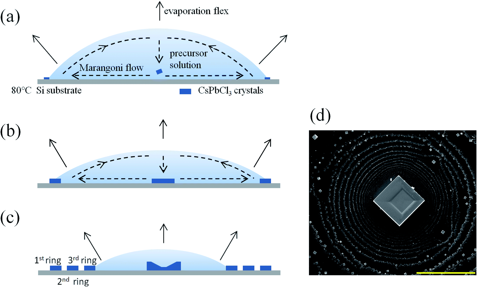 | ||
| Fig. 1 (a–c) Schematic diagram of the growth process for CsPbCl3 crystals. (d) SEM image of a CsPbCl3 crystal and the coffee rings around it. The scale bar is 200 μm. | ||
The SEM image of a typical square crystal with depressions is shown in Fig. 2(a) as an inset, which is grown in the bottom central regime of the droplet and is characteristic of a hopper-shape. The XRD peaks of the crystals shown in Fig. 2(a) at 15.80°, 22.41°, 31.91°, 39.34° and 45.75° can be assigned to (100), (110), (200), (211) and (220) planes of the cubic phase CsPbCl3.21 The EDS spectra of Cs, Pb and Cl shown in Fig. 2(b) confirm the atomic ratio of Cs, Pb, and Cl to be 17.2:20.2:62.6, close to the ratio of 1:1:3 in CsPbCl3. The absorption spectrum of the crystal is shown in the black solid line in Fig. 2(c) and the absorption edge is estimated to be at 413.0 nm. As shown in the blue solid line in Fig. 2(c), the typical PL spectrum of the hopper-shaped CsPbCl3 sample has two peaks at 413.9 nm (peak 1) and 422.0 nm (peak 2) distinctly. The fitted lifetime of peak 1 is 2.9 ns, and that of peak 2 is 1.4 ns as shown in Fig. 2(d), evidently shorter than the former one. The structure and compositions of the central crystal and those in the rings are compared in Fig. S2(a–c), Table S1 and Fig. S3(a–c) in ESI.† It can be seen from Fig. S3(a–c)† that the CL spectra of the central crystals are all double-peaked, and those of rings are all single-peaked, which shows that the double-peaked CL/PL structure is related to the “hopper-shaped” structure.
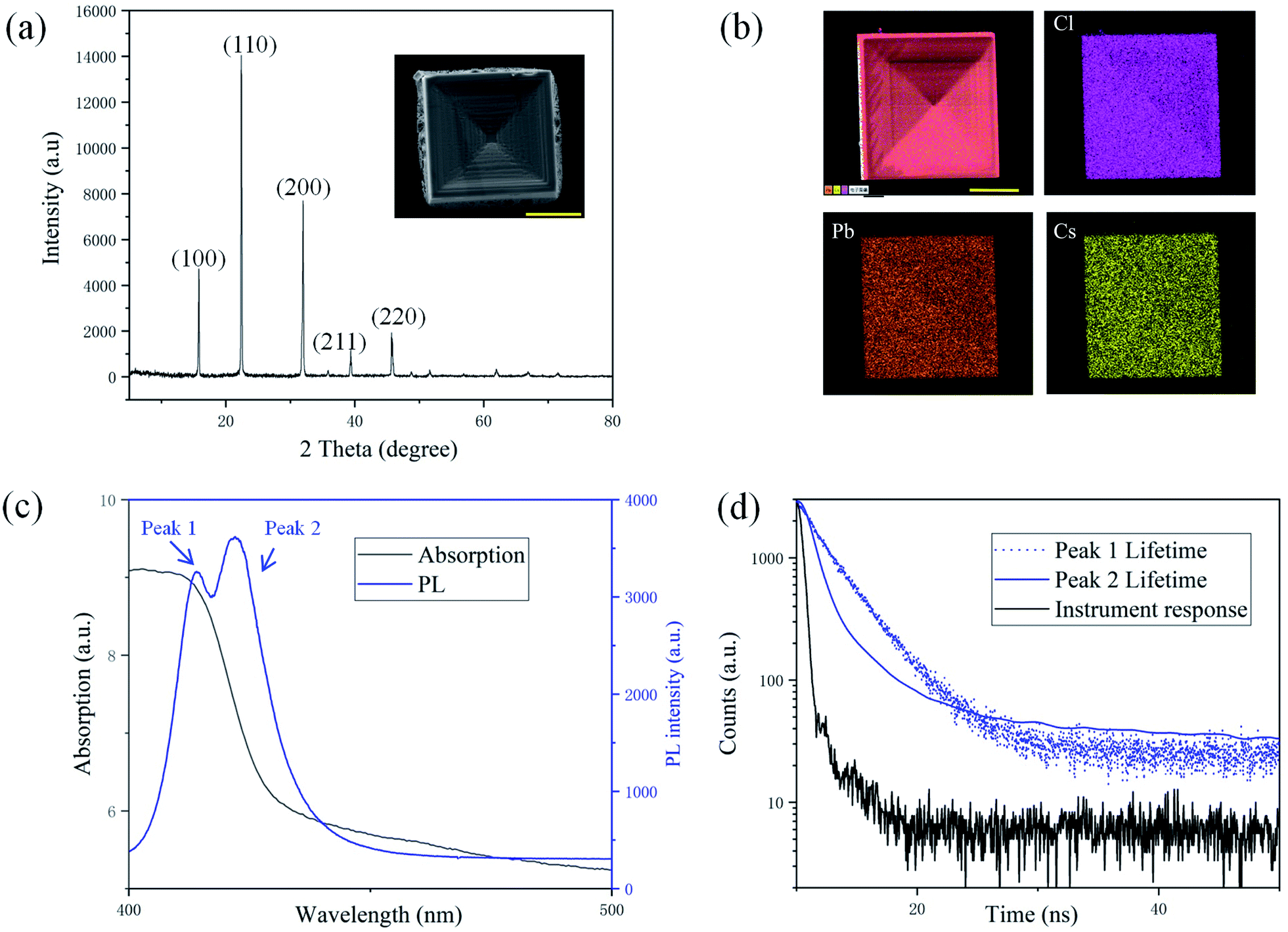 | ||
| Fig. 2 (a) XRD patterns of CsPbCl3 crystals. The inset is the SEM image of a typical CsPbCl3 crystal. The scale bar is 20 μm. (b) EDS mapping images of the CsPbCl3 crystal. The scale bar is 25 μm. (c) The optical absorption spectrum and PL spectrum of the CsPbCl3 crystal. (d) PL lifetime spectra of the CsPbCl3 crystal and the instrument response. | ||
Next, we focus on the growth mechanism of the hopper-shaped CsPbCl3 crystals. The habit of crystal growth is determined by its internal structure and the external growth conditions, such as concentration distributions and temperature. The first factor for the hopper shape is the non-uniform evaporate rate. The precursor solution droplet has a sharp-edged boundary, and thus has a higher evaporation rate there, which can be verified by the diffusion equation.22 As a result, the solution concentration is higher near the boundary, thus the concentration at the edges of the growing crystal is higher than that in the central regime of the crystal, and the growth is faster at the crystal edges. The second factor is the temperature distribution. The precursor solution droplet on the surface of the crystal acts as a heat-insulating layer, thus the temperature in the central regime of the surface of the crystal is higher as indicated by the color map in Fig. 3(a), which is calculated by COMSOL. From the central of the color map to the outer range, the temperature decreases gradually, and the temperature difference is nearly 1 °C in the range of 25 μm. And Fig. 3(b) shows the temperature distribution calculated by COMSOL in the droplet section and around the droplet at the height of the top surface of the grown crystals. The white dotted line indicates the position of the crystal, and the black dotted line shows the intersecting circle of this plane and the droplet. From the central of the color map to the outer range, the temperature decreases about 4 °C in the range of 500 μm. Because the solubility of CsPbCl3 decreases with the decrease of temperature, the degree of the supersaturation is higher around the square crystal and thus it grows faster there. Eventually, the hopper shape, consisting of a series of depression steps, appears on the CsPbCl3 crystal surface as shown in Fig. 3(c). The repeatability of the growth of the hopper shaped crystals is shown in Fig. S5(a–c).†
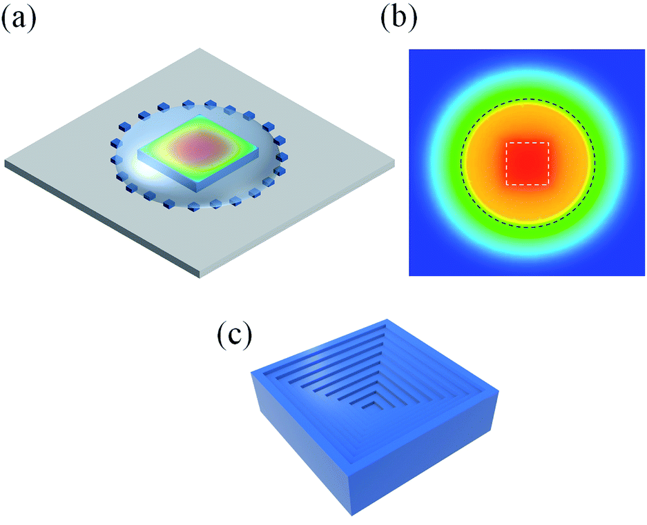 | ||
| Fig. 3 (a) The simulated growth conditions of the hopper-shaped CsPbCl3 crystal. The color map calculated by COMSOL shows the temperature distribution on crystal surface at the height of the grown crystals. From the central of the color map to the outer range, the temperature decrease gradually. The temperature difference is nearly 1 °C. (b) The temperature distribution calculated by COMSOL in the droplet section and around the droplet at the top surface of the grown crystals. The white dotted line indicates the position of the crystal, and the black dotted line shows the intersecting line of this plane and the droplet. From the central of the color map to the outer range, the temperature decreases about 4 °C. (c) The schematic hopper-shaped CsPbCl3 crystal grown in the conditions shown in (a). | ||
Now, we study their double-peaked PL spectra. A series of PL spectra under different pump fluences are shown in Fig. 4(a), and the integrated intensities of peak 1 and peak 2 versus excitation powers are compared in Fig. 4(b). The peak analyses are shown in Fig. S4(a–d).† We can see that the intensity of peak 2 increases much faster than that of peak 1 with the increase of excitation power, similar to the previous reports by Kunugita et al.23 and Chen et al.,24 where the lower-energy PL peak is called polariton-emission. After pumping, the exciton density near the phonon bottleneck regime is so high that they are prone to scattering. After scattering, one exciton is scattered into a higher exciton state with n = 2, and another one is scattered into a photon-like polariton state with lower energy and recombines radiatively there, which is so called polariton-emission.23–28 In our case, peak 1 originates from n = 1 excitons and peak 2 corresponds to polariton-emission, between which the energy difference can be inferred from the transition energy from the n = 1 to the n = 2 exciton state, equal to 3/4 of exciton binding energy.23,27 The energy difference in Fig. 4(a) is 57.5 meV, thus exciton binding energy of the CsPbCl3 crystal is estimated to be 76.7 meV, consistent to the result reported previously.29 With higher excitation level, more exciton scatterings will suppress the increase of exciton emission (peak 1) and enhance that of peak 2, which is the reason for the faster increase of the peak 2 in intensity. The higher exited states (n > 2) of the exciton will relax to lower excited states immediately (∼ps) with the assistance of the phonons at room temperature, thus it is hard to observe the emission from n = 3, 4, etc. in our experiment. In order to further study the optical properties of the crystal, a layer of 50 nm PMMA is spin-coated on the CsPbCl3 crystals grown on glass to prevent exciton quenching when optically excited, then a 200 nm layer of Ag is deposited on the surface by thermal evaporation as a reflector, as shown in Fig. 4(c). In such a microcavity, some weak modes appear, and the mode at 420.9 nm (peak 2m) grows fastest, which exceeds peak 1 in intensity at 3822 μJ cm−2, as shown in Fig. 4(d); however, in the further higher power regime, its increasing rate slows down. Finally, we have examined the PL stability of the crystals in Fig. S6.†
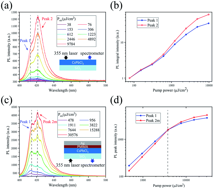 | ||
| Fig. 4 (a) The evolution of PL spectra under different pump fluences. The emitting structure is shown as an inset. (b) The integrated intensities of peak 1 and peak 2 as a function of excitation fluences. (c) The evolution of the PL spectra under different pump fluences. The emitting structure is shown as an inset. (d) The PL peak intensities of peak 1 and peak 2m as a function of excitation fluences. | ||
Conclusions
In summary, we have grown hopper-shaped CsPbCl3 crystals in a solution droplet, and investigated their growth mechanism by comparing the temperature distribution and evaporation rate of the solution droplet. The crystals have double-peaked PL spectra and the peak with lower energy is believed to originate from the exciton polariton emission, and its PL intensity increases faster than that of the other peak with the increase of excitation power.Author contributions
Shiqi Zhao: conceptualization, data curation, formal analysis, software, investigation, validation, visualization, writing – original draft, writing – review & editing. Tong Guo: validation, visualization. Zihao Chu: investigation, validation. Yanping Li: methodology, resources. Wanjin Xu: methodology, resources. Guangzhao Ran: supervision, methodology, project administration, resources, writing – review & editing.Conflicts of interest
There are no conflicts to declare.Acknowledgements
This research is supported by the support of the National 973 program (No. 2013CB632105) and the National Natural Science Foundation of China (No. 11174018).Notes and references
- J. A. Christians, P. A. Miranda Herrera and P. V. Kamat, J. Am. Chem. Soc., 2015, 137, 1530–1538 CrossRef CAS PubMed.
- R. B. Dunbar, W. Moustafa, A. R. Pascoe, T. W. Jones, K. F. Anderson, Y. B. Cheng, C. J. Fell and G. J. Wilson, Prog. Photovoltaics, 2017, 25, 533–544 CAS.
- A. S. Ilin, P. A. Forsh, M. N. Martyshov, A. G. Kazanskii, E. A. Forsh and P. K. Kashkarov, ChemistrySelect, 2020, 5, 6705–6708 CrossRef CAS.
- Y. Fu, H. Zhu, C. C. Stoumpos, Q. Ding, J. Wang, M. G. Kanatzidis, X. Zhu and S. Jin, ACS Nano, 2016, 10, 7963–7972 CrossRef CAS PubMed.
- C. K. Siu, J. Zhao, Y. Wang, D. Yang, X. Xu, S. Pan and S. F. Yu, J. Phys. D: Appl. Phys., 2017, 50, 225101 CrossRef.
- X. Wang, M. Shoaib, X. Wang, X. Zhang, M. He, Z. Luo, W. Zheng, H. Li, T. Yang, X. Zhu, L. Ma and A. Pan, ACS Nano, 2018, 12, 6170–6178 CrossRef CAS PubMed.
- L. Y. Bai, S. W. Wang, Y. W. Zhang, K. X. Zhang, H. Li, K. Ou and L. X. Yi, J. Lumin., 2020, 226, 117422 CrossRef CAS.
- P. Gui, H. Zhou, F. Yao, Z. Song, B. Li and G. Fang, Small, 2019, 15, e1902618 CrossRef PubMed.
- X. He, P. Liu, H. Zhang, Q. Liao, J. Yao and H. Fu, Adv. Mater., 2017, 29, 1604510 CrossRef PubMed.
- X. Hu, X. Wang, S. Zhuang and J. Xu, CrystEngComm, 2020, 22, 178–183 RSC.
- Y. Chen, S. Yang, X. Chen, Y. C. Zheng, Y. Hou, Y. H. Li, H. D. Zeng and H. G. Yang, J. Mater. Chem. A, 2015, 3, 15854–15857 RSC.
- H. R. Jung, G. Y. Kim, B. P. Nguyen, H.-J. Jin, W. Jo, T. T. Thu Nguyen, S. Yoon, W. S. Woo, C. W. Ahn, S. Cho and I. W. Kim, J. Phys. Chem. C, 2017, 121, 21930–21934 CrossRef CAS.
- V. Mohan and P. K. Jain, J. Phys. Chem. C, 2017, 121, 19392–19400 CrossRef CAS.
- Q. Wei, B. Du, B. Wu, J. Guo, M. j. Li, J. Fu, Z. Zhang, J. Yu, T. Hou, G. Xing, T. C. Sum and W. Huang, Adv. Opt. Mater., 2017, 5, 1700809 CrossRef.
- B. Zhang, F. Guo, L. Yang, X. Jia, B. Liu, Z. Xie, D. Chen, H. Lu, R. Zhang and Y. Zheng, J. Cryst. Growth, 2017, 459, 167–172 CrossRef CAS.
- Y. Hou, M. Chen, H. Qiao and H. Yang, J. Energy Chem., 2019, 33, 149–154 CrossRef.
- F. Li, J. Lu, Q. Zhang, D. Peng, Z. Yang, Q. Xu, C. Pan, A. Pan, T. Li and R. Wang, Sci. Bull., 2019, 64, 698–704 CrossRef CAS.
- T. Xu, X. Yang, J. Xing, J. Cheng, H. Yu and Z. Yang, J. Phys. Chem. C, 2020, 8, 6667–6671 CAS.
- Z. Yang, J. Zhang, L. Zhang, B. Fu, P. Tao, C. Song, W. Shang and T. Deng, Adv. Funct. Mater., 2019, 30, 1908108 CrossRef.
- W. D. Ristenpart, P. G. Kim, C. Domingues, J. Wan and H. A. Stone, Phys. Rev. Lett., 2007, 99, 234502 CrossRef CAS PubMed.
- J. Hutton and R. J. Nelmes, J. Phys. C: Solid State Phys., 1981, 14, 1713–1736 CrossRef CAS.
- R. D. Deegan, O. Bakajin, T. F. Dupont, G. Huber, S. R. Nagel and T. A. Witten, Nature, 1997, 389, 827–829 CrossRef CAS.
- H. Kunugita, Y. Kiyota, Y. Udagawa, Y. Takeoka, Y. Nakamura, J. Sano, T. Matsushita, T. Kondo and K. Ema, Jpn. J. Appl. Phys., 2016, 55, 060304 CrossRef.
- M. Chen, X. Shan, T. Geske, J. Li and Z. Yu, ACS Nano, 2017, 11, 6312–6318 CrossRef CAS PubMed.
- H. Ichida, Y. Kanematsu, T. Shimomura, K. Mizoguchi, D. Kim and M. Nakayama, Phys. Rev. B: Condens. Matter Mater. Phys., 2005, 72, 045210 CrossRef.
- M. Bamba, S. Wakaiki, H. Ichida, K. Mizoguchi, D. Kim, M. Nakayama and Y. Kanematsu, Phys. Rev. B: Condens. Matter Mater. Phys., 2015, 91, 235205 CrossRef.
- G. Weng, J. Tian, S. Chen, J. Xue, J. Yan, X. Hu, S. Chen, Z. Zhu and J. Chu, Nanoscale, 2019, 11, 10636–10645 RSC.
- L. Sun, R. Wang, W. Wang, S. Wang, X. Yang and J. Dai, Adv. Opt. Mater., 2020, 106, 110005 CrossRef CAS.
- Q. Zhang, R. Su, X. Liu, J. Xing, T. C. Sum and Q. Xiong, Adv. Funct. Mater., 2016, 26, 6238–6245 CrossRef CAS.
Footnote |
| † Electronic supplementary information (ESI) available. See DOI: 10.1039/d1ra03977f |
| This journal is © The Royal Society of Chemistry 2021 |