
 Open Access Article
 This Open Access Article is licensed under a Creative Commons Attribution-Non Commercial 3.0 Unported Licence
N+-ion implantation induced enhanced conductivity in polycrystalline and single crystal diamond
Dhruba Das and
M. S. Ramachandra Rao*
and
M. S. Ramachandra Rao*
Department of Physics, Quantum Centres in Diamond and Emergent Materials (QuCenDiEM)-group, Nano Functional Materials Technology Centre, Materials Science Research Centre, Indian Institute of Technology Madras, Chennai 600036, India. E-mail: dhrubadas@physics.iitm.ac.in; msrrao@iitm.ac.in
First published on 6th July 2021
Abstract
With the 200 keV N+-ion implantation technique and a systematic variation of fluence, we report on the formation of highly conducting n-type diamond where insulator-to-metal transition (IMT) is observed above a certain fluence wherein the conductivity no longer obeys the hopping mechanism of transport rather, it obeys quantum corrections to Boltzmann conductivity at concentrations of nN ≥ 2 × 1020 cm−3. The conductivity for ultra-nanocrystalline diamond is found to be high, ∼650 Ω−1 cm−1 with thermal activation energy Ea ∼ 4 meV. Interestingly, with gradual increase in fluence, the conductivity in polycrystalline diamond films has been seen to progress from the hopping mechanism of transport in the case of low fluence implantation to a semiconducting nature with medium fluence and finally a semi-metallic conduction is observed where percolation occurs giving an insulator-to-metal transition. XANES confirms that the long-range order in diamond films remains intact when implanted with low and medium fluences; while implantation at sufficiently high fluences >5 × 1016 cm−2 leads to the formation of a disordered tetrahedral amorphous carbon network leading to metallic conduction resembling a metallic glass behaviour. XPS confirms that the sp2 fraction increases gradually with fluence starting from only 6% in the case of low fluence implantations and saturates at 40–50% for implantation at high fluences. A similar observation can be made for single crystal diamond when implanted at high fluence; it retains long-range order but percolative transport takes place through defects or semi-amorphized regions.
1. Introduction
Diamond is considered one of the best next generation candidates of wide-bandgap (WBG) semiconductor materials for high-power high-voltage electronic applications apart from other WBG materials like silicon carbide (SiC) and gallium nitride (GaN) which are known for its higher power throughput, wider frequency bandwidth and higher operational temperatures.1 If we judge diamond based on its physical properties which include high carrier mobilities (electron mobility μe ∼ 2200 cm2 V−1 s−1, hole mobility μh ∼ 2000 cm2 V−1 s−1), high thermal conductivity (20 W m−1 K−1), high breakdown field (10–20 MV cm−1) and a wider bandgap (Eg ∼ 5.5 eV), diamond electronic devices are expected to deliver outstanding performance. Undoped diamond is an extremely good insulator with electrical resistivity ρ > 1015 Ω cm, although its conductivity can be increased by introducing dopants making it p-type or n-type, however the only problem that needs to be addressed is large carrier activation energy of available dopants in diamond for its application at room temperature (RT) for which lower activation energy of dopants is a must. n-Type doping in diamond is possible with donors like nitrogen and phosphorus but the only problem is their large activation energies with Enitrogena = 1.7 eV (ref. 2) and Ephosphorusa = 0.57 eV (ref. 3 and 4) respectively in singe crystal diamond (SCD). Therefore, optimization of the growth conditions for high-purity and high-quality diamond and a possibility of a route for reducing the activation energy of donors by doping via chemical vapor deposition (CVD) or ion implantation process on SCD or polycrystalline diamond is crucial. Although CVD process involves uniform doping while growth with lesser defects (mostly vacancies), still achieving higher electron concentrations giving resistivities like in boron doped diamond (BDD) has been difficult in n-type doping. Large amounts of nitrogen cannot be incorporated effectively in a similar way as in CVD process. Ion implantation is a very effective doping technique which has the capability of precisely controlling the number of implanted atoms of the dopant allowing selective area doping, by which only specific regions with a proper conduction can be fabricated allowing lateral resolution, however, a drawback of this technique is amorphization caused post implantation because of high-energy and high fluence/dose of dopant ions. These kind of damages are usually remedied through post implantation annealing at high temperature and high vacuum.5,6 It has been long known that implantation induced defects in diamond can be annealed by various thermal treatments if the vacancy density is ≤1 × 1022 cm−3 (almost 5% of carbon density in diamond).7–10 Orwa et al.5 on the other hand reported a dramatic and unexpected observation of near-complete annealing of the diamond which was clear from the disappearance of defect peaks at annealing temperatures ∼1423 K. Here annealing did not result in graphitization even at the end of range where the damage was 1.1 × 10²³ vac per cm3 which far exceeded the critical limit. This may be due to the large internal pressures to which the damage structures are subjected within the lattice which constrain them from relaxing to graphite. Nakata et al.11 through atomistic models for ion-beam-induced epitaxial crystallization (IBIEC) had reported that doses of 1–2 × 10¹⁴ P+ per cm2 are quite enough to bring n-type conductivity and restore the lattice after ion impact so that a considerable quantity of P atoms can be incorporated into substitutional sites when annealed. High conductivity has also been obtained in C+-ion implantation12 and O+-ion implantation13,14 in diamond. Although C+-ion implanted layer was graphite like in its electrical conductivity (ρ ∼ 5 × 10⁻³ Ω cm) but it was not like graphite in its mechanical properties. Implanting phosphorus into polycrystalline diamond with fluence 1015 cm−2 confirmed n-type conductivity.15 The conduction mechanism was explained by hydrogen desorption from sp3 clusters during annealing and its diffusion into the sp2 phase in grain boundaries (GBs). The left out dangling bands resulted in smaller sp3 or sp2 carbon clusters adhering to larger ones thereby increasing the diamond amount and it is these diamond sp3 clusters and its doping which resulted in increased conduction although electrons from π bonds in GBs do also provide conductive path. Therefore, it is not just the GB doping which brings in enhanced conductivity but also conduction through effective doping of grains unlike in N doped ultra-nanocrystalline diamond (UNCD).16–18Making n-type diamond with nitrogen has made some success in UNCD via CVD process with the highest conductivity achieved so far is σ ∼ 143 Ω−1 cm−1 where the transport primarily happens by hopping mechanism (NNH or VRH).16,17,19 According to Zapol et al.,20 since UNCD is made of pure sp3 crystals connected with each other through networks of mixture of disordered sp3 and sp2 contents in grain boundaries (GBs), the DFT calculations of nitrogen substitution show that new electronic states associated with carbon and nitrogen in GBs are introduced into the diamond fundamental gap. Ion implantation leads to sp3 bond breakage. These broken dangling bonds introduce mid-gap states which are centered around the Fermi level (EF). These distortions facilitate the incorporation of more nitrogen leading to broadening of π and π* states (created by sp2 bonded carbon atoms). Actually these carbon dangling bond states hybridize with nitrogen lone pairs which lie above EF and donate electrons to the carbon defect states near EF causing it to further shift upward, towards the delocalized π* carbon band with higher doping. Thus, nitrogen doping of the GBs is mainly responsible for higher conductivities in UNCD as nitrogen is preferred more in the GBs than in the lattice.19 It may be noted that GB conduction mechanism was fairly accepted as a reason for enhanced conductivity. However, Dai et al.21 predicted that nitrogen-vacancy center (N-V) can act as shallow donors in diamond lattice thus reducing the activation energy while complexes of nitrogen and dangling bond or nitrogen with a π bond may play the role of compensation centers. We succeeded in obtaining a highly conducting polycrystalline as well as single crystal diamond with N+-ion implantation by systematically varying the fluence/dose. With low fluence, an insulating film is obtained while moderate fluence makes it semiconducting. Similarly, high fluence leads to metallic conductivity and therefore a highly conducting N-implanted n-type layer is obtained in diamond.
2. Experimental details
2.1 Sample preparation
Ultra-nanocrystalline diamond (UNCD) films of grain sizes 3–5 nm were grown using hot filament chemical vapour deposition technique (HFCVD) on Si (100) substrates. Deposition was carried out at 850 °C as substrate temperature and a filament temperature of 2300 °C and chamber pressure of 7 torr was maintained throughout the deposition. CH4 and H2 were used as precursor gases with flow rates maintained at CH4/H2 = 4.5%. Before the deposition, the Si substrate was ultrasonicated with nano-diamond seeds to increase the nucleation. The obtained thickness of the film was ∼3 μm as evident in Fig. 1(c). After the deposition, these first set of samples were then doped with nitrogen using ion implantation technique. A single crystal (SCD) diamond (CVD grown, (001) face-orientation, 2.6 × 2.6 mm, 0.30 mm thick) bought from Element 6 Ltd was also implanted.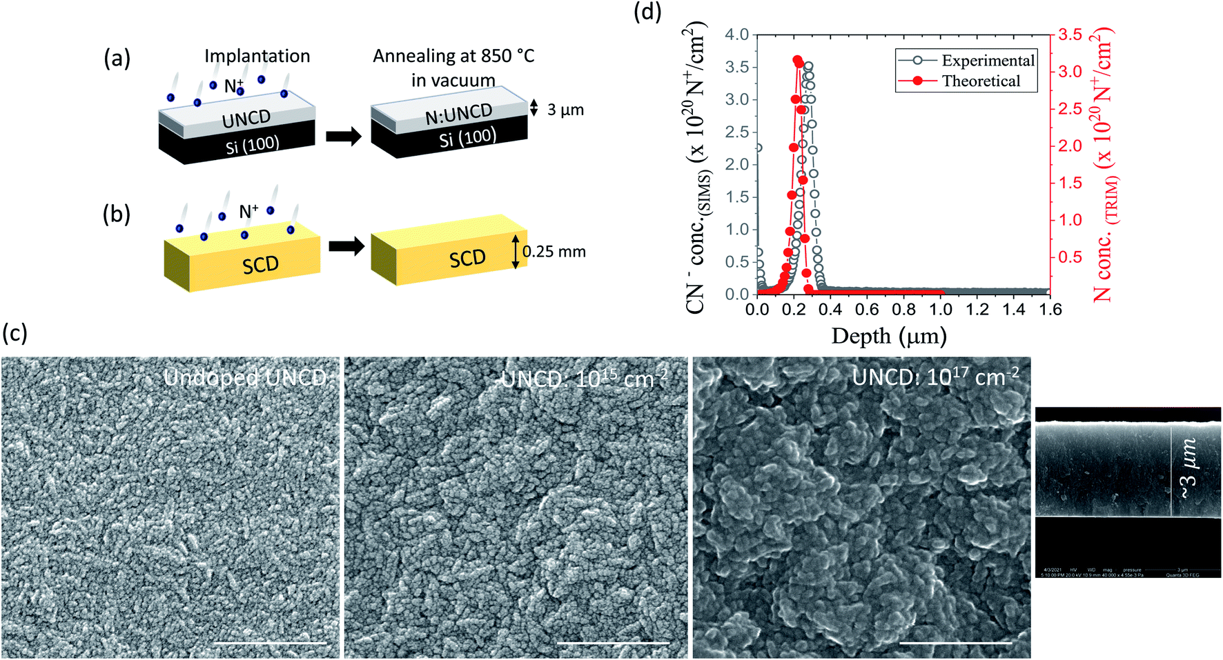 | ||
| Fig. 1 Nitrogen ion implantation. Schematic representation of nitrogen ion implantation process on (a) ultra-nanocrystalline diamond (UNCD) film and (b) single crystal diamond (SCD) and its subsequent annealing procedure. (c) High resolution FESEM microstructure image of undoped and doped UNCD films implanted with low and high fluences of 1015 and 1017 cm−2 respectively (scale bar measures 500 nm) and cross-sectional FESEM image of UNCD film on Si showing film thickness and (d) implanted ion range in UNCD experimentally found out from SIMS and theoretically calculated from TRIM. | ||
2.2 Ion implantation and annealing
Nine undoped UNCD films (1 × 1 cm2, 3 μm thick on Si) grown by HFCVD and one intrinsic SCD sample (2.6 × 2.6 mm2, 0.30 mm thick) were implanted with nitrogen ions (14N+) at low energy ion beam facility with energy 200 keV and beam current 1 μA. The implantation was carried out at room temperature (RT) and different fluences of N+ ions were used in case of UNCD films ranging from 1013 to 1017 cm−2. The SCD sample was implanted with a fluence 1017 cm−2. Post implantation, the diamond films/samples were annealed in vacuum (5 × 10⁻⁶ mbar) at 850 °C for 4 h to mobilize the ions and vacancies inside the lattice as shown in the schematic of Fig. 1. This thermal treatment also enables the host to heal most of the defects caused during implantation with high dose/fluence. The samples were subjected to cleaning in a boiling tri-acid mixture (HNO3![[thin space (1/6-em)]](https://www.rsc.org/images/entities/char_2009.gif) :H2SO4:HClO4 = 1:1:1) and rinsed in a solution of H2O2 + NH4OH and further ultrasonicated in acetone and isopropanol to remove any contamination. Heavy N-doping in single crystal diamond (SCD) via implantation results in the creation of a thin conducting N-implanted layer which resulted in a reduced resistance of 6 × 10³ Ω (by two-probe method) from GΩ values (found in un-implanted diamond); this value of resistance further dropped to 200 Ω after annealing. In order to remove the graphitic/carbon layer on top of the surface, it was etched in tri-acid solution for 5 min only. Since the implantation depth was ∼214 nm, the acid etching could not remove the N-implanted layer. After etching, the two probe resistance was found out to be similar to post annealed condition.
:H2SO4:HClO4 = 1:1:1) and rinsed in a solution of H2O2 + NH4OH and further ultrasonicated in acetone and isopropanol to remove any contamination. Heavy N-doping in single crystal diamond (SCD) via implantation results in the creation of a thin conducting N-implanted layer which resulted in a reduced resistance of 6 × 10³ Ω (by two-probe method) from GΩ values (found in un-implanted diamond); this value of resistance further dropped to 200 Ω after annealing. In order to remove the graphitic/carbon layer on top of the surface, it was etched in tri-acid solution for 5 min only. Since the implantation depth was ∼214 nm, the acid etching could not remove the N-implanted layer. After etching, the two probe resistance was found out to be similar to post annealed condition.
2.3 Sample characterization
The surface morphology of annealed UNCD and SCD films post implantation and annealing were studied by field emission scanning electron microscopy (FESEM) using FEI Quanta 3D SEM and atomic force microscopy (AFM) in non-contact mode and Raman measurements have been undertaken at RT using Witec alpha 300 R spectrometer with lasers of wavelength 457 nm and 532 nm. The structural property was demonstrated using HRXRD (X-ray equipped with graphite-monochromatic Cu Kα radiation (0.15418 nm)), operated at 45 kV and 200 mA. The films were also investigated using X-ray photo electron spectroscopy (XPS) (Specs GmbH, Germany). All spectra were recorded using an Al excitation (Al Kα = 1486.6 eV) source, operated at 10 kV and 10 mA. During acquisition, the base vacuum inside of the analyzer chamber was 3 × 10⁻¹⁰ mbar and operated in a large area mode using a hemispherical energy analyzer. The C K edge X-ray absorption (XAS) spectra were recorded in the total electron yield (TEY) mode by recording a value of sample drain current as a function of the incident photon energy. The electrical transport measurement was carried out in physical property measurement system (PPMS, make Quantum Design Dynacool, USA) in the temperature range (1.9–300 K) and magnetic field (−9 to +9 T) by giving electrical contacts with Al wires using wire-bonder in both four probe and van paw configuration to understand its transport mechanism. The transport properties were measured on annealed samples.3. Results and discussions
3.1 Vibrational and spectroscopic studies on implanted diamond
Fig. 1(a) and (b) depict the schematic of the ion implantation and annealing procedure followed during the experiments wherein N+ ions were implanted with a fixed energy of 200 keV and only the impinging ion's fluence (ions per cm2) was varied during the entire implantation process. As evident from Fig. 1(d), the calculated depth of the implanted ions post implantation was ∼214 nm from the surface found out from simulations using TRIM code22 which matches with the implanted depth found experimentally from secondary ion mass spectroscopy (SIMS) for UNCD implanted at medium fluence. Fig. 1(c) shows FESEM images that reveal the effect of implantation and annealing on the microstructure where it is evident that the UNCD films implanted with low fluence i.e. 1015 cm−2 has same surface morphology as pristine UNCD, while UNCD implanted with fluence of 1017 cm−2 has undergone some sort of surface reconstruction with the grains loosing its well faceted needle like structures when implanted with high enough fluences and annealed afterwards. The grains seem to merge after annealing although no surface damage or defects have been observed, on the other hand the surface morphology of the SCD sample remains the same both before and post implantation. Implantation with very high fluences often brings in amorphization which gets recovered during the process of annealing and the restoration of the crystallinity sets in as we anneal the samples in vacuum at a very high temperature. Fig. 2(a) shows the Raman spectra of the UNCDs implanted with varying fluences (in left panel) and the significant role of annealing in restoring the crystallinity and recovering with lattice defects (in right panel). The Raman spectrum of UNCD implanted with 1013 cm−2 shows no change in its typical UNCD nature excited with 457 nm excitation wavelength. The peaks observable in our UNCD samples, i.e., 1140 and 1330 cm−1, and the overlapping Raman feature from two peaks, 1450 and 1560 cm−1, are characteristic for UNCD (see the deconvoluted spectra in Fig. 2(b)-low fluence). In Fig. 2(b), the peak at 1140 cm−1 (ν1) is due to trans-polyacetylene (t-PA or poly-CHx) at grain boundaries (GBs),23 while the peak at 1450 cm−1 (ν2) represents the mixture of amorphous carbon (a-C) with graphitic content (sp2 phase) at the GBs. The peaks at 1330 and 1560 cm−1 are D and G bands, respectively. D peak is normally interpreted by scattering of disorder activated optical zone-center phonons of A1g symmetry (breathing mode) and G peak is of E2g symmetry for in plane bond-stretching motion of pairs of sp2 carbon atoms.24,25 Due to increased GB volume and sensitivity of the visible Raman more towards sp2-phase, the 1332 cm−1 peak (triply degenerate one phonon diamond peak: T2g mode) is no more observed even in un-implanted ultra-nanocrystalline diamond films. Fig. 2(b) shows the effect of low, medium and high fluence implantations respectively and their deconvoluted spectra before and after annealing. The Raman signature for UNCDs implanted with low and medium fluences are almost similar while for UNCD implanted at high enough fluences (see as-implanted with high fluence spectra in left panel of Fig. 2(b)), it is quite clear that implantation at higher fluences introduces damage in the lattice due to random displacement of atoms that changes the local bonding structure and therefore a broadband feature typical of disordered carbon ∼1550 cm−1 is seen.6,24,26 This is often a signature of tetrahedral amorphous carbon (ta-C) (an amorphous carbon network predominantly rich in sp3 bonding) which when deconvoluted, we get a smaller D band and enhanced G band post implantation.27–29 In Fig. 2(b) (left panel) we observe that the full width at half maximum (FWHM) of D and G band increases upon implantation especially for medium fluence implantations in comparison to low fluence implanted UNCD, but with annealing on same sample at high temperature ∼850 °C (right panel), the D and G band FWHM starts reducing, showing that the crystallinity is somewhat restored and the spectrum almost goes back to its pristine nature of UNCD. However, in case of annealed UNCDs as shown in Fig. 2(b) (right panel), the FWHM of the D peak becomes almost double its value ∼275 cm−1 when implanted with high fluences as implantation induced-disorder increases in the system30 and the spectra reveals more of a ta-C feature which can lead to diffusion of more nitrogen into the lattice. With increasing fluences ranging from low to medium and finally to high, we can see that while the ratio maintains at 1.1 in low fluence region, it starts decreasing slowly in medium fluence regime and finally drops below 1 (0.89 at highest fluence) due to drastically increasing disorder as evident in Fig. 2(c). Implantation causes an increase in sp2 phase in the damaged region and thus can also cause increased sp2 bonding and ordering in GBs31 which leads to gradual movement of G-band towards higher wavenumber also evident in Fig. 2(c) for implanted UNCDs (post annealing). A sudden movement towards higher wavenumber for G band initiates at medium fluence regime and for fluences beyond 1016 cm−2 (high fluence regime), the G-peak position almost saturates at 1595 cm−1 (a signature of increased sp2).
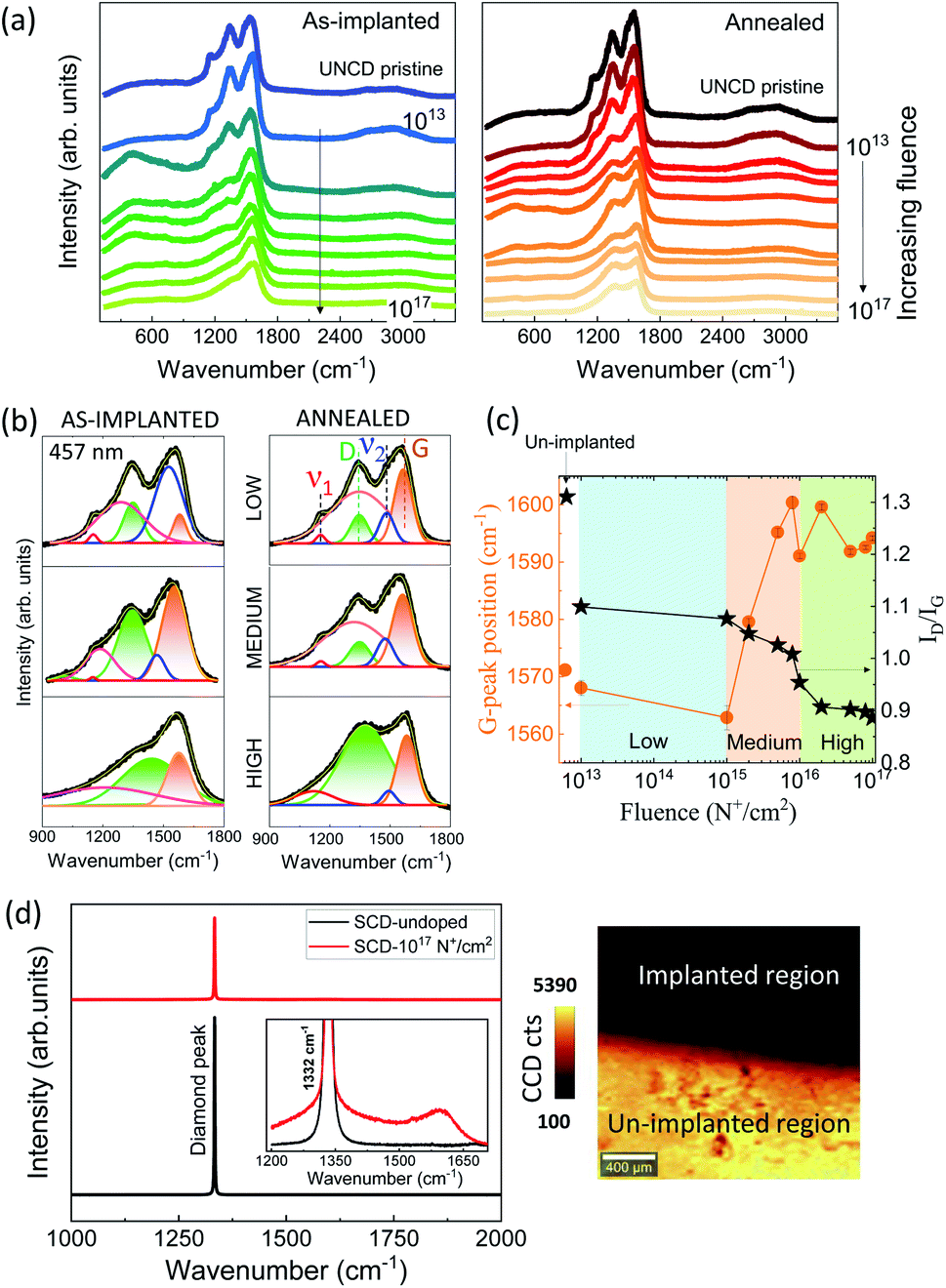 | ||
Fig. 2 (a) Raman spectra for ultra-nanocrystalline diamond (UNCD) films implanted with increasing fluence taken with 457 nm; as-implanted (left) and after annealing (right), (b) deconvoluted Raman spectra for before and post-annealed UNCD samples implanted with low, medium and high fluence respectively, (c) plot of  and G-band position for implanted UNCDs (post-annealing) at different fluences and (d) Raman spectrum for pristine and implanted single crystal diamond (SCD) (post-annealing) showing a weak G-peak at ∼1600 cm−1 compared to un-implanted one and Raman mapping of diamond peak at the implanted and un-implanted region taken with an excitation wavelength of 532 nm. and G-band position for implanted UNCDs (post-annealing) at different fluences and (d) Raman spectrum for pristine and implanted single crystal diamond (SCD) (post-annealing) showing a weak G-peak at ∼1600 cm−1 compared to un-implanted one and Raman mapping of diamond peak at the implanted and un-implanted region taken with an excitation wavelength of 532 nm. | ||
Fig. 2(d) shows the Raman spectra for implanted (post annealed) and un-implanted single crystal diamond (SCD). Diamond implanted with a high fluence of 1017 cm−2 still shows a dominant diamond peak at 1332 cm−1 at all depths throughout the sample although a decrease in intensity is observed with implantation as shown in Raman mapping in Fig. 2(d) (right). The implanted SCD also shows the presence of a very weak G-peak at ∼1590–1600 cm−1 but the relative intensity of the G-peak at 1590 cm−1 (created as a result of implantation/nitrogen doping32) to the diamond peak is very small (the relative intensity only being IG/Idiamond ∼ 0.03). It has been observed that since the radius of C (0.077 nm) atom is comparable to N (0.070 nm) atom, a large amount of nitrogen can be substituted in diamond with comparatively higher fluences where almost all defects created post implantation are expected to be sp3-type bonding defects, that is, “amorphous diamond” defects.11 Therefore, these defects can be annealed almost completely back to the crystalline diamond by only thermal annealing. Although Kalish and co-workers7 predicted that the damage density threshold, beyond which graphitization occurs upon annealing is 1022 vacancies per cm3, for SCD implanted with 1017 cm−2 with almost 20% more vacancies per cm3 in this case, majority of the implanted layer almost anneals back to pristine diamond with annealing at 850 °C. Our results are similar to the work of Orwa et al.5 wherein the Raman line at 1332 cm−1 remains unaffected with an unchanged FWHM of 1.82 cm−1 except for its reduced intensity and its downward shift of ∼0.06 cm−1 w.r.t. un-implanted SCD indicating that there is phonon confinement due to lattice damage that causes skewing and downward shift of the Raman line as previously reported in literature.8 So, we can safely conclude that annealing helps in recovering most of the defects in diamond except for a small percentage of metastable defects remaining due to the motion of interstitials5,11 evident from small peak (at ∼1600 cm−1). Therefore, SCD implanted with high fluence of 1017 cm−2 has not yet undergone complete graphitization upon annealing and thus a thin conducting N implanted layer is produced upon implantation and annealing.
Fig. 3(a) shows the grazing incidence X-ray diffraction (GIXRD) scan of implanted UNCDs after annealing process. We can see the typical XRD peaks of polycrystalline diamond at 2θ = 43.9°, 75.5° and 93.4° for (111), (220) and (311) oriented planes respectively scanned with incident angle ω = 2° (fixed). The GIXRD pattern of implanted UNCDs are exactly similar to pristine one. Fig. 3(b) shows the GIXRD for undoped and doped UNCD just after implantation by varying the incident angle (ω) of X-rays. Since the implantation depth of the buried N-layer is at ∼214 nm; in the GIXRD scan of the highest intensity diamond (111) peak, an adjacent peak starts appearing for ω > 3° and becomes more intense as ω → 10° as the penetration depth of the X-rays increases with increasing ω. This peak has been found to be of hexagonal graphite (101)-orientation or hexagonal carbon (013)-orientation33 which is completely absent in undoped UNCD. The emergence of this peak in UNCD implanted with higher fluences gives clues about the increase in sp2 sites within the buried N-layer. From the Scherrer's formula,34 the mean crystallite size  for UNCD implanted with varying fluences has been calculated for the (111)-oriented planes and plotted in Fig. 3(c) (left). For as-implanted UNCDs, La increases with increasing fluence due to N incorporation which when annealed shows that although the growth of crystallites happens with implantation but after a particular fluence >1016 cm−2, the crystallite sizes decrease. Thus, starts the amorphization or graphitization in the implanted layers at high fluence region with heat treatment. Here the
  ratio is also <1, indicating that amorphization or graphitization has initiated in these films. Fig. 3(c) (right) shows the plot of crystallite size vs.
  For UNCDs implanted with high fluences,
  This relation normally holds for a completely disordered sp2-bonded a-C consisting of distorted sixfold rings or rings of other orders.31 Therefore, following the amorphization trajectory (i.e. increase in sp2%), we could see an increase in crystallite size with N incorporation which peaks at fluence of 1016 cm−2 and gradually falls where the N incorporation is more into sp2 phase bringing disorder into the system.
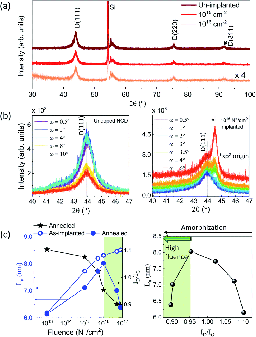 | ||
Fig. 3 (a) GIXRD scan of undoped and implanted UNCDs showing polycrystalline nature of diamond, (b) diamond (111) peak scan with varying incident angle ω from 0.5° to 10° for undoped (left) and implanted UNCD with 1016 cm−2 fluence (right), (c) variation of crystallite size (found out from XRD) for as-implanted and annealed UNCDs and also its corresponding  (post annealing) with implantation fluence (in left panel) and plot of crystallite size versus (post annealing) with implantation fluence (in left panel) and plot of crystallite size versus  for UNCDs (in right panel). The green region denotes the high fluence regime. for UNCDs (in right panel). The green region denotes the high fluence regime. | ||
To verify how much damage has happened in the lattice in case of single crystal diamond and whether a N-implanted layer is indeed formed, we have carried out out-of-plane (004) and in-plane (220) reciprocal space mapping (RSM) of the symmetric and asymmetric peak respectively in case of the implanted SCD and compared it with the un-implanted one. Therefore, ion induced deformations in the implanted layer were measured by XRD. A RSM plot usually shows a distribution of diffraction intensity of one {hkl} point in reciprocal space. RSM of symmetrical (004) out-of-plane reflection of the implanted and un-implanted SCD show no such difference in both the cases shown in Fig. 4(a) and (b) other than an extremely small amount of X-ray diffuse scattering (XRDS) around (004) reflection which is barely visible but a movement of (004) peak towards lower 2θ values is seen meaning an increase in diamond unit cell with N-doping as evident in Fig. 4(c). We carried out the in-plane RSM of the (220) reflection and as evident in Fig. 4(d) and (e) is that the N-ion implantation indeed causes damage mainly for the in-plane (220) planes which is visible in the decreasing intensity of the (220) reflection. Since in the in-plane measurements we are probing a depth of few hundreds of nm (∼300 nm) depth only from the surface as the incidence angle ω = 0.3°, we can safely say that we are probing only that depth up to which the implantation induced damage has occurred. From Fig. 4(f) it is clear that the in-plane reflection is strained due to ion-damage causing an introduction of radiation induced point defects in the implanted layer.
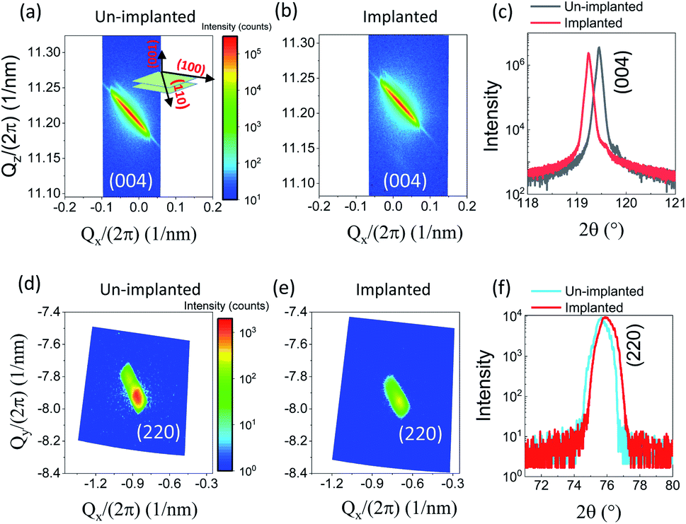 | ||
| Fig. 4 RSM in (a) and (b) out-of-plane mode for the (004) symmetric reflection and (d) and (e) in-plane mode for (220) asymmetric reflection for un-implanted and implanted SCDs respectively and (c) and (f) show the 2θ scan of the (004) and (220) reflection in out-of-plane and in-plane configuration respectively. | ||
As visible Raman spectroscopy is not an ideal method to quantify the sp2 and sp3 fraction because the scattering cross-section for sp2 phase is 50 times more than the sp3 phase, we have carried out the XPS analysis of these implanted UNCD films. Fig. 5(a) depicts the percentage of sp2 present in implanted UNCDs with increasing N doping. Initially the sp2% is less for low fluence implanted UNCDs; it increases from 1.4% to only 6.4%. This fraction gradually increases in UNCDs implanted with medium fluences and can reach upto 40%. On further increase of fluence (in high fluence regime), the sp2 amount reaches in the range 40–49% i.e. almost saturates. This phenomenon is quite expected as with high enough fluences, the diamond lattice is expected to change over to more like tetrahedral-amorphous carbon (ta-C) which was confirmed in X-ray absorption (XAS) studies explained latter in text. In order to look into the distribution of the implanted nitrogen throughout the depths in these implanted UNCD, the XPS N 1s peak scan (at 399.6 eV) was carried out on an as-implanted film by sputtering the film layer-by-layer and is represented in Fig. 5(c). The percentage of nitrogen throughout the depths varied from 0.5% at the surface to almost 9% at the maximum implanted depth as shown in Fig. 5(d). Fig. 5(b) shows the distribution of sp2 and sp3 phases at various depths. Therefore, it is clear from depth-resolved XPS analysis that implantation causes an overall increase in sp2 fraction and that the damage is not uniform throughout the depth instead it peaks at the stopping end-of-range of the impinging ions.
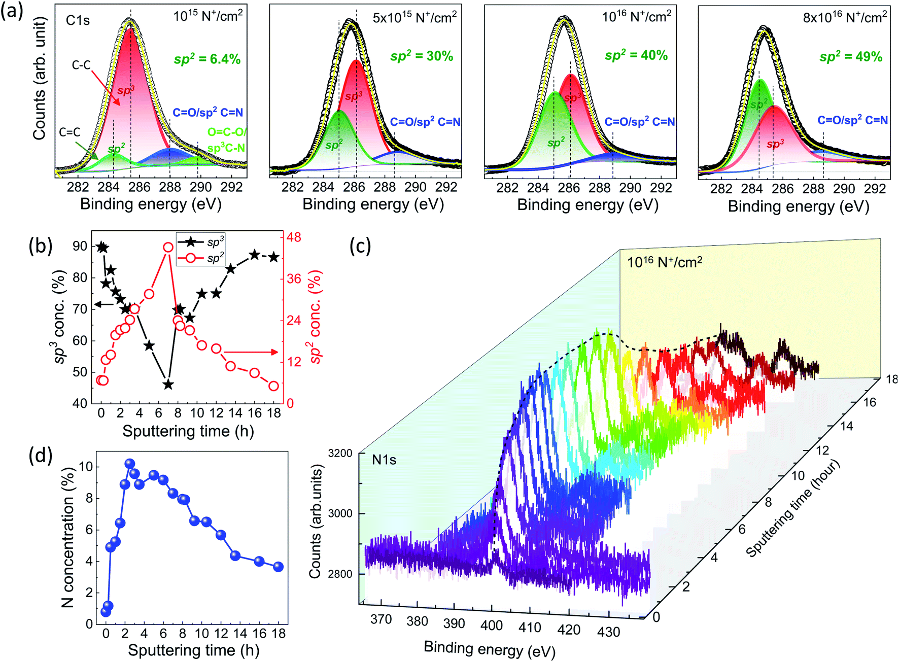 | ||
| Fig. 5 (a) XPS C 1s scan for UNCDs implanted with increasing fluences which shows that in low fluence region, the sp2 amount is quite less <7%, while in moderate fluence the sp2 amount increases drastically to almost 40% and in high fluence regime it saturates in between 40–49%, (b) depth-resolved variation of the sp2 and sp3 fraction in as-implanted UNCD which peaks at implanted range of the N ions, (c) evolution of N 1s peak for as-implanted UNCD at various depths from surface studied by sputtering the UNCD layers by Ar ions and (d) plot of nitrogen concentration present in as-implanted UNCD from surface. | ||
3.2 Transport properties of implanted diamond
Doped semiconductors are the examples where disorder induced by doping caused by potential fluctuations can bring in insulator-to-metal (IMT) transitions.35–37 This transition from insulating to metallic state driven by the basic phenomenon of electron correlation occurs at a critical concentration nc which according to Mott38 occurs when the average spacing between the impurities, nc1/3, is about 4 times the Bohr radius i.e.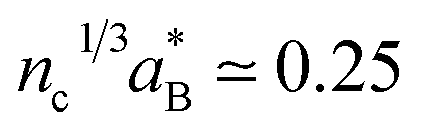 where
where 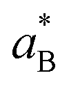 is the effective Bohr radius (shallow state radius). It is very difficult to settle down to fact that whether the observed IMT is induced due to correlation or disorder or a combination of both the phenomenon. The Ioffe–Regel parameter quantifies disorder by the characteristic kFl value, where
 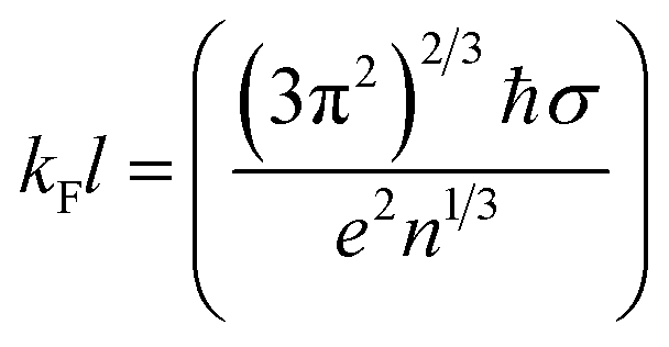 where kF and l are the Fermi wavevector and mean free path length respectively.39,40 It is generally observed that for metallic samples kFl ≫ 1 and insulating samples have kFl ≪ 1. The minimum metallic conductivity of a metal, a concept by Mott, in 3D is given by
 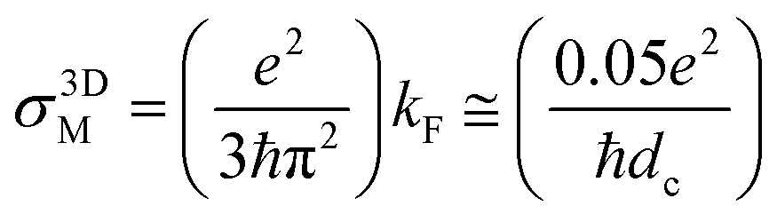 where dc = (nc)−1/3 gives σ3DM ≅ 381 Ω−1 cm−1 and nN ∼ 3 × 1022 cm−3 (theoretically calculated considering EB = 1.6 eV (for nitrogen) and thus
 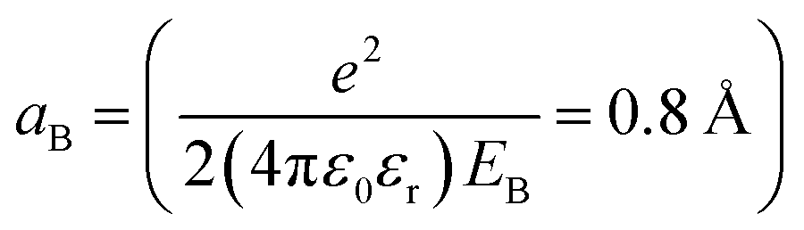 ) for nitrogen doped diamond.
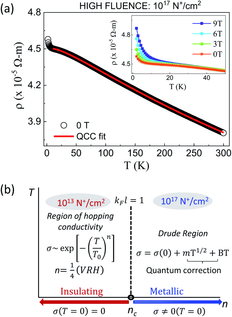
In this article, we report on the observation of IMT and enhanced conductivity in nitrogen-implanted diamond with σRT ≥ 650 Ω−1 cm−1 in case of UNCD films. Fig. 6(a) shows the Arrhenius plots of dc-electrical conductivity of nitrogen implanted UNCDs, where it is evident that nitrogen incorporation leads to an enhanced conductivity wherein the room temperature conductivity values σ300 K and  have been listed in Table 1 for different N+ fluences. The highest obtained conductivity is for UNCD implanted with 5 × 1016 cm−2 as its σ300 K ⋍ 653 Ω−1 cm−1, a much higher value than σ3DM = 381 Ω−1 cm−1 (for nitrogen doped diamond). Carefully plotting resistivity ρ for all the nitrogen implanted UNCDs versus temperature in Fig. 6(b), we can see that the samples implanted with high fluences i.e. >5 × 1016 cm−2 have their low T conductivities greater than σM as denoted with dotted line in the ρ vs. T plot. The inset of Fig. 6(b) shows their room temperature conductivities σRT where it is evident that the conductivity of UNCDs increases from 0.67 Ω−1 cm−1 to 350 Ω−1 cm−1 for implantations in low and medium fluence regime and UNCDs implanted with fluences beyond 1016 cm−2 (high fluence regime) are metallic-like and therefore can be regarded as metallic irrespective of the fact that the ρ dependence on T does not follow a typical metallic behaviour. Therefore, insulator-to-metal transition (IMT) occurs for UNCD doped with nitrogen where electron concentrations are in orders of 1020–1021 cm−3. The samples implanted with low fluences of 1013 cm−2 and 1015 cm−2 lie completely on the insulating side of IMT where their ρ(0 K) → ∞ as T → 0 K in their T dependence. UNCD implanted with high fluences i.e. >5 × 1016 cm−2 have electron concentration ne ≥ 2 × 1020 cm−3 (found from Hall measurements) and therefore show semi-metallic like behaviour with almost a temperature independent resistivity and their
  almost in the range of 0.73 to 0.83.
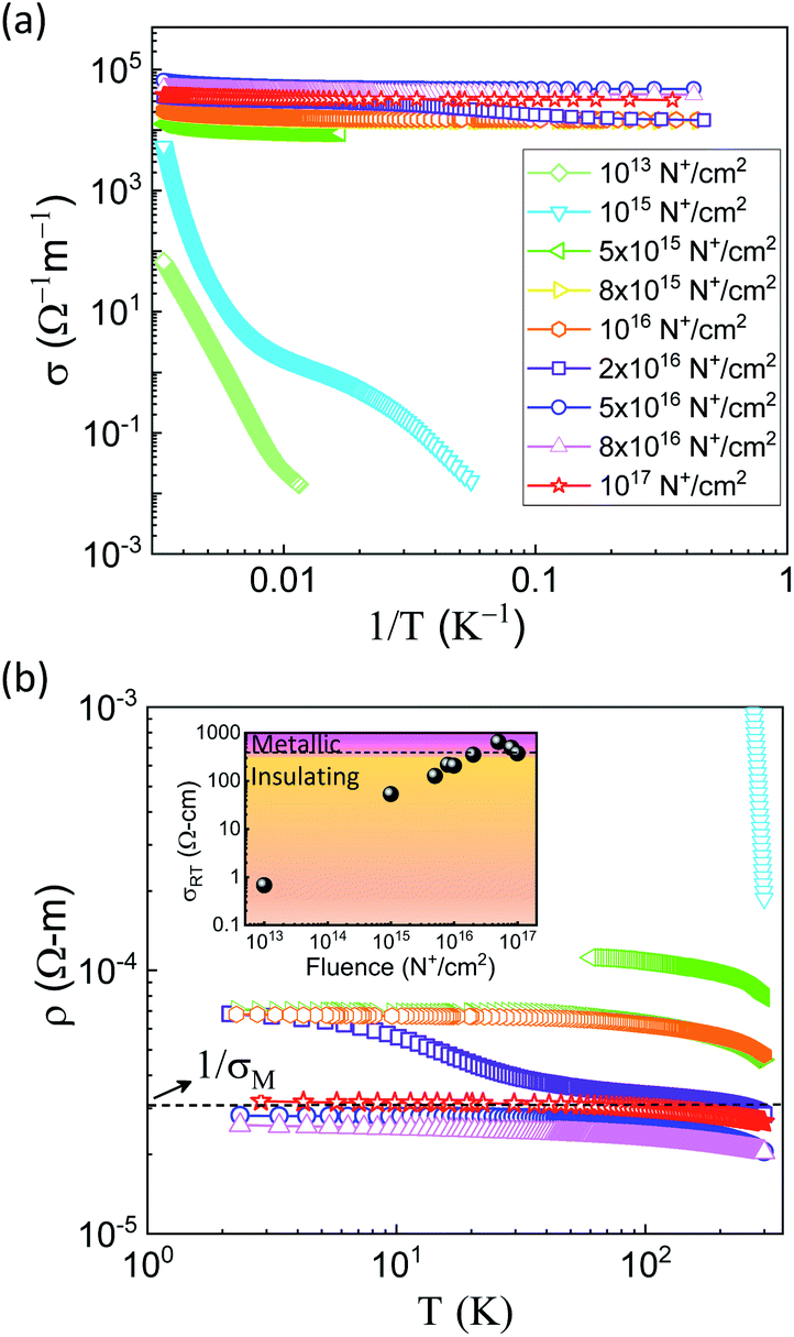 | ||
| Fig. 6 Plot of (a) conductivity versus inverse temperature for UNCDs implanted with various fluences and (b) temperature variation of resistivity depicting that transition from insulating to semi-metallic behaviour of transport property. | ||
| Sample property | Fluence (cm−2) | σ300 K (Ω−1 cm−1) |
|
n (cm−3) (RT) | μ (cm2 V−1 s−1) (RT) |
|---|---|---|---|---|---|
| Insulating | 1013 | 0.67 | — | 5.05 × 10¹⁸ | 0.83 |
| 1015 | 53.23 | — | 7.55 × 10¹⁹ | 4.36 | |
| 5 × 10¹⁵ | 127.29 | — | 1.19 × 10²⁰ | 6.69 | |
| Semiconducting | 8 × 10¹⁵ | 218.24 | 0.65 | 5.69 × 10²⁰ | 2.40 |
| 1016 | 208.79 | 0.70 | 2.90 × 10²¹ | 0.45 | |
| 2 × 10¹⁶ | 354.08 | 0.41 | 9.90 × 10²¹ | 0.22 | |
| Semi-metallic | 5 × 10¹⁶ | 652.71 | 0.73 | 3.97 × 10²¹ | 1.03 |
| 8 × 10¹⁶ | 491.12 | 0.79 | 2.54 × 10²⁰ | 12.08 | |
| 1017 | 376.67 | 0.83 | 4.90 × 10²⁰ | 4.81 |

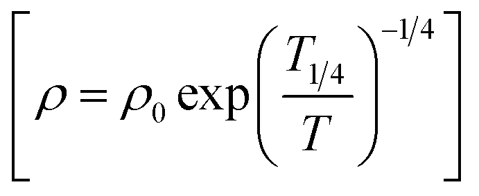 holds good for sample implanted with 1013 cm−2 from 300 K to 100 K evident in Fig. 7(a). Knowing the atomic concentration of nitrogen, the mean distance between nitrogen impurities is given by
 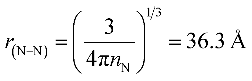 for nN = 5 × 1018 cm−3 (as given in Table 1) and the magnitude of the Coulomb interaction between the nitrogen defects is
 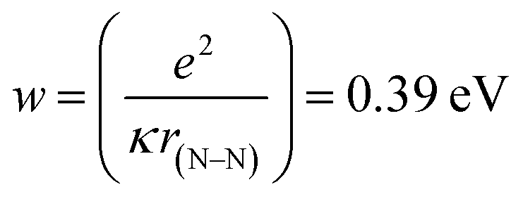 (for diamond, we use the relative dielectric constant κ to be 5.66). The theory of VRH holds assuming a constant DOS in a region extending to several kBT around the Fermi level so that the Fermi level gF is given by
 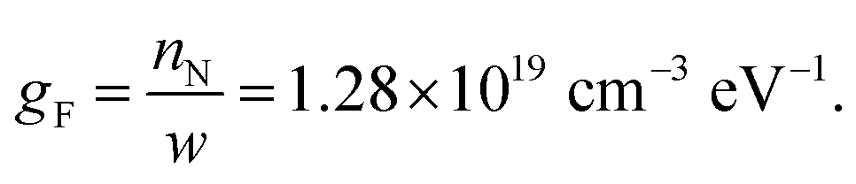 Using
Using  fitted in Fig. 7(a) to the experimental data using T1/4 as a variable parameter, we obtained (T1/4)exp1/4 = 111.98 K1/4, however the theoretical value of T1/4 is given by
  where localization length
  is taken as
  found from experimental T1/4 value
 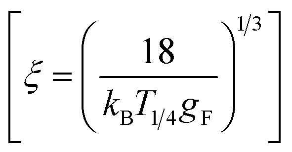 and therefore (T1/4)theoretical1/4 = 60.58 K1/4, almost comparable to experimental value. This hopping conductivity is due to electrons hopping in between defect centers created as a result of nitrogen forming bonds with the C dangling bonds which introduce impurity bands near the Fermi level.20 With more nitrogen getting into the system in medium fluence regime, this band broadens and overlaps with π* and σ* bands of sp2 carbon sites in the diamond bandgap and thus it moves towards the conduction band decreasing the activation energy and therefore semiconducting nature of conductivity values are obtained. Fig. 7(b) shows the temperature dependent Hall measurements whose negative slopes confirms that the electrons are the majority carriers whose concentration matches the SIMS data of Fig. 1(d) and respective mobilities are almost temperature independent. Also the mobility of these carriers in medium fluence regime cannot be explained by the conduction through grain boundaries as the amorphous carbon constituting the GBs when doped can exhibit a mobility value41,42 ∼10−6 cm2 V−1 s−1; values very less than the obtained values in present case (μe ∼ 0.2 cm2 V−1 s−1) along with enhanced conductivity (σ ∼ 300 Ω−1 cm−1) which is only possible in case of actual doping in diamond grains as well apart from just GB doping. Beloborodov et al. had compared the two characteristic lengths i.e. screening length re and localization length ξ and predicted that the crossover from insulating to semi-metallic regime of transport occurs for re ∼ ξ which happens at a critical electron density
 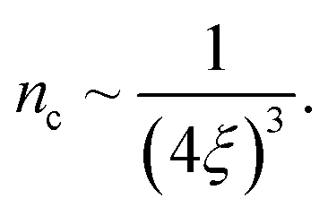 43 Thus, transition from hopping to degenerate semiconductor type behaviour should occur when nc ∼ 2 × 1020 cm−3 for ξ ≃ 4.7 Å in our system. This value of nc agrees well with our experimental results. We calculated the mean hopping distance at 100 K as
 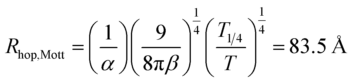 where β = 5.7 and the average energy needed for this hop is given by
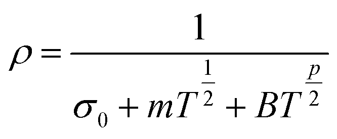
 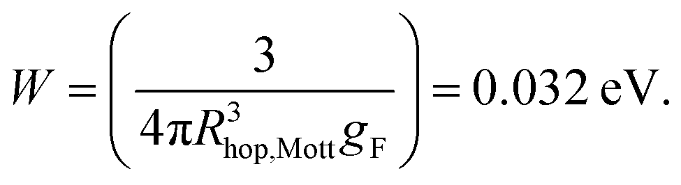 This means here W > kBT and αRhop,Mott = 17.8 i.e. αRhop,Mott > 1 which are in good agreement with the hopping type conduction to account for the insulating UNCD implanted with 1013 cm−2. Hence, this hopping mechanism of transport is taking place for kFl = 0.02, i.e. kFl ≪ 1 (on insulating side), however what happens when the carrier concentration increases which makes kFl > 1. In order to understand that, we have plotted the ρ vs. T plot of UNCD implanted with highest fluence possible i.e. 1017 cm−2 in Fig. 8(a).
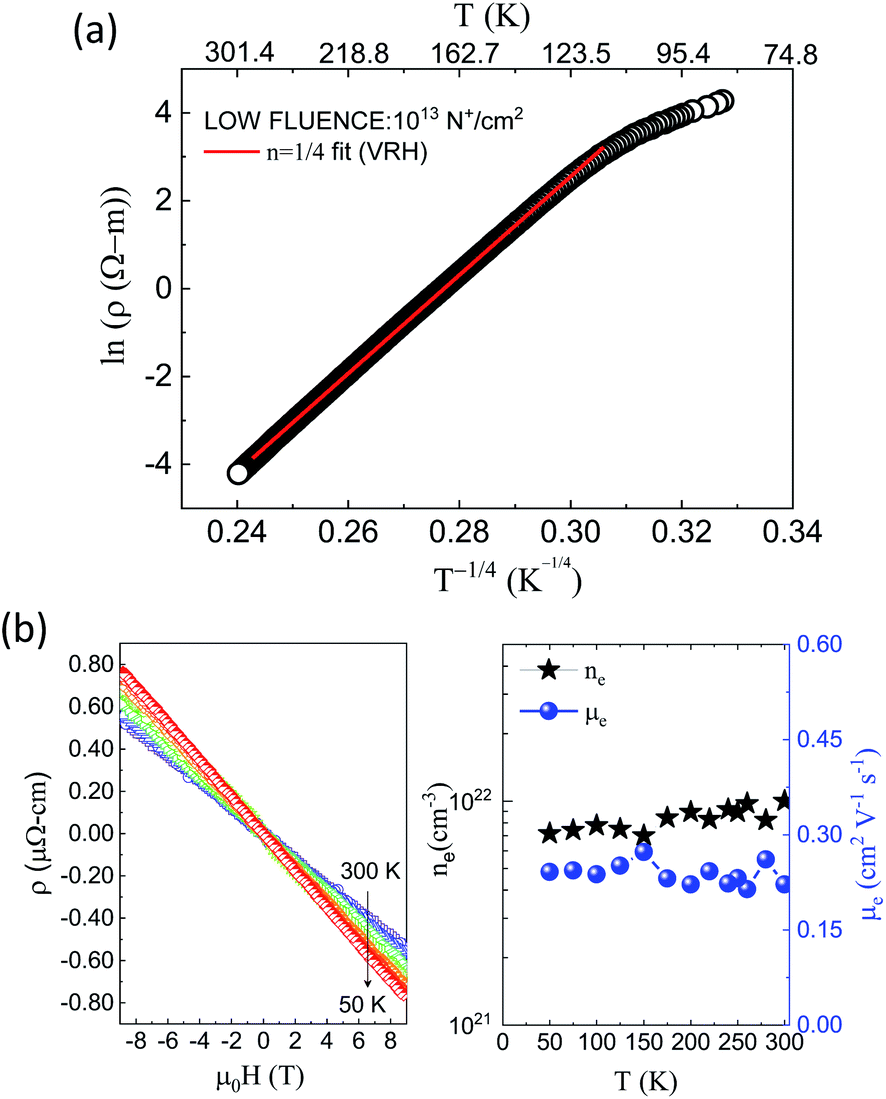 | ||
| Fig. 7 (a) lnρ vs. T−0.25 plot for UNCD implanted at low fluence showing insulating behaviour and exhibiting VRH mechanism of transport, (b) Hall resistivity vs. applied field (left) showing n-type conduction and the corresponding electron concentration and its respective mobility at various temperatures (right) for UNCD implanted at medium fluence which is semiconducting in nature. | ||
 | ||
| Fig. 8 (a) Resistivity versus temperature plot for UNCD implanted with high fluence i.e. 1017 cm−2 (semi-metallic) where the QCC (quantum corrections for conductivity model) fits properly from 300 K to 10 K and below 10 K and (b) a schematic illustration of the conduction mechanism in UNCDs with various ion fluences. | ||
 | (1) |
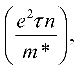 mT1/2 gives the coulombic electron interaction and BTp/2 is the contribution from weak localization due to self-interference of wavefunctions backscattered on nitrogen impurities, p depends on the nature of interaction (2 for electron–electron and 3 for electron–phonon interactions). For UNCD implanted with high enough fluence ∼1017 cm−2 (kFl = 1.88, nN = 4.90 × 1020 cm−3), the ρ vs. T fits well with QCC model from 300 K down to 10 K with the parameters as σ0 = 355.85 Ω−1 cm−1, m = −299.95, B = 53.6 and p = 2. As already mentioned when the Fermi level lies in a region with high density of states (DOS) that are introduced due to ion impact in diamond bandgap; mostly the π defect states due to carbon sp2 phase, the electron wavefunction tends to be delocalized and a quasi-metallic behaviour of conductivity sets in with negative temperature dependence of resistivity. This resembles the “Fermi glass type conduction” often observed in heavily doped/compensated semiconductors or amorphous semiconductors and their alloys where the degree of disorder is high.44,45 Therefore, EEI and WL start playing major roles when kFl ≥ 1 whereas VRH remains the dominant path for electron transport in case of kFl ≪ 1 behaving as an Anderson–Mott insulator schematically depicted in Fig. 8(b).
If we carefully look into the values of the activation energies derived from the slope of the straight line fit in lnρ vs. T−1 plot, the activation energy (Ea) in case of these nitrogen doped UNCD varies from 0.44 eV to 4.05 meV (300–260 K) for UNCD implanted with low fluence and high fluence respectively, very less in comparison to reported value for nitrogen (Ea = 1.7 eV), being a deep donor below the conduction band.2,46,47 These reduced Ea values with increasing nitrogen concentration supports the observation of high conductivity in nitrogen doped diamond which could be due to defect states created as already mentioned and its broadening with electronic wavefunctions sufficiently overlapping leading to percolative conductivity. IMT observed in nitrogen implanted UNCD is very interesting from the point of view of the fact that till now it had been known that conduction process in nitrogen doped diamond film is due to GB doping only where nitrogen is mostly preferred in grain-boundaries (GBs) making it n-type.16,20,21,43 We should remember that for low to moderate fluences till 2 × 1016 cm−2, we see a an insulating to weakly-insulating or semiconducting behaviour which mostly obeys hopping mechanism of transport. In this region, the implanted UNCDs have not yet undergone graphitization upon annealing and although the sp2 fraction has increased up to 40%, the obtained mobility values do not agree with the conduction through doped sp2 carbon present in GBs. Recently in phosphorus implanted UNCDs, we could see signatures of band conduction at temperatures >200 K where a two-channel conduction process is observed; one through the impurity or defect band and the other being the conduction band.48 The electron mobility values obtained in medium fluence regime for N:UNCD are ∼0.2 cm2 V−1 s−1, almost matching with the mobility of the impurity band electrons reported in P:UNCD. For UNCDs implanted with high fluences (>5 × 1016 cm−2), the transport falls in the Drude region where QCC model comes into picture. These UNCDs have sp2 fraction >40% and have undergone amorphization and thus are semi-metallic. The transport here is mainly through these increased amorphous-sp2 networks.
Heavy N-doping in single crystal diamond (SCD) via implantation results in the creation of a thin conducting N-implanted layer. Fig. 9(a) represents the ρ vs. T and its field dependence plot for SCD implanted with 1017 cm−2. Here also interestingly the transport properties can be described using quantum corrections to Boltzmann equation given by QCC. The resistivity decreases monotonically with temperature i.e.  is always negative and reaches a maximum and then again reduces with positive temperature coefficient of resistivity at lower temperatures like previously reported in many graphitized carbon systems49–52 which seems to originate from decrease of electron–phonon scattering. IMT is observed in the temperature dependence of ρ starting from 300 K down to 2 K with the temperature at which transition from insulating to metallic regime occurs being TIMT = 44.5 K. This temperature defines the boundary for the two kinds of contribution: localization (σ ∝ T) and interaction (σ ∝ T1/2) where localization prevails in the higher temperature regime and interaction effects due to impurity scattering dominate at lower temperatures. This kind of transport phenomenon mainly the weak localization has also been reported in oriented graphite but at very low temperatures (<1 K)53 while the occurrence of the electron–electron interaction is quite evident in disordered metallic glasses.44,54 The room temperature resistivity ρ300 K = 8.2 × 10⁻³ Ω m is very low compared to un-implanted SCD (the resistance for undoped SCD is in GΩ limits) and
  of nitrogen implanted SCD is 1.02 indicating a semi-metallic nature with an activation energy Ea = 2.35 meV (at 280–300 K). Although the ρ vs. T dependence of SCD is similar to that of polycrystalline graphite, there is a marked difference amongst them when it comes to their magnetoresistance properties. We carried out the temperature dependence of magnetoresistance
 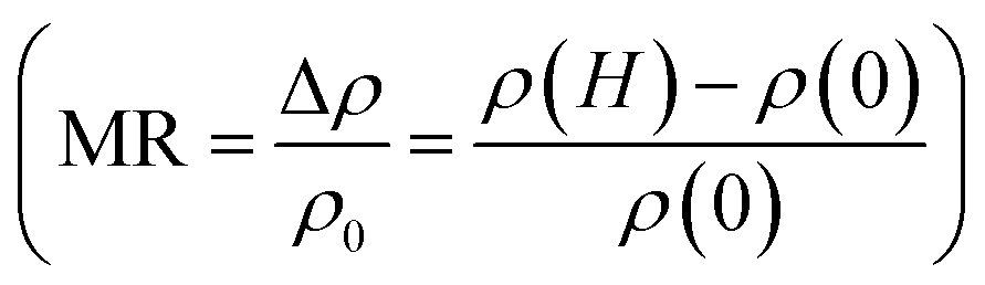 and plotted in three different plots to show the contribution of different effects at different temperature regimes in Fig. 9(b)–(d). We already know that there is a temperature correction to σ0 which is positive for the localization model and negative for Coulomb interaction model. Application of magnetic field therefore should give important clues about the magnitudes of these two contributions. At temperatures less than TIMT, a positive magnetoresistance due to interaction effects is observed which can be elucidated by two band conduction model55,56 i.e. conduction in two bands of differing conductivities and mobilities caused by the application of magnetic field which induces a change in relative population in conduction band and impurity band. The experimental MR data fits well with two band conduction model given by,
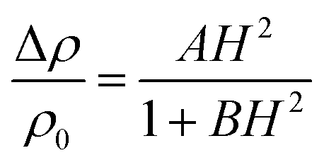 | (2) |
 of approximately 2% is observed at 2 K and at 9 T field. An anomalous negative MR at temperatures above TIMT is a signature of the dominance of the localization effects (although very small in this case
  ).61,62 The experimental data fits with a semiempirical expression given by Khosla and Fischer which is of the form63
 | (3) |
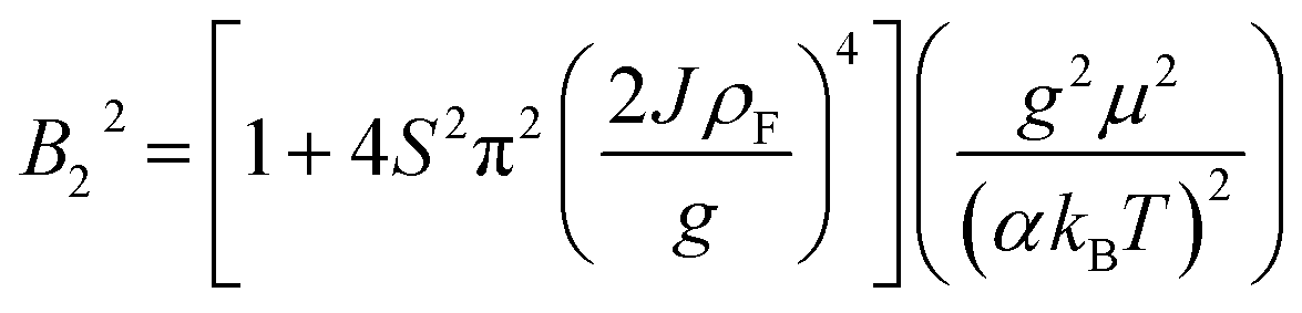 where the parameter
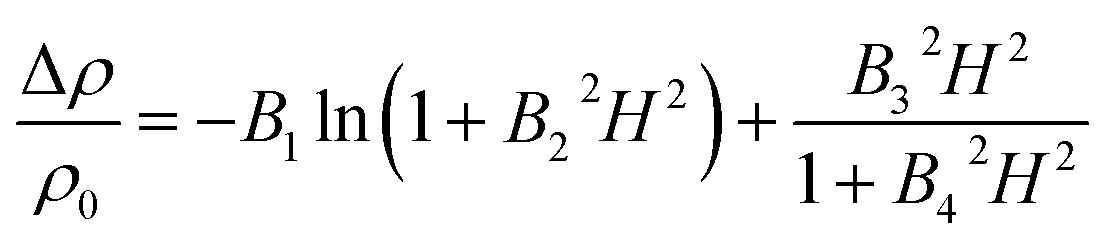
 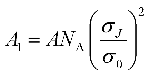 a measure of spin based scattering; A is a numerical constant, NA is Avogadro's number, σJ and σ0 are the scattering cross-sections due to exchange interaction and other mechanisms respectively. J is the exchange integral, ρF is the density of states at the Fermi level, S is the spin of the localized magnetic moment, 〈M〉 is the average magnetization, g is the g factor, and α is a numerical constant. This kind of negative MR was first reported in n-type Ge64 and also in pregraphitic carbon fibres.53,65 If we see the MR in the transition region around TIMT, we see that the experimentally observed magnetoresistance is negative at low field then passes through a minimum before finally becoming positive at higher field owing to admixture of the positive component. In order to fit this data, we have used the compound expression involving both positive and negative contributions to MR given by the compound expression63,66 (eqn (2) + (3))
 | (4) |
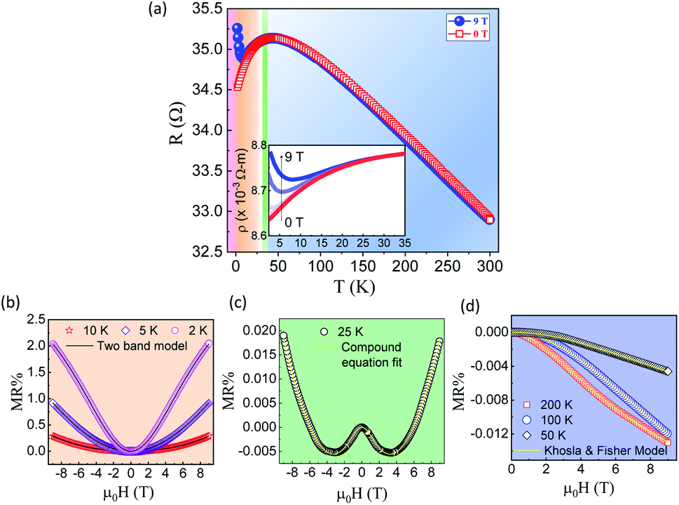 | ||
| Fig. 9 (a) Plot of resistivity versus temperature for single crystal diamond (SCD) implanted with fluence 1017 cm−2 showing an insulator-to-metal transition in its temperature dependence marked by transition from blue to red region with TIMT = 44 K, magnetoresistance (MR) data at the various temperatures/regions of the insulator-to-metal transition (IMT): (b) metallic side (below TIMT) showing positive MR, (c) at transition region (25 K) showing transition form negative to positive MR and (d) at the insulating side (>100 K temperatures) showing negative MR and their corresponding fits. | ||
3.3 X-ray absorption studies of implanted diamond
We performed the X-ray absorption near-edge structure (XANES) study of implanted diamond (both polycrystalline and single crystal) to study the implantation induced local structure modifications in chemical bonding and defects creation with increasing ion fluence. The doses were varied from low (1013 to 1015 cm−2) to moderate (1015 to 1016 cm−2) and finally to high fluence (>1016 cm−2) to study damages ranging from point defects (in case of low fluences) to high density of defects/disorder (for moderate fluences) and ultimately leading to partial or complete graphitization (at high fluence). In XANES, diamond displays an absorption edge corresponding to the C 1s core exciton at 289.3 eV, about 0.2 eV below the conduction band minimum67–70 and a characteristic second bandgap i.e. a dip at 302.5 eV.71 It also displays a weak peak at ∼285 eV (C(1s) → π*) which is also a common feature of both a-C and graphite due to small sp2 defects. Along with all these, a peak at 287.5 eV is also observed assigned to C(1s) → σ*(C–H) resonance.72 In Fig. 10(a) these features are resolved in polycrystalline diamond (UNCD) implanted with low to moderate fluences and also in single crystal (100) diamond. From Fig. 10(b), it is clear that for low to moderate fluences no significant damage to the diamond long-range order is observed as evident from the absorption in the range 290–310 eV. The XANES data clearly indicates that the sp2 π* absorption due to localized sp2 configurations present in GBs increases gradually as the implantation fluence increases. This increase in sp2 contribution was also confirmed from XPS data where we quantified the sp2/sp3 ratio. A gradual decrease in C–H resonance (a shoulder peak at 287.5 eV) is also seen with implantation. An overall increase in π* resonance combined with decrease in C–H resonance which quantifies the amount of sp3 content in sample indicates the formation of more of the sp2 localized states preferentially at the GBs. The diamond core exciton seems to be most sensitive to implantation and therefore its reducing intensity denotes the decreasing crystalline quality of diamond. This is probably due to the local modifications in the diamond electronic structure caused by implantation induced formation of point defects (in low fluence) and highly dense defects i.e. point defects agglomerating into more complex defect structures (in case of moderate fluence). The dip at 302.5 eV (2nd bandgap of diamond) was not influenced much till this fluence. These sort of changes were also observed in 30 keV Xe+ ion bombarded diamond films at different fluences.73 The presence of another shoulder peak at 288.4 eV just below the σ* edge is seen in all implanted UNCDs as well as in SCD in Fig. 10(d) (right). This peak has often been associated with the C–H resonance at the surface.74 In case of UNCDs implanted with high fluences (>5 × 1016 cm−2) the XANES spectrum looks more like tetrahedral amorphous carbon (ta-C) shown in Fig. 10(c). A clear indication of the loss of long-range order is visible from the substantial decrease in dip at 302.5 eV (typical of crystalline diamond). The onset of the C(1s) → σ* transition for ta-C normally lies in the gap between π* and σ* bands of graphitic carbon but also very close to absorption edge of diamond at 0.8 eV w.r.t. diamond C 1s core exciton due to higher degree of localization of the excited electron induced by disorder.74 This indicates a high content of sp3 hybridization in these films; also confirmed by XPS data (sp3 > 50%). In high fluence case, increasing the fluence from >5 × 10¹⁶ to 1017 cm−2 leads to a decrease in C–H resonance at ∼288.4 eV indicated in the inset of Fig. 10(c) which is obvious as amount of sp3 reduces. But a peculiar observation is the decrease in π* peak at ∼285.5 eV also with increasing fluence. Therefore, a decrease in both π* and σ* is evident, meaning no appreciable change in sp2 with implantation. This was confirmed from our XPS spectra where increasing the fluence in high fluence regime does not lead to much change in sp2 fraction; instead it saturates at atmost 50%. So, it is safe to draw the conclusion that the although the long-range order is lost but short-range order is not much affected in case of UNCDs implanted at high fluence. This represents a disordered sp3 rich carbon structure but due to strong scattering of the charge carriers, an overall decrease in conductivity is observed.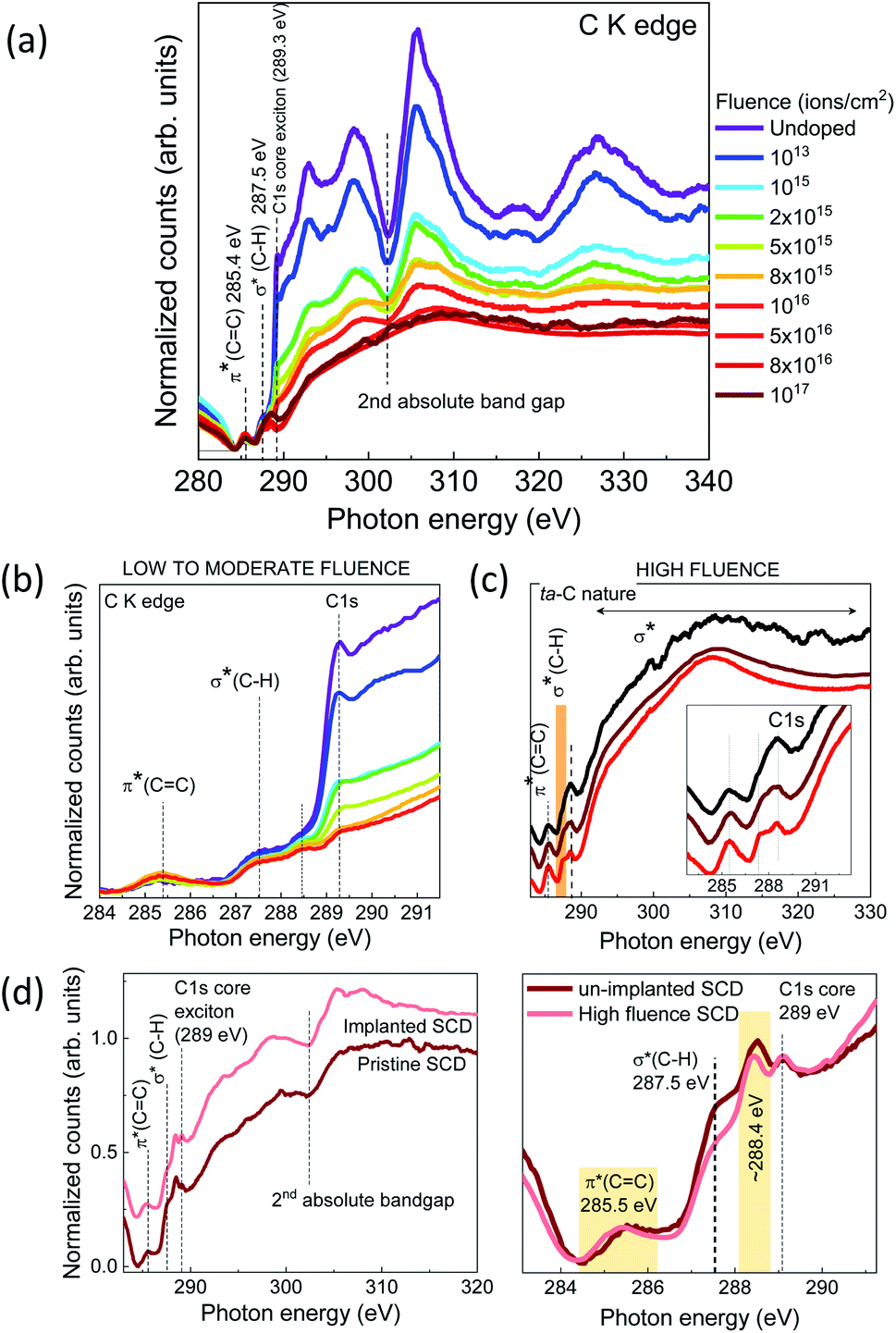 | ||
| Fig. 10 (a) C K edge XANES structure of implanted UNCDs at low, medium and high fluences, enlarged pre-edge XANES spectra for UNCDs implanted at (b) low and medium fluences and (c) high fluences; and (d) C K edge XANES structure for implanted and annealed SCD and compared with its pristine counterpart (left) and their corresponding pre-edge structure in the right panel. | ||
In the case of single crystal diamond (100), the long range order in implanted SCD remains unaffected except for those pre-edge resonance peaks as depicted in Fig. 10(d). No signature of crystalline graphite is found with implantations. Although the C 1s core excitonic peak seems unaffected by implantation, the sp2 π* absorption at 285.5 eV seems to increase while σ*(C–H) peak at 287.5 eV reduces in intensity which was evident in UNCDs as well due to reduction in sp3 hybridization; less sp3 means less surface dangling bonds and thus lesser hydrogen content at the surface of the sample. The broad peak at ∼288.4 eV is also of σ*(C–H) origin as already mentioned earlier. As this peak is also present in un-implanted SCD, we can not assign this to donor defect level created due to N-substitution below conduction band minimum. Therefore a reduced ratio of integrated peak area of σ*(C–H)/C 1s due to implantation symbolises a reduced sp3 content in implanted SCD samples. Although it is well established that implantation followed by thermal annealing at high temperatures >800 °C leads to graphitization of diamond,75,76 but we do not see a disordered structure due to complete graphitization at the diamond surface caused by implantation damages. Similar report on 500 eV neon-ion bombardment on diamond (100) surface showed that no phase transformation took place from defective implanted layers to graphite even after annealing.77 Since one can not deny the possibility of formation of graphitic clusters or a very thin graphitic layer upon annealing, we conclude that complete graphitization of the implanted layer in SCD does not happen even at this high fluence instead these are amorphous distorted sp3 rich clusters which also has sp2 bonding32,78 where percolation occurs to form a conductive pathway with semi-metallic like conductivity.
4. Summary and conclusion
We have been able to achieve highly conducting nitrogen implanted n-type polycrystalline (UNCD) as well as single crystal diamond (SCD) by proper choice of implantation and annealing conditions. The paper has been broadly classified into three parts where we try to explain our findings in three different ion dose regimes: low fluence region (<1015 cm−2; much lesser than the critical dose), medium fluence region (<1016 cm−2; still less than the amorphization limit, but sufficient to induce dense defects) and the high fluence region (where amorphization occurs). Ion implantation with low fluences introduce point defects which are recovered back easily by annealing. Moderate fluences introduce huge disorder into the system by forming large density of defects although the implanted lattice can still be restored back to its crystalline nature by annealing when the sp2 fraction is below 40%. High fluence implantation after annealing leads to the formation of tetrahedral amorphous carbon network (ta-C) where the sp3 fraction is still high but diamond looses its long range order as confirmed from X-ray absorption (XAS) results. XPS and SIMS results show the presence of deep implanted nitrogen layer in diamond films. We have tried to interpret the results from the perspective of sp2/sp3 ratio as we know that with implantation the sp2 content is bound to increase. After evaluating the sp2 fraction from XPS, it is clear that sp2% increases drastically in medium fluence regime and can rise up to 40% also confirmed by Raman data. In high fluence regime it becomes almost saturated at max. 50%. Similar results are seen in XANES data where as long as we are in low to moderate fluence regime, the sp2 fraction (evident from increase in π*(C![[double bond, length as m-dash]](https://www.rsc.org/images/entities/char_e001.gif) C) peak) increases systematically but as we go to high fluence implantations, the sp2/sp3 ratio no longer increases, instead it is almost same for all doses in that regime. Although the sp2/sp3 ratio remains constant, the diamond looses its long range ordering and becomes ta-C.
C) peak) increases systematically but as we go to high fluence implantations, the sp2/sp3 ratio no longer increases, instead it is almost same for all doses in that regime. Although the sp2/sp3 ratio remains constant, the diamond looses its long range ordering and becomes ta-C.
The low temperature electrical properties give proof of the fact that nitrogen incorporation brings enhanced conductivity of the order ∼650 Ω−1 cm−1. Insulator-to-metal transition (IMT) has been observed when implanted with more than 5 × 1016 cm−2 fluence where the nitrogen concentration is of the order of nN ∼ 1020 cm−3. UNCDs implanted with low fluences <1015 cm−2 (kFl ≪ 1) show hopping conductivity from 300 to 100 K following Mott's VRH model (Anderson–Mott insulator) whereas UNCDs implanted with high fluences (kFl > 1) follow the metallic conductivity given by quantum corrections to Boltzmann conductivity (QCC). Therefore, the metallic conductivity that we see in the high fluence regime is mainly due to the percolative conductivity because of sp3 bond breakage and not due to doping of the diamond nano-grains or doping of sp2 content in grain boundaries. We believe that in the low fluence region, the N-doping of the GBs start first because nitrogen is preferred more in the GBs and leads to the formation of defect band (by sp2 C π* density of states in the diamond bandgap) closer to the Fermi level where hopping conduction takes place. As the fluence increases and goes over to medium fluence regime, delocalization happens and the N-doping of the diamond nano-grains start too along with GB doping which brings in isolated N-donors into the system leading to substitutional doping forming N-donor level whose merger with the C π* states results in pushing the Fermi level further closer to the conduction band. Here the films are semiconducting in nature and the diamond long range order is still intact (evident in XAS) with a little compromise on the sp2 fraction. The Hall concentration too increases and these films show n-type behaviour. With fluence increasing, a sharp increase in electron concentration (ne) is also seen which when falls in high fluence regime decreases gradually. Actually when the fluence reaches a critical limit, the diamond transforms into a form of “highly disordered diamond” resembling a metallic glassy behaviour evident from its electrical transport behaviour. Although amorphization (i.e. sp3 bond breakage and distortion and loss of long-range order in diamond) occurs at high implantations, it does not lead to increase in diamond's conductivity rather conductivity decreases when it transforms into ta-C; quite opposite to what we expect normally.
Similar kind of studies have also been carried out in the case of single crystal (100) diamond. A reduction in the intensity of the diamond peak and also the appearance of a weak defect peak at ∼1600 cm−1 in Raman spectra is evident but there is no loss of long-range order in the system as observed in XAS results. XAS results also show that although a small increase in the sp2 content in the system is seen (evident from π*(CC) peak at 285.5 eV) but mostly it is the decrease in the σ*(C–H) at 288 eV peak due to desorption of surface hydrogen upon annealing in vacuum at high temperature. The overall electronic structure remains same if we compare implanted SCD with an un-implanted one. In single crystalline diamond, implantation leads to a scenario equivalent to creation of local defects or distorted amorphous regions which are still sp3 rich. While the temperature dependence of its resistivity resembles that of polycrystalline graphite (although absolute value of resistivity is far much higher than graphite in implanted SCD; ρgraphite < 10−6 Ω cm), the magnetoresistance behaviour follows that of metallic glasses.
A similarity between polycrystalline and single crystal diamond concludes that the electrical properties are not driven by just ‘GB transport mechanism’ rather it is the intrinsic property of diamond itself. Therefore, we find no conclusive evidence of substitutional doping of nitrogen in single crystal diamond however implantation with medium fluences in UNCD makes it n-type with electron mobilities μe ∼ 0.2 cm2 V−1 s−1 (much greater than mobility values reported in amorphous carbon phase in GBs) which gives clues about doping in diamond nano-grains as well along with GB doping. Achieving high conductivity in bulk diamond has been challenging, and thus, diamond films in ultra-nanocrystalline diamond (UNCD) form made up of small sp3 grains surrounded with an increased GB fraction when implanted with low to medium fluences can be easily made n-type which can promise efficient applications in high-temperature heterojunction electronic devices.
Conflicts of interest
There are no conflicts to declare.Acknowledgements
This work was supported by Department of Science and Technology (DST), New Delhi, that facilitated the establishment of “Nano Functional Materials Technology Centre” (Grant: SRNM/NAT/02-2005) and Physical Property Measurement System (PPMS) utilized for characterization is a DST-FIST Facility (SR/FST/PSII-038/2016) under the Department of Physics, IIT Madras. Authors would like to thank Dr K. Asokan and Dr D. M. Phase and acknowledge the LEIBF facility availed at IUAC, New Delhi, India where the ion implantation was carried out and the beamline facility (BL-1) availed at Indus-2 in RRCAT, Indore, India.References
- S. Koizumi, H. Umezawa, J. Pernot and M. Suzuki, Power Electronics Device Applications of Diamond Semiconductors, Woodhead publishing, 2018 Search PubMed.
- R. Farrer, Solid State Commun., 1969, 7, 685–688 CrossRef CAS.
- H. Sternschulte, K. Thonke, R. Sauer and S. Koizumi, Phys. Rev. B: Condens. Matter Mater. Phys., 1999, 59, 12924 CrossRef CAS.
- E. Gheeraert, N. Casanova, A. Tajani, A. Deneuville, E. Bustarret, J. Garrido, C. Nebel and M. Stutzmann, Diamond Relat. Mater., 2002, 11, 289–295 CrossRef CAS.
- J. Orwa, K. Nugent, D. Jamieson and S. Prawer, Phys. Rev. B: Condens. Matter Mater. Phys., 2000, 62, 5461 CrossRef CAS.
- R. Brunetto, G. Baratta and G. Strazzulla, J. Appl. Phys., 2004, 96, 380–386 CrossRef CAS.
- C. Uzan-Saguy, C. Cytermann, R. Brener, V. Richter, M. Shaanan and R. Kalish, Appl. Phys. Lett., 1995, 67, 1194–1196 CrossRef CAS.
- R. Kalish, A. Reznik, K. Nugent and S. Prawer, Nucl. Instrum. Methods Phys. Res., Sect. B, 1999, 148, 626–633 CrossRef CAS.
- D. Saada, J. Adler and R. Kalish, Int. J. Mod. Phys. C, 1998, 9, 61–69 CrossRef.
- S. Prawer and R. Kalish, Phys. Rev. B: Condens. Matter Mater. Phys., 1995, 51, 15711 CrossRef CAS.
- J. Nakata, Phys. Rev. B: Condens. Matter Mater. Phys., 1999, 60, 2747 CrossRef CAS.
- J. Hauser, J. Patel and J. Rodgers, Appl. Phys. Lett., 1977, 30, 129–130 CrossRef CAS.
- X. Hu, J. Ye, H. Liu, Y. Shen, X. Chen and H. Hu, J. Appl. Phys., 2011, 109, 053524 CrossRef.
- J. F. Prins, Phys. Rev. B: Condens. Matter Mater. Phys., 2000, 61, 7191 CrossRef CAS.
- X. Hu, J. Ye, H. Hu, X. Chen and Y. Shen, Appl. Phys. Lett., 2011, 99, 131902 CrossRef.
- S. Bhattacharyya, Phys. Rev. B: Condens. Matter Mater. Phys., 2004, 70, 125412 CrossRef.
- S. Bhattacharyya, O. Auciello, J. Birrell, J. Carlisle, L. Curtiss, A. Goyette, D. Gruen, A. Krauss, J. Schlueter and A. Sumant, et al., Appl. Phys. Lett., 2001, 79, 1441–1443 CrossRef CAS.
- T. Ikeda, K. Teii, C. Casiraghi, J. Robertson and A. Ferrari, J. Appl. Phys., 2008, 104, 073720 CrossRef.
- P. Achatz, O. A. Williams, P. Bruno, D. Gruen, J. Garrido and M. Stutzmann, Phys. Rev. B: Condens. Matter Mater. Phys., 2006, 74, 155429 CrossRef.
- P. Zapol, M. Sternberg, L. A. Curtiss, T. Frauenheim and D. M. Gruen, Phys. Rev. B: Condens. Matter Mater. Phys., 2001, 65, 045403 CrossRef.
- Y. Dai, D. Dai, C. Yan, B. Huang and S. Han, Phys. Rev. B: Condens. Matter Mater. Phys., 2005, 71, 075421 CrossRef.
- J. Ziegler, J. Biersack and U. Littmark, The Stopping and Ranges of Ions in Matter, 1985 Search PubMed.
- A. Ferrari and J. Robertson, Phys. Rev. B: Condens. Matter Mater. Phys., 2001, 63, 121405 CrossRef.
- A. C. Ferrari and J. Robertson, Philos. Trans. R. Soc., A, 2004, 362, 2477–2512 CrossRef CAS PubMed.
- D. S. Knight and W. B. White, J. Mater. Res., 1989, 4, 385–393 CrossRef CAS.
- R. Buckley, T. Moustakas, L. Ye and J. Varon, J. Appl. Phys., 1989, 66, 3595–3599 CrossRef CAS.
- J. Hunn, S. Withrow, C. White and D. Hembree, Jr, Phys. Rev. B: Condens. Matter Mater. Phys., 1995, 52, 8106 CrossRef CAS PubMed.
- E. Lee, D. Hembree, Jr, G. Rao and L. Mansur, Phys. Rev. B: Condens. Matter Mater. Phys., 1993, 48, 15540 CrossRef CAS PubMed.
- J. Wagner, M. Ramsteiner, C. Wild and P. Koidl, Phys. Rev. B: Condens. Matter Mater. Phys., 1989, 40, 1817 CrossRef CAS.
- A. Ferrari, S. Rodil and J. Robertson, Phys. Rev. B: Condens. Matter Mater. Phys., 2003, 67, 155306 CrossRef.
- A. C. Ferrari and J. Robertson, Phys. Rev. B: Condens. Matter Mater. Phys., 2000, 61, 14095 CrossRef CAS.
- A. Zaitsev, N. Kazuchits, V. Kazuchits, K. Moe, M. Rusetsky, O. Korolik, K. Kitajima, J. Butler and W. Wang, Diamond Relat. Mater., 2020, 107794 CrossRef CAS.
- H. graphite and hexagonal carbon, (PDF 898487, 897213, 65-6212) and (PDF 501084).
- A. Patterson, Phys. Rev., 1939, 56, 978 CrossRef CAS.
- N. Mott and J. Davies, Philos. Mag. B, 1980, 42, 845–858 CAS.
- P. A. Lee and T. Ramakrishnan, Rev. Mod. Phys., 1985, 57, 287 CrossRef CAS.
- N. Mott, Adv. Phys., 1967, 16, 49–144 CrossRef CAS.
- N. F. Mott and W. Twose, Adv. Phys., 1961, 10, 107–163 CrossRef CAS.
- M. Gurvitch, Phys. Rev. B: Condens. Matter Mater. Phys., 1981, 24, 7404 CrossRef CAS.
- A. Ioffe and A. Regel, Prog. Semicond., 1960, 4, 237–291 Search PubMed.
- L. Klibanov, M. Oksman, A. Seidman and N. Croitoru, Diamond Relat. Mater., 1997, 6, 1152–1156 CrossRef CAS.
- W. Mycielski, E. Staryga, A. Lipiński, S. Mitura and A. Sokołowska, Diamond Relat. Mater., 1994, 3, 858–860 CrossRef CAS.
- I. Beloborodov, P. Zapol, D. Gruen and L. Curtiss, Phys. Rev. B: Condens. Matter Mater. Phys., 2006, 74, 235434 CrossRef.
- M. Howson and D. Greig, J. Phys. F: Met. Phys., 1986, 16, 989 CrossRef CAS.
- S. Nagel, Phys. Rev. Lett., 1978, 41, 990 CrossRef CAS.
- S. Kajihara, A. Antonelli, J. Bernholc and R. Car, Phys. Rev. Lett., 1991, 66, 2010 CrossRef.
- W. Kaiser and W. Bond, Phys. Rev., 1959, 115, 857 CrossRef CAS.
- D. Das, A. Kandasami and M. Ramachandra Rao, Appl. Phys. Lett., 2021, 118, 102102 CrossRef CAS.
- C. A. Klein, Rev. Mod. Phys., 1962, 34, 56 CrossRef.
- M. Endo, Y. Hishiyama and T. Koyama, J. Phys. D: Appl. Phys., 1982, 15, 353 CrossRef CAS.
- L. Woolf, J. Chin, Y. Lin-Liu and H. Ikezi, Phys. Rev. B: Condens. Matter Mater. Phys., 1984, 30, 861 CrossRef CAS.
- T. Chieu, G. Timp, M. Dresselhaus, M. Endo and A. Moore, Phys. Rev. B: Condens. Matter Mater. Phys., 1983, 27, 3686 CrossRef CAS.
- Y. Koike, S. Morita, T. Nakanomyo and T. Fukase, J. Phys. Soc. Jpn., 1985, 54, 713–724 CrossRef CAS.
- B. Gallagher, D. Greig and M. Howson, J. Phys. F: Met. Phys., 1984, 14, L225 CrossRef CAS.
- R. Chambers, Proc. Phys. Soc., Sect. A, 1952, 65, 903 CrossRef.
- E. Sondheimer and A. H. Wilson, Proc. Roy. Soc. Lond. Math. Phys. Sci., 1947, 190, 435–455 Search PubMed.
- B. L. Altshuler and A. G. Aronov, Modern Problems in condensed matter sciences, Elsevier, 1985, vol. 10, pp. 1–153 Search PubMed.
- M. Howson and D. Greig, Phys. Rev. B: Condens. Matter Mater. Phys., 1984, 30, 4805 CrossRef CAS.
- T. Rosenbaum, R. Milligan, G. Thomas, P. Lee, T. Ramakrishnan, R. Bhatt, K. DeConde, H. Hess and T. Perry, Phys. Rev. Lett., 1981, 47, 1758 CrossRef CAS.
- B. AlTshuler and A. Aronov, Zh. Eksp. Teor. Fiz., 1979, 77, 2028–2044 CAS.
- B. Altshuler, D. KhmelNitzkii, A. Larkin and P. Lee, Phys. Rev. B: Condens. Matter Mater. Phys., 1980, 22, 5142 CrossRef CAS.
- Y. Toyozawa, J. Phys. Soc. Jpn., 1962, 17, 986–1004 CrossRef.
- R. Khosla and J. Fischer, Phys. Rev. B: Solid State, 1970, 2, 4084 CrossRef.
- W. Sasaki, J. Phys. Soc. Jpn., 1965, 20, 825–833 CrossRef CAS.
- V. Bayot, L. Piraux, J.-P. Michenaud and J.-P. Issi, Phys. Rev. B: Condens. Matter Mater. Phys., 1989, 40, 3514 CrossRef CAS PubMed.
- R. Khosla and J. Fischer, Phys. Rev. B: Solid State, 1972, 6, 4073 CrossRef CAS.
- H. P. Hjalmarson, H. Büttner and J. D. Dow, Phys. Rev. B: Condens. Matter Mater. Phys., 1981, 24, 6010 CrossRef CAS.
- J. Morar, F. Himpsel, G. Hollinger, G. Hughes and J. L. Jordan, Phys. Rev. Lett., 1985, 54, 1960 CrossRef CAS PubMed.
- K. A. Jackson and M. R. Pederson, Phys. Rev. Lett., 1991, 67, 2521 CrossRef CAS PubMed.
- J. Nithianandam, Phys. Rev. Lett., 1992, 69, 3108 CrossRef CAS PubMed.
- Z. Shpilman, I. Gouzman, T. Minton, L. Shen, A. Stacey, J. Orwa, S. Prawer, B. Cowie and A. Hoffman, Diamond Relat. Mater., 2014, 45, 20–27 CrossRef CAS.
- A. Hoffman, G. Comtet, L. Hellner, G. Dujardin and M. Petravic, Appl. Phys. Lett., 1998, 73, 1152–1154 CrossRef CAS.
- A. Laikhtman, I. Gouzman, A. Hoffman, G. Comtet, L. Hellner and G. Dujardin, J. Appl. Phys., 1999, 86, 4192–4198 CrossRef CAS.
- A. Gutiérrez, J. Diaz and M. F. López, Appl. Phys. A: Mater. Sci. Process., 1995, 61, 111–114 CrossRef.
- A. Gippius, R. Khmelnitsky, V. Dravin and A. Khomich, Diamond Relat. Mater., 2003, 12, 538–541 CrossRef CAS.
- J. Koike, D. Parkin and T. Mitchell, Appl. Phys. Lett., 1992, 60, 1450–1452 CrossRef CAS.
- L. Huang, I. Bello, W. Lau, S.-T. Lee, P. Stevens and B. DeVries, J. Appl. Phys., 1994, 76, 7483–7486 CrossRef CAS.
- B. A. Fairchild, S. Rubanov, D. W. Lau, M. Robinson, I. Suarez-Martinez, N. Marks, A. D. Greentree, D. McCulloch and S. Prawer, Adv. Mater., 2012, 24, 2024–2029 CrossRef CAS PubMed.
| This journal is © The Royal Society of Chemistry 2021 |