
 Open Access Article
 This Open Access Article is licensed under a Creative Commons Attribution-Non Commercial 3.0 Unported Licence
Reducing the resistance for the use of electrochemical impedance spectroscopy analysis in materials chemistry
Nadia O. Laschuk *,
E. Bradley Easton and
Olena V. Zenkina*
*,
E. Bradley Easton and
Olena V. Zenkina*
Ontario Tech University, 2000 Simcoe St N, Oshawa, ON L1G 0C5, Canada. E-mail: Nadia.Laschuk@ontariotechu.ca; Brad.Easton@onratiotechu.ca; Olena.Zenkina@ontariotechu.ca
First published on 18th August 2021
Abstract
Electrochemical impedance spectroscopy (EIS) is a highly applicable electrochemical, analytical, and non-invasive technique for materials characterization, which allows the user to evaluate the impact, efficiency, and magnitude of different components within an electrical circuit at a higher resolution than other common electrochemical techniques such as cyclic voltammetry (CV) or chronoamperometry. EIS can be used to study mechanisms of surface reactions, evaluate kinetics and mass transport, and study the level of corrosion on conductive materials, just to name a few. Therefore, this review demonstrates the scope of physical properties of the materials that can be studied using EIS, such as for characterization of supercapacitors, dye-sensitized solar cells (DSSCs), conductive coatings, sensors, self-assembled monolayers (SAMs), and other materials. This guide was created to support beginner and intermediate level researchers in EIS studies to inspire a wider application of this technique for materials characterization. In this work, we provide a summary of the essential background theory of EIS, including experimental design, signal responses, and instrumentation. Then, we discuss the main graphical representations for EIS data, including a scope of the foundation principles of Nyquist, Bode phase angle, Bode magnitude, capacitance and Randles plots, followed by detailed step-by-step explanations of the corresponding calculations that evolve from these graphs and direct examples from the literature highlighting practical applications of EIS for characterization of different types of materials. In addition, we discuss various applications of EIS technique for materials research.
Introduction
Materials science is a rapidly growing field greatly applicable in the areas of petrochemicals, nanotechnology, plastics and coatings, and energy storage and harvesting, just to name a few.1 Electrochemical impedance spectroscopy (EIS) is a rapid, highly effective and non-invasive analytical electrochemical technique widely applied for the analysis of conductive materials. EIS compares the input of sinusoidal potential, leading to current, with the output current and potential.2 As a result, EIS enables the evaluation of the impact, efficiency, and magnitude of different components within an electrical circuit, called the circuit elements. EIS offers higher resolution than other common electrochemical techniques such as cyclic voltammetry or chronoamperometry.3 For comprehensive electrochemical measurements, it is the prevailing technique capable of evaluating kinetics and mass transport behavior,4–7 determining diffusion coefficients7,8 and rate constants,9–11 characterizing corrosion processes,12,13 elucidating the mechanisms of the reactions occurring on the surface of the electrode,14 and providing the surface coverage,9,11 just to name several of the vast capabilities.Compared to other electrochemical techniques, EIS measurements effectively differentiate between resistance (R) and capacitance (C), and this allows for the separation of the diffusion processes from other physiochemical processes in the circuit. EIS allows unambiguously distinguish between resistance and capacitance since the resistance of the system is independent of the frequency (f) for the alternating current (AC), but capacitance is inversely dependent on it.8,15 This is hardly possible using other electrochemical techniques because they get combined signals of capacitance and resistance, and separation is extremely tedious.
While some electrochemical techniques like CV and chronoamperometry are routinely employed for the characterization of new materials, utilizing EIS for materials characterization is still less common in the literature. Even when EIS data is reported, in-depth analysis of the data is often missing, and the full utility of the technique is overlooked. Thus, this review is aimed to serve as an all-in-one guide for materials science researchers and electrochemists to introduce the EIS technique to new users and provide advanced knowledge on this method of analysis. While some very interesting specialized reviews are reporting on practical applications of EIS for bioanalytical applications,16 to understand structure/performance relationships of metal oxides,15 and porous electrodes,8 the main goal of this manuscript is to bridge the gap that currently exists through a clear explanation of key terms and analysis, which are commonly not defined/explained within research manuscripts. Here, we review EIS techniques and highlight numerous practical applications within materials science, such as for analysis of self-assembled monolayers (SAMs),9,17,18 supercapacitors,19–22 dye-sensitized solar cells (DSSCs),23,24 conductive coatings,25–27 sensors,28,29 porous electrodes for different applications,30–32 and other “smart” materials.7,33,34 Very recent exciting literature examples that applied EIS to characterize, optimize or fully understand the performance of the material include analysis of on-skin or wearable sensors,35,36 “green” microbial fuel cells,37 and biosensors of SARS-CoV-2 antibodies.38,39 Notably, there are different methods to illustrate and analyze EIS measurements. The two most common graphical methods: Nyquist plots and Bode plots, are hereby described, and are compared to other procedures of the EIS analysis.
Introductory theory
Impedance
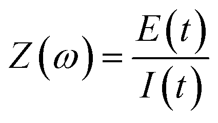
Impedance (Z, reported in Ω using SI units) refers to the amount of the opposition to current (I) flow that takes place under applied voltage within an electrical circuit. For the faradaic heterogeneous reaction where the charge transfer takes place at the surface of the electrode, the change in the impedance is a result of the adsorption of reacting species, diffusion of ions, and charge transfer by the redox species. It is impacted by the nature of the electrode-solution interface, electrolyte, morphology, and composition of the electrode materials.14EIS circuit responses
The EIS responses arise from the AC in a circuit while controlling the frequency (f) in Hz over the AC perturbation. The most common measurements record the current response by altering the frequency of a sinusoidal voltage (E) perturbation superimposed over a selected direct current (DC) voltage, called the applied bias (Eapp). The relationship in eqn (1) follows Ohm's law (V = IR) where ω is the angular frequency (s−1) calculated ω = 2πf.
 | (1) |
To get the most reliable results, the applied frequency should cover a large range, such as from 1 mHz to 100 kHz. This will induce a change to the observed amplitude abiding by the relationship described in eqn (2) where |E0| is an amplitude that Eapp is controlled over (e.g. ∼5–10 mV).15
E(t) = Eapp + |E0|![[thin space (1/6-em)]](https://www.rsc.org/images/entities/char_2009.gif) sin(ωt) sin(ωt)
| (2) |
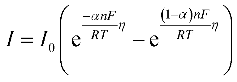
Eqn (2) gives the response of E(t) that is linearly dependent on I(t). It follows the Butler–Volmer model (eqn (3)) where I0 is the exchange current, α is the transfer coefficient for electron exchange, η is the overpotential from the equilibrium potential (E − Eq), n is the number of electrons transferred, T is the temperature in Kelvin, F is the Faraday constant, and R is the gas constant.40
 | (3) |
The current response correlates to the frequency, but experiences a phase shift with a magnitude that depends on the specific circuit's elements, where a phase shift is a horizontal translation on a sinusoidal axis. The size of this shift gives the phase angle (φ) following eqn (4).
|
I(t) = |I0|sin(ωt + φ)
| (4) |
The process will repeat over the frequency range for different applied biases. The length of the measurement will depend on the frequency range, and Eapp step size.15 The relationship between E(t) and I(t) is graphically presented in Fig. 1. Here, Fig. 1A shows the vertical translation of the E(t)'s sinusoidal curve caused by the application of Eapp. The I(t) does not experience this vertical translation, but its position is translated horizontally by φ. Thus, the wave for I(t) trails behind E(t), which is drawn on the same axis of rotation for clarity (i.e. E(t) − Eapp) in Fig. 1B.
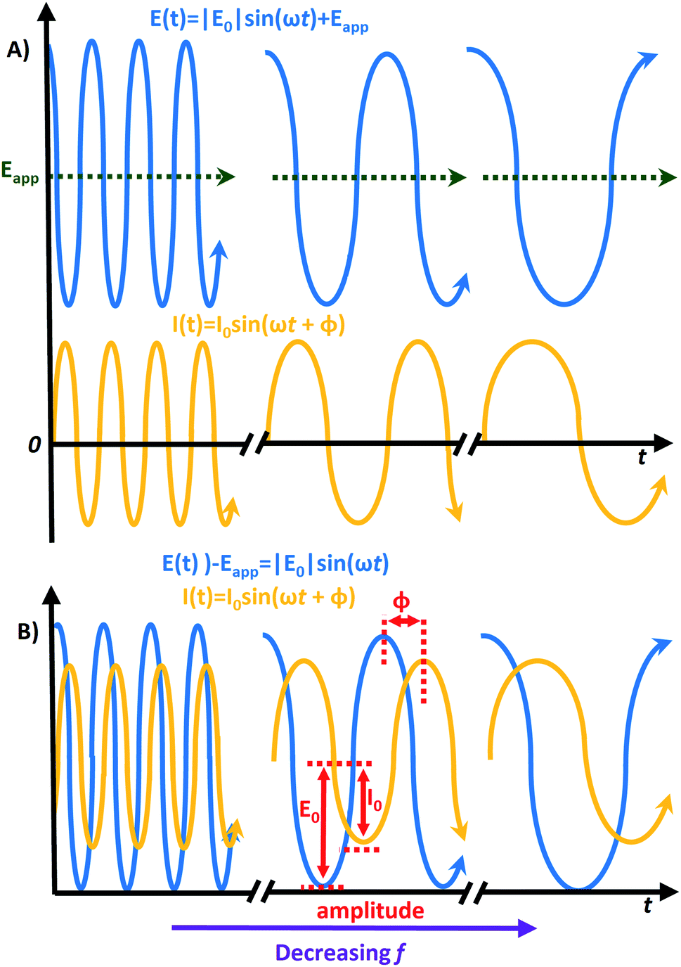 | ||
| Fig. 1 (A) Graphical representation of the equations E(t) = |E0|sin(ωt) + Eapp and I(t) = I0sin(ωt + φ), depicting their time dependence. (B) E(t) graphically presented on the same axis of rotation as I(t) to make visible the phase angle (φ)'s impact on the time-scale position of I(t) compared to E(t). | ||
Circuit elements
The physical processes involved in the electrochemical reaction can be represented by typical AC circuit elements. The presence and magnitude of each circuit element provide specific information about the physicochemical behaviour of the circuit. The most frequently encountered circuit elements of an AC circuit are the resistors and capacitors, where a circuit can include any number of these.40 There are different types of resistance, however, the four most prevalent are the ionic resistance (Rion), electronic resistance (Relec), bulk electrolyte (solution) resistance (RS), and charge transfer resistance (RCT). Rion and Relec account for the opposition to ionic and electronic movement within the structure of the electrode, respectively. RS is the resistance between the working electrode (WE) and reference (RE) (note: in a 2-electrode cell, the counter electrode (CE) serves as the RE).17 RCT is the electron transfer resistance across the electrode–electrolyte interface.11 Furthermore, the double-layer capacitance (Cdl) gives the specific capacitance at the interface of the electrolyte with the electrode, and is characterized by the non-faradaic charge that arises from the surface, either from the solid/solid, solid/liquid, or liquid/liquid interface (depending on the nature of your electrode). Inductors (L) are less commonly encountered in EIS circuits, however, they may be required to fully describe the circuit. Inductance occurs as a result of close contact of metal surfaces, such as between metallic materials or leads, and has the opposite relationship to frequency compared to the capacitance.15,40AC circuits are represented by circuit models, which are diagrams that highlight the components of the individual circuits. For example, the behavior of the very simple AC circuit with no faradaic process represented on Fig. 2A is close to the behavior of an ideal circuit. Conversely, Fig. 2B represents a circuit for a system with a faradaic process.2 A faradaic process is charge transfer across an interface due to redox reactions, where the transferred electrons can be injected or be withdrawn from the electrodes.41
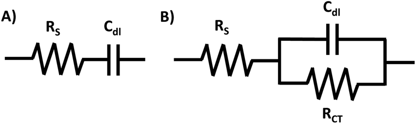 | ||
| Fig. 2 Sample simple circuits: (A) without faradaic process and (B) with a faradaic process. | ||
Performing measurements
To measure EIS, a standard electrochemical cell device design can be applied, as commonly used for many electrochemical experiments. For example, a 3-electrode cell device requires the sample in a cell with electrolyte, a WE, CE and RE.42 A schematic set-up and detailed procedures for performing a 3-electrode cell electrochemical measurement are elsewhere reviewed.43 Classically, measurements are recorded by pairing a potentiostat to an impedance/gain-phase analyzer, (for example a Solartron 1250/1255/1260 series frequency response analyzer). The function of an impedance/gain-phase analyzer is to record a sinusoidal response of the impedance of a circuit as a function of time at the wide range of changing frequencies. The researcher can make a number of customizations, such as choosing the initial and final frequency values, the interval frequency value, and the number of points recorded. The equipment is able to record the phase shift that takes place between the input and output signals, and then after each frequency step. Methodology varies between instruments, but an example pathway for a signal would proceed as follows: the impedance/gain-phase analyzer has a sinusoidal generator that creates frequency sweeps, a peak detector measures the amplitude of the signal, and a phase detector measures the phase shift between two signals. The instrumental design requires the computer to communicate to the instrument through a microcontroller. The instrument will pass a sinusoidal signal through the sample cell, and the outcome is measured. In operation, the researcher instructs the program to perform a frequency sweep and a digital-to-analog converter changes this input into a voltage value, which in turn controls the output frequency of the sinusoidal signal. This signal is maintained until a designated steady-state value is reached. Once at steady-state, a voltage reading of the peak detector and the phase detector is sent to the computer through an analog-to-digital conversion. This cycle continues until the sweep ends, either by the program or the operator.44Notably, newer instruments are now accessible which integrate digital signal processors into one potentiostat component, and do so at a greatly reduced cost, making impedance an accessible technique. For example, the BioLogic© Impedance analyzer has the capability to measure the impedance in one integrated device. This is different to the previous technologies, which required the analyzer to be coupled with a potentiostat for operation.
Modelling of EIS data
It is common for researchers who are new to EIS studies to face difficulties with data analysis and correlated calculations, which are comparatively more difficult and time-consuming than actual experimental set-up and measurements. To overcome the difficulties, a discussion on modeling and different graphical representations and analysis of EIS data is hereby discussed.To start the analysis of the EIS measurement, the data should be opened in the specialized software† and fitted to a suitable equivalent circuit model where the goal of curve fitting is to get the best correlation between experimental data points and the modelled curve, and the accuracy of the fit can be evaluated using chi-squares or the error distribution versus frequency.45 To do this, a circuit model has to be composed using circuit elements in a sequence that describes the AC circuit (examples of simple circuits with or without the faradaic process within the system are shown in Fig. 2). Equivalent circuits abide by Kirchoff's laws that permit the determination of the magnitude of individual components within a circuit. Due to the complexity of the functions, utilization of the specialized software designed for EIS data analysis is recommended.15 The correlation between the used circuit model and the EIS data was previously discussed elsewhere.46
The “Randles equivalent circuit model” is a model commonly applied to many conductive surfaces (Fig. 3). From the Randles circuit fit, the magnitude of the previously introduced circuit elements can be extracted: RS, RCT, Cdl. Additionally, there is the Warburg impedance (ZW) which is also called the impedance of diffusion or mass-transfer term and is a parameter that becomes significant in magnitude when a diffusion-controlled electron transfer process is present.47 In the Randles circuit, Cdl is sometimes substituted with a constant-phase element (Q), abbreviated CPE, to compensate for non-ideal capacitor behaviour that occurs due to non-homogeneity of the surface at the double-layer interface.9,18,45,48,49 The CPE is impacted by surface roughness, chemical inhomogeneity, and a heterogeneous electrode–electrolyte interface caused by ion adsorption.50
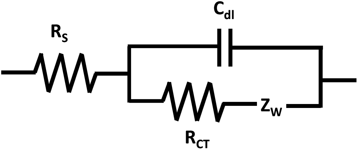 | ||
| Fig. 3 Randles equivalent circuit model. | ||
The magnitude of the circuit elements can provide unique information about the conductive material under investigation, such as estimate the effectiveness of electrode material enhancements,21,22,51 indicate the presence and magnitude of the corrosion processes,26,52,53 or evaluate the suitability of the experimental operating conditions and design.28 For example, EIS data was recently used to probe the extent of the degradation of electrochromic devices created with different CEs. In a 2-electrode cell set-up, there is no external RE (but the CE can serve as a pseudo-reference for some materials), and therefore the stability of the CE is critical to minimize potential drifts across the device and reduce polarization of the CE. In this work, the impedance of the device was measured before and after 3000 cycles of durability testing. The Randles circuit model was applicable for the device created with a non-porous CE. Thus, the magnitude of RCT was extracted before and after the long-term cycling to probe specific information about the influence of the nature of the CE on the rate of device degradation.52 Notably, EIS allowed early in situ monitoring of the degradation processes within the system.
While the Randles circuit diagram is commonly used, the applied equivalent circuit model largely depends on the nature of the conductive material. Proper representation of many electrochemical systems often requires more detailed diagrams than the Randles circuit to obtain a reasonable fit.12,17,45 In addition, the selected elements of the circuit model should represent meaningful parameters and processes of the system under investigation. A circuit model could provide a mathematically accurate fit (as evaluated by chi-squares or the error distribution versus frequency), but the results will not be valid if the circuit elements of the model do not provide a realistic physical representation of the sample.15 The software for viewing and modelling of the impedance data is able to present the data in both Nyquist and Bode plot format (vide infra).
Furthermore, one equivalent circuit may not be encompassing for EIS measurements of the same material under different conditions. For example, Sampath et al. used EIS to study the suitability of NiPS3 nanosheets for humidity sensing. When the measurements were recorded below 45% of relative humidity, the EIS data could be fitted to a simple equivalent circuit composed of a resistor (RCT) and CPE elements connected in parallel. However, above the threshold of 45% relative humidity, an additional CPE had to be added to the circuit model to compensate for the substantial change of the conductivity of the sensor with increasing relative humidity.28 Therefore the suitability of the circuit model depends not only on the nature of the system but also on the physical and chemical conditions of the measurements. For EIS analysis of thick and porous electrodes, the transmission-line model (TLM) (Fig. 4) sometimes appears as the best equivalent circuit model, and is often applied for supercapacitors, fuel cells, lithium ion batteries,54 and conducting polymers.55 For example, in the previously mentioned example, Ahmad et al. demonstrated that to describe the electrochromic device with the non-porous CE, the Randles circuit model showed the best fit (based on the shape of the Nyquist plot), while the TLM was required represent the same material in the device with porous CE.52
 | ||
| Fig. 4 Transmission line model (TLM) of a porous working electrode. | ||
Graphical analysis of EIS data
Nyquist plots
The “Nyquist plot” (also named as complex plane plot or Argand diagram) is most frequently applied in the literature, often due to its simplicity and best visibility. From the appearance of the Nyquist plot, one could estimate the nature and stability of the system without any additional calculations. A Nyquist plot is constructed by plotting the real part of impedance (Z′ or ZRe) on the x-axis and the negative value of the imaginary part of impedance (Z′′ or ZIm) on the y-axis, where the negative sign is required to keep the graph in the first quadrant of the Cartesian plane. This abides by the relationship described in eqn (5) where |Z| = (Z′2 + Z′′2)1/2 and φ = tan−1 (Z′′/Z′).3,15,40|
Z(ω) = |Z|(cos(φ) − jsin(φ)) = Z′ − jZ′′
| (5) |
As illustrated in Fig. 5A, the Z′ axis has an inverse relationship to the frequency, meaning that high applied frequency values appear on the left of the diagram and they decrease moving right along the x-axis. Each data point in the Nyquist diagram represents a different frequency value.15 The Z′ and Z′′ axis may be standardized by multiplying on the geometric surface area of the working electrode, yielding area-specific resistance and impedance values (e.g. with units of Ω cm2).3,56–58 This enables direct comparison of the EIS response of electrodes with different areas.
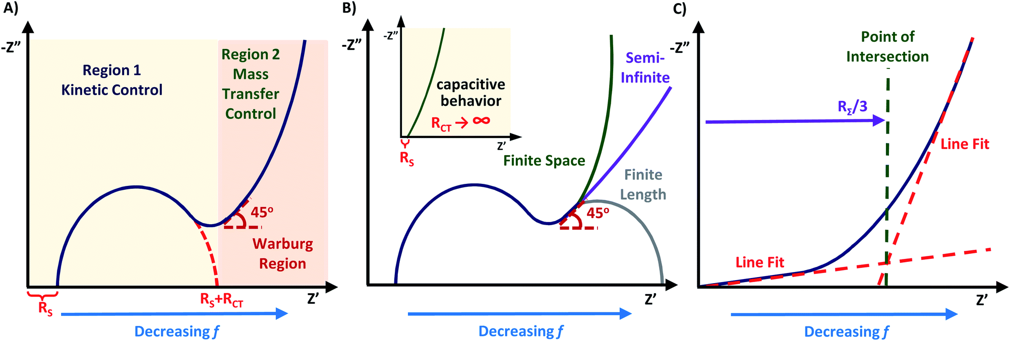 | ||
| Fig. 5 (A) Nyquist plot with key regions labelled. (B) Expansion of Nyquist plot region 2 with typical observed Warburg impedances occurring for different types of electrode materials. Inset of (B) shows how Nyquist plot would appear when displaying capacitive behaviour. (C) Calculation of RΣ using a linear line fit of the Warburg region. | ||
The Nyquist plot begins with the area of limited diffusion due to the high applied frequencies, and as a result, only charge transfer processes remain.59 Here, the x-intercept is equal to the magnitude of RS, and is viewed as a horizontal translation along the Z′ axis on the Nyquist plot.60 From this position, a semicircle region begins, which is an effect of the current passing through both Cdl and RCT. For materials with kinetically fast charge transfer, the diameter of the semicircle is very small (and vice versa). RCT can be extracted as the diameter of the first semicircle within the Nyquist plot. The magnitude of this parameter is obtained from the equivalent circuit model.61,62 In the mid-frequency region where maximum Z′′ is observed, the frequency (fmax) gives the time constant (τrxn) of the electrochemical reaction using eqn (6), and this constant is an indicator of how fast the electron transfer process is.3,40,59
 | (6) |
While one semicircle is most commonly observed, two or three semicircles are possible at lower frequencies, which represents multiple independent components that contribute to the overall impedance of the material.5,63 For example, a second arc at lower frequency region can take place from adsorption and desorption processes of ions at the electrode–electrolyte interface.14
As the frequency decreases, there is a second region where diffusion of charge at the electrode–electrolyte interface begins to thrive,19,59 and mass transfer of the redox species to and from the interfacial region becomes substantial.3 The Nyquist plot will display a characteristic oblique line with a 45° angle beyond the arc from region 1 known as the “Warburg region”. The frequency range of the Warburg region depends on the material being analyzed, such as occurring at high frequencies for fuel cells demonstrating no charge transfer arc,58,64 but happening at low frequencies for conductive supports with a charge transfer region.4–6 For the Warburg region, derivations from this ideal case of 45° are possible including variations to the angle (35°–55°) and nonlinearity, which can be a result of non-ideal behavior within the system.5,8 When the Warburg region continues to extend as a 45° linear line, it is called “semi-infinite Warburg impedance”. However, Nyquist plots can also depict “finite space Warburg impedance” and “finite-length Warburg impedance” (Fig. 5B). The finite space Warburg runs parallel to the Z′′ axis, and is defined as pure capacitance. Contrary to this, the finite length Warburg becomes purely resistive. These different characteristic features of Nyquist plots define the applied equivalent circuit model,4 and the positioning of the Warburg region on the plot. For the best visualization, it is wise to design the Nyquist plot in 1:1 aspect ratio for the x- and y-axis, to retain the semicircular shape of the charge transfer resistance arc and the 45° character of the Warburg region.14,17,45,65
Nyquist plots are often applied to study the performance of the electrochemical sensors and biosensors. This is typically done by monitoring the dependence of RCT of the system on the analyte concentration, conditions of the experiment or the architecture of the sensor. For example, the work of Ortiz-Aguayo et al. utilized the Nyquist plot to create a sensor demonstrating high affinity and specificity for the lysosome (Lys) protein. For this, changes of RCT values were monitored for different architectures of the sensing electrodes: the electrode capable of only protein blocking with polyethylene glycol (PEG) and the system that was additionally incubated with Lys protein. The Lys-exposed sample demonstrated higher values of RCT compared to RCT for the electrode that had only been subjected to blocking, and this knowledge was used to further optimize the incubations times for different components of the sensing electrode and to find the best-optimized electrode design.66
Application of the Nyquist model for characterization of self-assembled monolayers on the electrode surfaces
Interestingly, EIS has been applied for the characterization of conductive surfaces modified by insulating or redox-active self-assembled monolayers (SAMs) having a redox probe in solution (e.g. Fe(CN)63−). As shown in Fig. 6, the number of electrons transferred at the surface of the electrode declines with the increase of SAM surface coverage. As a result, the charge transfer arc (which provides the magnitude of RCT) increases, as shown in the correlated Nyquist diagrams. For an insulating SAM, RCT is expected to increase with the denser packing of the SAM. Thus, in this type of system, is always larger than RCT where RCT represents the unmodified surface and
  is the modified surface of the electrode. Because of the relationship between the resistance and the self-assembly, the fractional surface coverage (θimp) has been determined through eqn (7).
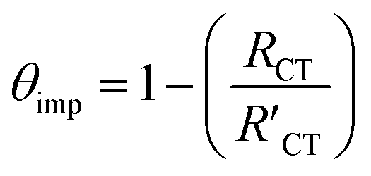 | (7) |
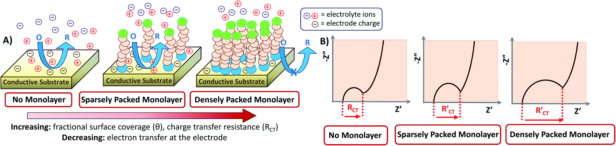 | ||
| Fig. 6 Diagram of the partial charge blocking across a SAM on a conductive substrate where (A) demonstrates the SAM layer formation with increasing surface coverage, and (B) gives the correlated Nyquist diagram. | ||
Eqn (7) has previously been applied for both redox-active and insulating monolayers.3,11,67 Furthermore, the same parameter can be determined using the peak current within CV (θCV).3,11,67 The comparability of θimp and θCV depends on the nature of the SAM. For example, insulating SAMs showed a higher value of θ with EIS because the CV value was unfavorably impacted by diffusion near the bare parts of the SAM-modified electrode.3,11 On the contrary, a redox-active SAM on the electrode results in higher values of surface coverage from EIS when compared to CV.17,67 However, the EIS-based calculations provide the best precision of the surface coverage calculation because this method separates the resistive and capacitive contributions.3,17
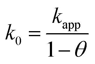
Because the insulating monolayer partially hinders electron transfer on the surface, the value of the actual electron transfer rate constant of the system becomes smaller than the value of the initially measured constant for the system with no coverage. The initial rate constant is called the “apparent electron transfer constant” (kapp), and is the measure of the kinetics for the electron transfer through the interface. Thereby, it is a heterogeneous rate constant. It is calculated from RCT using eqn (8) where A is the electrode area, C* is the concentration of the electrolyte (mol cm−3), n is the number of electrons transferred, T is the temperature in Kelvin, and F and R are the Faraday and gas constant, respectively.3,10
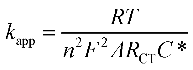 | (8) |
The equation applies for a one-electron first-order reaction. The real rate constant (k0) may then be determined using eqn (9).9
 | (9) |
This model has previously been used to evaluate SAMs deposited on gold substrates,9 and indium tin oxide (ITO) coated glass substrates.11
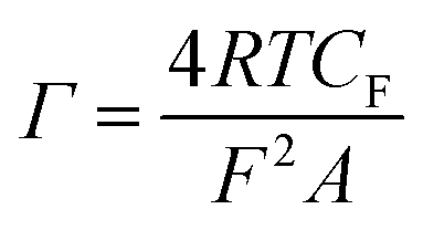
The redox-active SAM adds the faradaic capacitance (CF) (described below in ‘Capacitance plots’) component into the system. Here, eqn (10) can be applied to determine the surface packing (Γ) of the redox species in mol cm−2 on the substrate (R is the gas constant).17
 | (10) |
Internal resistance measurements
Systems that demonstrate “capacitive behavior” normally feature no noticeable semicircle on the Nyquist plot (RCT = infinite), and a nearly parallel increase of the impedance to the Z′′ axis (Fig. 5B inset).20 This is a common case for supercapacitors, batteries, and porous electrodes.7,68 The more vertical the line is to the Z′′ axis, the more closely the material behaves like an ideal capacitor.69 The changes to the internal resistance (RΣ) can be monitored through graphical analysis of the Warburg region. While factors that contribute to the internal resistance could be different for various types of conductive electrodes, the internal resistance generally represents the resistance that limits movement of electrons and ions within the system and therefore is described by the sum of Relec and Rion following eqn (11).70| RΣ = Rion + Relec | (11) |
To obtain RΣ, the real component of the Warburg is projected on to the Z′ axis (Fig. 5C). The projection is equal to RΣ/3, which can be rearranged to obtain the value of RΣ.57,58,71 For conductive materials, such as conducting polymers64 and fuel cells,57,58,71 Relec is insignificant and thus the value of RΣ is equal to Rion. Measurements of RΣ are useful to monitor how the internal resistance changes over time with durability cycling.57,65,71
For example, very recently EIS measurements were used to evaluate the durability of a porous sulfonated silica ceramic carbon electrode compared to the leading commercial Nafion™ based electrode. The materials were separately deposited on the platinum on carbon support to act as the electrode for a fuel cell, and were subjected to an accelerated stress test (following a protocol recommended by the US Department of Energy) which included measurement of cyclic voltammograms (CVs) for 10000 cycles with periodic measurement of the impedance within the double layer at the potential region for the same bias potential each time. The change in magnitude of RΣ over the cycles was displayed graphically following calculations of RΣ for the EIS measurements. The authors observed a substantial incrementation to the magnitude of RΣ over the stress test for the leading Nafion™ based electrode, confirming the occurrence of detrimental carbon corrosion. However, only a slight increase in RΣ was reported for the sulfonated silica ceramic carbon electrode owing to its drastically improved stability.68
Capacitance plot
If the conductive material demonstrates efficient mass transport such as through a finite space Warburg or semi-infinite Warburg impedance in the low-frequency region on the Nyquist plot, then the diffusion coefficient can be calculated using a Randles plot. Additionally, the capacitance of the material can be evaluated through the capacitance plot.As previously introduced, capacitive behavior is characterized by prominent ion diffusion within the system, and is observed in the Nyquist plot through finite space Warburg impedance.19 The capacitance, formally called the series capacitance (SI unit F) can be calculated using eqn (12) and is inversely dependent on the angular frequency.
 | (12) |
Capacitance can be further scrutinized through a capacitance plot, which is constructed as C versus Z′ (Fig. 7A). The capacitance plot could also be composed with frequency on the x-axis in place of Z′,56 thus vertically reflected with respect to Fig. 7A and obtaining the capacitance value on the left-hand side. Capacitance plots allow for obvious indication of the amount of ionic resistivity within a material.57
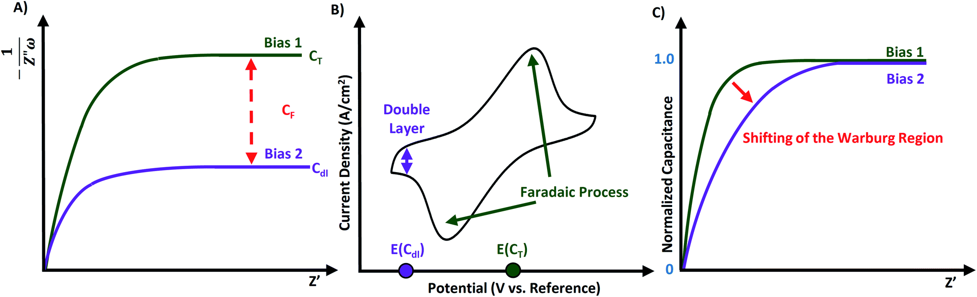 | ||
| Fig. 7 (A) Capacitance plot featuring two separate impedance measurements where bias 1 corresponds to a measurement with a faradic response, and bias 2 represents a measurement with no faradaic response in the double layer. (B) Sample cyclic voltammogram from which the bias potentials of Cdl and CT can be determined. (C) Normalized capacitance plot demonstrating how the capacitance measurements from (A) would appear if normalized to their maximum value. | ||
Faradaic capacitance (or pseudocapacitance) is electrochemical storage as a result of faradic reactions within the material/capacitor. For reactions that are not limited by diffusion and feature rapid electron transfer processes, the value of RCT approaches a limit (as was depicted in Fig. 5B inset). Thus, the capacitive contribution to the impedance could be solely attributed to the faradaic reactions in the system. If faradaic processes occur on the surface or near the surface of the material, then its CF value can be obtained from the capacitance plot following eqn (13) where CT is the maximum (“total”) observed capacitance at low frequencies, and Cdl is the limiting capacitance of the double layer.
| CT = Cdl + CF | (13) |
Impedance spectra should be reported at the bias potential in the double-layer region, and at bias potentials corresponding to each faradaic process. Measuring CVs is the simplest way to determine these specific bias potentials. As seen in Fig. 7B, the CV shows all faradaic processes, while the double layer is in the baseline. If no faradaic processes are present within the material, then eqn (13) reduces to CT = Cdl.58 Another method is to determine the magnitude for Cdl by measuring the sample without the faradaic species on the material (e.g. a highly porous carbon), and to assume that this Cdl value will remain unchanged when the faradaic process is present (e.g. the same carbon now doped with redox species).3
Cdl is an important feature of electrochemical materials. This parameter is often related to key electrocatalytic properties of the materials since Cdl is directly related to the surface area. For example, recent work of Fruehwald et al. reported on the mesoporous nickel on graphene oxide-based electrocatalyst for the oxygen reduction reaction (OER) that demonstrated an impressive OER performance. Notably, this high-performing catalyst was featuring a significantly higher Cdl than majority of typical nickel on carbon catalytic systems.72
A variation of the capacitance plot is the “normalized capacitance plot”, where the quotient of C to the maximum capacitance (i.e. y = C/Cmax) versus capacitance is plotted for each individual bias measurement. Fig. 7C shows how the EIS data from Fig. 7A would be transformed into a normalized depiction. Using normalized capacitance plots, one can readily visualize differences in RΣ for electrodes with vastly different capacitances. This feature is particularly advantageous for performing durability cycling, where both parameters (i.e. C and RΣ) can vary significantly from the beginning and end of the test.57,58
The method of capacitance and normalized capacitance plots was previously used to reveal the pseudocapacitance of electrochromic energy storage devices. An electrochromic working electrode (ECWE) was prepared using a mixture of chromophoric iron(II), osmium(II) and cobalt(II) metal complexes with 4′-(pyridin-4-yl)-2,2′:6′,2′′-terpyridine (L) ([Fe(L)2]2+, [Os(L)2]2+, [Co(L)2]2+) on conductive and porous surface-enhanced ITO supports. Each type of embedded complex was bearing unique faradaic redox process. As a result, three different faradaic processes occurred within the same system at different potentials (E1/2), as revealed through CV for the redox couples of Fe2+/3+, Os2+/3+, and Co2+/3+. The Nyquist plot for the ECWE did not demonstrate distinct differences between the applied biases even with a region expansion to enhance the visibility of Warburg region. However, the data presented in a capacitance plot format allowed for the effective separation of the capacitance at the applied bias for each distinct redox process. Furthermore, converting this data into a normalized capacitance plot revealed the shifting of the Warburg region (e.g. see Fig. 7C) for the more resistive redox processes within the same ECWE. This allowed for clear indication of the most conductive components of the ECWE.73
Randles plot
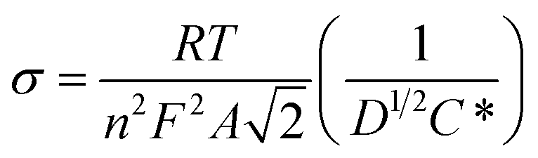
A Randles plot is composed of Z′ versus the negative root of the angular frequency (ω−1/2). The low-frequency region has a nearly linear section where the slope is equal to Warburg coefficient (σ) in Ω s−1/2 as demonstrated in Fig. 8.3,19 The Warburg coefficient is then used to obtain the diffusion coefficient (D) in cm2 s−1 using eqn (14) (R is the gas constant and other constants were previously defined).
 | (14) |
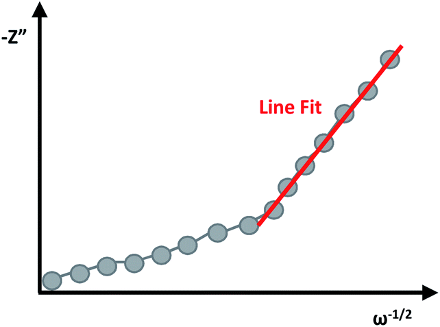 | ||
| Fig. 8 Example of a Randles plot with the line fitting in the low-frequency region. | ||
The diffusion coefficient, also called the mass-transfer parameter, is a measure of the amount of molar flux to pass through a surface. This follows Fick's second law of diffusion, thus larger values of the diffusion coefficient represent faster ion movement.3,5,19 The limitation to the equation is that the condition κl ≫ 1 must be satisfied where κ = (ω/2D)1/2 and l is the film thickness. The linear region of the low-frequency range will depend on the specific material, and eqn (14) will be satisfied when the slopes of Z′ versus ω−1/2 and Z′′ versus ω−1/2 are approximately equal.25
This method for the determination of diffusion coefficients has been effectively applied to describe and compare the performance of different supercapacitors.7,19,74 Particularly, this method was used to study the suitability of different geometric architectures of porous copper(II) oxide nanostructures for supercapacitor application. In this work, pseudocapacitive three-dimensional architectures (3D) of CuO electrodes were prepared through the organized assembly of one-dimensional (1D) and two-dimensional (2D) nanostructures. The EIS analysis was used to differentiate between two different 3D architectures named the “nanourchins” and “nanoflowers”, and to study their performance as supercapacitors in comparison to the foundational material, the 2D nanoflakes. The measurements were fitted to the Randles circuit model. Notably, 3D architectures demonstrated the value of D to be three times greater compared to the 2D foundation architecture, and the “nanoflower” 3D assembly experienced slightly better diffusion than the “nanourchin” architecture owing to the advantageous structural design.19
Bode plots
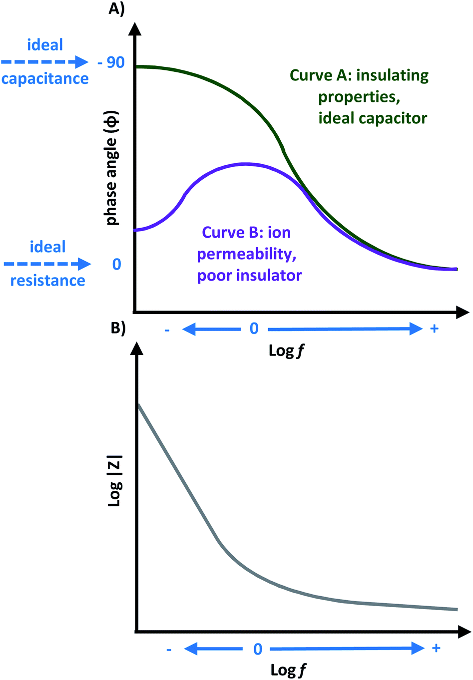
Bode plots are the second main format of EIS graphical representation. These are less popular than Nyquist plots, yet contain a key information corresponding to the applied frequency such as increased sensitivity to changes in capacitance, resistance, and ion diffusion.14,75 Bode plots come in two forms. For both types of Bode plots, the log of the frequency is plotted on the x-axis. Then, the y-axis will host either the measured phase angle (φ) or log|Z|. These are called the “Bode phase angle plot” and “Bode magnitude plot”, respectively. It is noted that some authors use modified versions of the Bode plot where the measured frequency is used instead of its logarithm.14,20,23,24,67
Capacitors are often studied using Bode phase angle plots. The phase angle at low frequencies gives specific information about the electrode. An ideal capacitor is expected to have an observed angle of −90°, which is ideal for insulating electrodes,20,45,76 because the −90° phase angle represents the maximum possible phase shift between the voltage and current. Thus, significant decreases from this value represent the dielectric layer being less able to effectively hold an electric charge, and reveal electron flow. This would be a result of the current leakage at defect sites or pinholes in the heterogeneous dielectric layer, causing a decline in the total impedance.48,76 A phase angle near −45° is indicative for pseudocapacitance.20 As an example, in Fig. 9A, two commonly observed response curves for Bode phase angle plots are presented (not limited to only these curves shapes). For curve A, a higher phase angle is observed at low frequencies which suggests lower ionic permeability and therefore insulating properties. For curve B, a high ionic permeability occurs at low frequencies which is characteristic of poor insulation. Therefore material B is permeable to solution ions. Curve A has a phase angle near −90° at low-to-medium frequencies, depicting ideal capacitor characteristics. Curve B has a small phase angle at low frequency, which increases over medium frequencies,11,76 where a decline in phase angle response suggests an increase in ionic resistance.19 Although one peak maximum is often observed for Bode phase angle plots, more than one peak maximum is possible, which is a characteristic feature for multilayer materials,45 and DSSCs.23,24
 | ||
| Fig. 9 (A) Sample curve responses for a Bode phase angle plot. (B) Sample Bode magnitude plot. | ||
Bode magnitude plots are convenient to analyze how the impedance changes when one parameter of the system is altered: the number of layers in the material,67 applied biases,17 exposure times,27 or electronic changes within the material when a physical change is observed.77 The impedance of a resistor is independent of the frequency and only contains Z′ component, while the impedance of a capacitor is inversely proportional to the frequency and will only have the Z′′ component. Thus, the impedance will decrease with increasing frequency.14,15 As a result, Bode magnitude plots with slopes near −1 are characteristic for capacitive materials,17,19 and a slope near 0 is indicative of resistive behavior which could occur at high frequencies for capacitive behaviour.10 A typical curve is shown in Fig. 9B. Here, a decrease in the magnitude of impedance (|Z|) in the low-frequency region can represent a decrease in the material's resistance, and improved electron flow through the electrode.67 A high |Z| value can also reflect good insulating and capacitive properties.12
Bode plots are a convenient tool for comparing minor modifications to the same substrate. For example, Bode plots were used to compare the impact of electrochemical anodization on the diameter of porous titania nanotubes formed on a titanium surface at different aqueous electrolyte viscosities. The presence of local maxima (called time constants) in the Bode-phase angle plot on the anodized species confirmed the formation of a second layer compared to the original single layer Ti substrate, where the second layer was the titania nanotube-based architecture. The Bode magnitude plot further confirmed a structural change through an increase in the |Z| for the modified substrates compared to the original. Due to the impact of structural changes on the impedance spectra, this system required two different circuits to model the data. One simple circuit described the Ti substrate, and the second more complex circuit was used to represent the presence of two layers (an inner barrier and outer porous region) and describe the anodized species within the system.45
Differently, Bode plots were used to compare the conductivity of the ITO-coated slide modified by a SAM at different applied biases (0 V to −0.8 V) where the redox potentials of the SAM were determined by CV to be −0.491 V and −0.9 V. The SAM based on N,N′-bis(2-phosphonoethyl)-3,4,9,10-perylenediimide (PPDI) with zirconium coupling template between the layers was demonstrating pseudocapacitive behavior. As expected, no reduction occurred at 0 V, and the Bode phase angle was near −90°, indicative of insulating properties of the system with a high |Z|. As the applied bias decreased to more negative potentials, the phase angle and |Z| declined, suggesting increased electron movement as the applied bias approached the reduction potentials. Furthermore, the dependence of the impedance on the number of self-assembled layers on the ITO (up to 10 layers) was studied. The |Z| and phase angle continued to decline for each additional layer, with a significant increase of pseudocapacitance values. Authors separately modelled the data recorded at 0 V and −0.6 V to demonstrate how the type of the equivalent circuit will change upon addition of the circuit element for the representation of the SAM's faradaic process. Interestingly, a resistance was included component for the circuit at −0.6 V to describe the electron transfer from the ITO to PPDI molecules.67
In recent work of Urso et al., a Bode plot was used to target Mycoplasma agalactiae DNA on porous Au-decorated NiO nanowall electrodes with a probe DNA. EIS revealed that the sensing electrode demonstrated rapid and selective detection for the target DNA at low concentrations. Notably, clear and reproducible increases of |Z| at low frequencies was observed and the growth of RCT was detected from 0.2 μM to 1.5 μM concentrations of the target DNA, where RCT was extracted from the circuit model. The changes to the phase angle were not significant.78
Bode phase angle plots provide further information for the characterization of conductive materials, such as supercapacitors19 and sensors.14 For example, the capacitor response frequency (f0) is characterized as the position of equal resistive and capacitive impedance,20 and the relaxation time constant (τ0) which is defined as the minimum time for discharging all energy from a device that has an efficiency larger than 50%.69 The value for f0 is obtained from the Bode phase angle plot at the position of −45°.20 From this, τ0 is calculated using eqn (15).14
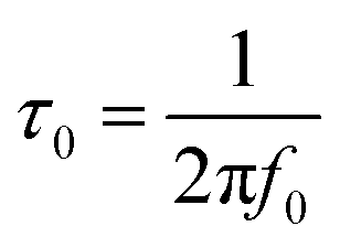 | (15) |
The relaxation time constant represents the transition from purely resistive to purely capacitive behavior for an electrochemical capacitor,79 and can be compared to a τ0 for ∼10 s for activated carbon supercapacitors and ∼1 ms for aluminum electrolytic capacitors.19
Furthermore, the value of τ0 can also be determined through scrutiny of the complex capacitance where valuable information is obtained through analysis of the real capacitance (C′) and imaginary capacitance (C′′) against the frequency (i.e. C′ versus f and −C′′ versus f). These are calculated using eqn (16) and (17), which are derived from the relationship C = C′ − jC′′.79
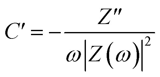 | (16) |
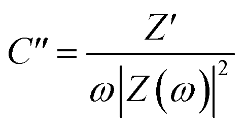 | (17) |
On the plot of −C′′ versus f, τ0 is taken as the frequency which gives the peak maximum.69,79
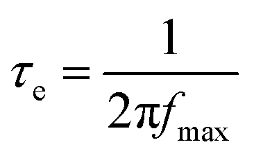
Similar to this, analysis of the Bode phase angle plot can provide valuable kinetic information for more materials than just capacitor-like systems. For example, the peak maximum at intermediate frequencies (fmax) in the Bode phase angle plot allow the determination of the electron recombination time (τe) for DSSCs through eqn (18).23,24
 | (18) |
The same type of analysis could be used for SAMs experiencing pseudocapacitance to calculate the electron transport constant (kET) using eqn (19).17
| kET = πfmax | (19) |
Conclusions
This manuscript reviewed the scope of EIS analysis for materials research to attract more researchers to EIS studies and to expand their knowledge of this technique. Main graphical methods to analyze EIS data (the Nyquist, Bode phase angle, and Bode magnitude plots) were introduced. In addition, capacitance, normalized capacitance and Randles plots were discussed in detail. It is noted that many of the graphical methods presented here provide the same parameters or results. For example, Bode phase angle plots, Nyquist plots, and capacitance plots can all be used to study capacitive behavior. Additionally, kinetic information can be obtained through a series of plots (Nyquist, Bode phase angle, and complex capacitance plots). Further, RΣ calculations and normalized capacitance plots can both be used to monitor changes of the internal resistance during durability cycling. Therefore, we hope readers recognize that not each parameter and graphical analysis must be completed for every material's characterization. On the contrary, there is a great number of EIS analyses that can be executed, and the choice of graphical analysis depends on the specific material being analyzed.Furthermore, the scope of the relevant theory behind each graphical analysis and calculation was included. This was reinforced with an additional introductory theory to EIS. Finally, recent literature examples highlighting applications of the EIS technique for characterization and performance studies of novel functional materials were discussed. Despite EIS being able to offer unmatched information about the surficial properties of an electrochemical material, EIS is commonly overlooked as a leading characterization technique. There is enormous value in EIS analysis for materials characterization, and thus, we hope that with our all-in-one guide containing the quintessence of EIS theory and methods of graphical analysis (EIS data plots and equations), new users to EIS will feel confident to pursue the EIS analysis, and experienced researchers will learn some new tricks to fully utilize the technique to get invaluable unique information on the conductive materials under investigation.
Author contributions
NOL conceived the concept for this review, designed the images and wrote the initial manuscript draft. OZ supported the writing, structuring and revisions of the manuscript. EBE contributed valuable insights to the EIS theory, proofreading and revisions of the manuscript.Conflicts of interest
There are no conflicts to declare.Acknowledgements
NOL acknowledges funding support from the Natural Sciences and Engineering Research Council of Canada's (NSERC) Alexander Graham Bell Canada Graduate Scholarship-Doctoral, and Ontario Tech University's Electrochemical Materials Lab for providing space to investigate electrochemical impedance spectroscopy.Notes and references
- J. Wood, Mater. Today, 2008, 11, 40–45 CrossRef CAS.
- M. Itagaki, S. Suzuki, I. Shitanda and K. Watanabe, Electrochem, 2007, 75, 649–655 CrossRef CAS.
- R. P. Janek and W. R. Fawcett, Langmuir, 1998, 14, 3011–3018 CrossRef CAS.
- R. Giannuzzi, M. Manca, L. De Marco, M. R. Belviso, A. Cannavale, T. Sibillano, C. Giannini, P. D. Cozzoli and G. Gigli, ACS Appl. Mater. Interfaces, 2014, 6, 1933–1943 CrossRef CAS PubMed.
- J. Wang, X. Li, Z. Wang, H. Guo, B. Huang, Z. Wang and G. Yan, J. Solid State Electrochem., 2015, 19, 153–160 CrossRef CAS.
- T. Dhandayuthapani, R. Sivakumar, R. Ilangovan, C. Gopalakrishnan, C. Sanjeeviraja, A. Sivanantharaja and R. Hari Krishna, J. Solid State Electrochem., 2018, 22, 1825–1838 CrossRef CAS.
- N. O. Laschuk, A. Obua, I. I. Ebralidze, H. Fruehwald, J. Poisson, J. G. Egan, F. Gaspari, E. B. Easton and O. V. Zenkina, ACS Appl. Electron. Mater., 2019, 1, 1705–1717 CrossRef CAS.
- J. Huang, Electrochim. Acta, 2018, 281, 170–188 CrossRef CAS.
- V. Ganesh, S. K. Pal, S. Kumar and V. Lakshminarayanan, J. Colloid Interface Sci., 2006, 296, 195–203 CrossRef CAS PubMed.
- D. Nkosi, J. Pillay, K. I. Ozoemena, K. Nouneh and M. Oyama, Phys. Chem. Chem. Phys., 2010, 12, 604–613 RSC.
- A. Muthurasu and V. Ganesh, J. Colloid Interface Sci., 2012, 374, 241–249 CrossRef CAS PubMed.
- S. A. Pauline, U. M. Kamachi and N. Rajendran, Mater. Chem. Phys., 2013, 142, 27–36 CrossRef.
- F. Fasmin and R. Srinivasan, J. Electrochem. Soc., 2017, 164, H443–H455 CrossRef CAS.
- L. Manjakkal, E. Djurdjic, K. Cvejin, J. Kulawik, K. Zaraska and D. Szwagierczak, Electrochim. Acta, 2015, 168, 246–255 CrossRef CAS.
- A. R. C. Bredar, A. L. Chown, A. R. Burton and B. H. Farnum, ACS Appl. Energy Mater., 2020, 3, 66–98 CrossRef CAS.
- E. P. Randviir and C. E. Banks, Anal. Methods, 2013, 5, 1098–1115 RSC.
- B. P. G. Silva, D. Z. de Florio and S. Brochsztain, J. Phys. Chem. C, 2014, 118, 4103–4112 CrossRef CAS.
- L. Noč, M. Ličen, I. D. Olenik, R. S. Chouhan, J. Kovač, D. Mandler and I. Jerman, Sol. Energy Mater. Sol. Cells, 2021, 223, 110984 CrossRef.
- J. Zhang, H. Feng, Q. Qin, G. Zhang, Y. Cui, Z. Chai and W. Zheng, J. Mater. Chem. A, 2016, 4, 6357–6367 RSC.
- V. K. Mariappan, K. Krishnamoorthy, P. Pazhamalai, S. Sahoo and S.-J. Kim, Electrochim. Acta, 2018, 265, 514–522 CrossRef CAS.
- J. Yao, Y. Jia, Q. Han, D. Yang, Q. Pan, S. Yao, J. Li, L. Duan and J. Liu, Nanotechnology, 2021, 32, 185401 CrossRef CAS PubMed.
- S. B. Dhavale, V. L. Patil, S. A. Beknalkar, A. M. Teli, A. H. Patil, A. P. Patil, J. C. Shin and P. S. Patil, J. Colloid Interface Sci., 2021, 588, 589–601 CrossRef CAS PubMed.
- W. Li, Y. Wu, Q. Zhang, H. Tian and W. Zhu, ACS Appl. Mater. Interfaces, 2012, 4, 1822–1830 CrossRef CAS PubMed.
- C.-H. Shan, H. Zhang, W.-L. Chen, Z.-M. Su and E.-B. Wang, J. Mater. Chem. A, 2016, 4, 3297–3303 RSC.
- N. Dimov, K. Fukuda, T. Umeno, S. Kugino and M. Yoshio, J. Power Sources, 2003, 114, 88–95 CrossRef CAS.
- S. R. Nayak, K. N. S. Mohana, M. B. Hegde, K. Rajitha, A. M. Madhusudhana and S. R. Naik, J. Alloys Compd., 2021, 856, 158057 CrossRef CAS.
- H. Khatoon, S. Iqbal and S. Ahmad, New J. Chem., 2019, 43, 10278–10290 RSC.
- R. N. Jenjeti, R. Kumar and S. Sampath, J. Mater. Chem. A, 2019, 7, 14545–14551 RSC.
- S. Zhu, A. Xie, B. Wei, X. Tao, J. Zhang, W. Peng, C. Liu, L. Gu, C. Xu and S. Luo, New J. Chem., 2020, 44, 9288–9297 RSC.
- R. Jurczakowski, C. Hitz and A. Lasia, J. Electroanal. Chem., 2004, 572, 355–366 CrossRef CAS.
- J. He, Z. Hu, J. Zhao, P. Liu, X. Lv, W. Tian, C. Wang, S. Tan and J. Ji, Chem. Eng. Sci., 2021, 243, 116774 CrossRef CAS.
- T. Majumder, D. Das, S. Jena, A. Mitra, S. Das and S. B. Majumder, J. Alloys Compd., 2021, 879, 160462 CrossRef CAS.
- N. O. Laschuk, I. I. Ebralidze, J. Poisson, J. G. Egan, S. Quaranta, J. T. Allan, H. Cusden, F. Gaspari, F. Naumkin, E. B. Easton and O. V. Zenkina, ACS Appl. Mater. Interfaces, 2018, 10, 35334–35343 CrossRef CAS PubMed.
- S. Shen, L. Yan, K. Song, Z. Lin, Z. Wang, D. Du and H. Zhang, RSC Adv., 2020, 10, 42008–42013 RSC.
- S. M. A. Mokhtar, E. A. de Eulate, V. Sethumadhavan, M. Yamada, T. W. Prow and D. R. Evans, J. Appl. Polym. Sci., 2021, e51314 CrossRef.
- E. Verpoorten, G. Massaglia, C. F. Pirri and M. Quaglio, Sensors, 2021, 21, 4110 CrossRef PubMed.
- S. Mahalingam, S. Ayyaru and Y. H. Ahn, Chemosphere, 2021, 278, 130426 CrossRef CAS PubMed.
- M. A. Ali, C. Hu, S. Jahan, B. Yuan, M. S. Saleh, E. Ju, S. J. Gao and R. Panat, Adv. Mater., 2021, 33, 2006647 CrossRef CAS PubMed.
- M. Z. Rashed, J. A. Kopechek, M. C. Priddy, K. T. Hamorsky, K. E. Palmer, N. Mittal, J. Valdez, J. Flynn and S. J. Williams, Biosens. Bioelectron., 2021, 171, 112709 CrossRef CAS PubMed.
- S.-M. Park and J.-S. Yoo, Anal. Chem., 2003, 75, 455A–461A CAS.
- G. Z. Chen, Int. Mater. Rev., 2016, 62, 173–202 CrossRef.
- M. Cimenti, A. C. Co, V. I. Birss and J. M. Hill, Fuel Cells, 2007, 7, 364–376 CrossRef CAS.
- N. Elgrishi, K. J. Rountree, B. D. McCarthy, E. S. Rountree, T. T. Eisenhart and J. L. Dempsey, J. Chem. Educ., 2017, 95, 197–206 CrossRef.
- J. Castello, R. Garcia-Gil and J. M. Espi, Measurement, 2008, 41, 631–636 CrossRef.
- V. S. Simi and N. Rajendran, Mater. Charact., 2017, 129, 67–79 CrossRef CAS.
- J. Aguedo, L. Lorencova, M. Barath, P. Farkas and J. Tkac, Chemosensors, 2020, 8, 127 CrossRef CAS.
- M. I. Muglali, A. Bashir, A. Terfort and M. Rohwerder, Phys. Chem. Chem. Phys., 2011, 13, 15530–15538 RSC.
- L. Wu, F. Camacho-Alanis, H. Castaneda, G. Zangari and N. Swami, Electrochim. Acta, 2010, 55, 8758–8765 CrossRef CAS.
- T. Alshahrani, RSC Adv., 2021, 11, 9797–9806 RSC.
- J. K. Bhattarai, Y. H. Tan, B. Pandey, K. Fujikawa, A. V. Demchenko and K. J. Stine, J. Electroanal. Chem., 2016, 780, 311–320 CrossRef CAS PubMed.
- S. I. Ahmed and M. M. S. Sanad, J. Alloys Compd., 2021, 861, 157962 CrossRef CAS.
- R. Ahmad, N. O. Laschuk, O. V. Zenkina, I. I. Ebralidze and E. B. Easton, ChemElectroChem, 2021, 8, 2193–2204 CrossRef CAS.
- N. O. San Keskin, F. Deniz and H. Nazır, RSC Adv., 2020, 10, 39901–39908 RSC.
- Z. Siroma, N. Fujiwara, S.-i. Yamazaki, M. Asahi, T. Nagai and T. Ioroi, J. Electroanal. Chem., 2020, 878 CrossRef CAS.
- G. Li and P. G. Pickup, Phys. Chem. Chem. Phys., 2000, 2, 1255–1260 RSC.
- Y. Liu, M. W. Murphy, D. R. Baker, W. Gu, C. Ji, J. Jorne and H. A. Gasteiger, J. Electrochem. Soc., 2009, 156, B970–B980 CrossRef CAS.
- F. S. Saleh and E. B. Easton, J. Electrochem. Soc., 2012, 159, B546–B553 CrossRef CAS.
- O. Reid, F. S. Saleh and E. B. Easton, Electrochim. Acta, 2013, 114, 278–284 CrossRef CAS.
- E. Trollund, P. Ardiles, M. J. Aguirre, S. R. Biaggio and R. C. Rocha-Filho, Polyhedron, 2000, 19, 2303–2312 CrossRef CAS.
- Q. Guo, J. Li, B. Zhang, G. Nie and D. Wang, ACS Appl. Mater. Interfaces, 2019, 11, 6491–6501 CrossRef CAS PubMed.
- L. Yuan, X.-H. Lu, X. Xiao, T. Zhai, J. Dai, F. Zhang, B. Hu, X. Wang, L. Gong, J. Chen, C. Hu, Y. Tong, J. Zhou and Z. L. Wang, ACS Nano, 2012, 6, 656–661 CrossRef CAS PubMed.
- T. Ye, Y. Sun, X. Zhao, B. Lin, H. Yang, X. Zhang and L. Guo, J. Mater. Chem. A, 2018, 6, 18994–19003 RSC.
- M. Shimizu, T. Ohnuki, T. Ogasawara, T. Banno and S. Arai, RSC Adv., 2019, 9, 21939–21945 RSC.
- M. Lefebvre, Z. Qi, D. Rana and P. G. Pickup, Chem. Mater., 1999, 11, 262–268 CrossRef CAS.
- E. B. Easton, H. M. Fruehwald, R. Randle, F. S. Saleh and I. I. Ebralidze, Carbon, 2020, 162, 502–509 CrossRef CAS.
- D. Ortiz-Aguayo and M. del Valle, Sensors, 2018, 18, 354 CrossRef PubMed.
- B. P. G. Silva, B. Tosco, D. Z. de Florio, V. Stepanenko, F. Würthner, J. F. Q. Rey and S. Brochsztain, J. Phys. Chem. C, 2020, 124, 5541–5551 CrossRef CAS.
- R. Acheampong, R. Alipour Moghadam Esfahani, R. B. Moghaddam and E. B. Easton, J. Electrochem. Soc., 2020, 167, 044516 CrossRef CAS.
- W.-W. Liu, Y.-Q. Feng, X.-B. Yan, J.-T. Chen and Q.-J. Xue, Adv. Funct. Mater., 2013, 23, 4111–4122 CrossRef CAS.
- G. Piłatowicz, A. Marongiu, J. Drillkens, P. Sinhuber and D. U. Sauer, J. Power Sources, 2015, 296, 365–376 CrossRef.
- O. O. Reid, F. S. Saleh and E. B. Easton, ECS Trans., 2014, 61, 25–32 CrossRef CAS.
- H. M. Fruehwald, R. B. Moghaddam, P. D. Melino, I. I. Ebralidze, O. V. Zenkina and E. B. Easton, Catal. Sci. Technol., 2021, 11, 4026–4033 RSC.
- N. Laschuk, I. Ebralidze, E. B. Easton and O. Zenkina, ACS Appl. Energy Mater., 2021, 4, 3469–3479 CrossRef CAS.
- N. O. Laschuk, R. Ahmad, I. I. Ebralidze, J. Poisson, F. Gaspari, E. B. Easton and O. V. Zenkina, Mater. Adv., 2021, 2, 953–962 RSC.
- Y. Xu, S. Wang, H. Peng, Z. Yang, D. J. Martin, A. Bund, A. K. Nanjundan and Y. Yamauchi, ChemElectroChem, 2019, 6, 2456–2463 CrossRef CAS.
- F. Matemadombo and T. Nyokong, Electrochim. Acta, 2007, 52, 6856–6864 CrossRef CAS.
- D. Dong, W. Wang, G. Dong, F. Zhang, H. Yu, Y. He and X. Diao, RSC Adv., 2016, 6, 111148–111160 RSC.
- M. Urso, S. Tumino, E. Bruno, S. Bordonaro, D. Marletta, G. R. Loria, A. Avni, Y. Shacham-Diamand, F. Priolo and S. Mirabella, ACS Appl. Mater. Interfaces, 2020, 12, 50143–50151 CrossRef CAS PubMed.
- V. Ganesh, S. Pitchumani and V. Lakshminarayanan, J. Power Sources, 2006, 158, 1523–1532 CrossRef CAS.
Footnote |
| † Typical impedance analysis software includes Scribner©'s ZView® with ZPlot®, and similar software from Biologic©, Gamry©, and Pine Instruments©. |
| This journal is © The Royal Society of Chemistry 2021 |