
 Open Access Article
 This Open Access Article is licensed under a Creative Commons Attribution-Non Commercial 3.0 Unported Licence
Revealing the impact of strontium doping on the optical, electronic and electrical properties of nanostructured 2H-CuFeO2 delafossite thin films†
Hamza Shaili *a,
Elmehdi Salmanib,
Mustapha Beraichc,
Abderrahim Elhata,
Mustapha Rouchdia,
Mhamed Taibid,
Hamid Ez-Zahraouyb,
Najem Hassanaina and
Ahmed Mzerda
*a,
Elmehdi Salmanib,
Mustapha Beraichc,
Abderrahim Elhata,
Mustapha Rouchdia,
Mhamed Taibid,
Hamid Ez-Zahraouyb,
Najem Hassanaina and
Ahmed Mzerda
aGroup of STCE-Energy Research Center (ERC), Faculty of Sciences, Mohammed V University, B. P. 1014, Rabat, Morocco. E-mail: hamza.shaili13@gmail.com; Tel: +21 2604710051
bLaboratory of Condensed Matter and Interdisciplinary Sciences Department of Physics, Faculty of Sciences, Mohammed V University, Rabat, Morocco
cLaboratory of Physics of Condensed Matter, Department of Physics, Ibn Tofail University, Kenitra, Morocco
dCSM, LPCMIO, Ecole Normale Supérieure, Mohammed V University, Rabat, Morocco
First published on 26th July 2021
Abstract
Delafossite materials are considered to be a promising range of transparent conductive oxides for optoelectronic applications. The complications that have held back their implementation in practical devices lie in the complex growth methods that are required and in the formation of undesirable secondary phases. Herein, a fast, simple, and low-cost deposition method allowing the deposition of high-quality 2H-CuFeO2 nanostructured thin films is employed. The effect of Sr doping on the properties of spray-coated CuFeO2 thin film annealed at 850 °C is reported. X-ray diffraction (XRD) analysis revealed the delafossite structures of all the samples corresponding to the 2H-CuFeO2 phase. The lattice spacing decreased with increasing substitution of Sr at the Cu site. Raman analysis further authenticated the structural results collected via XRD analysis. Surface scanning using field-emission scanning electron microscopy revealed the formation of nanostructured CuFeO2 thin film possessing high crystalline quality, with the nanocrystal size increasing as the dopant content was increased. Energy-dispersive X-ray analysis allowed the quantification of the elements content via determining the ratios of the main elements as well as the dopant content in each sample. The optical properties of the samples showed strong light absorption in the visible region with a decrease in the band gap values with Sr insertion. First-principles calculations using density functional theory (DFT) were conducted to strengthen the experimental findings regarding the nature of the bonds in the hexagonal lattice of the CuFeO2 compound and the effect of Sr doping on its characteristics. The electrical properties measured at room temperature revealed p-type conductivity with tunable resistivity, while the samples displayed increased electron mobility as a function of the dopant content. Consequently, our work introduced an efficient and cost-effective synthesis route for the preparation of high-quality nanostructured 2H-CuFeO2 thin films, paving the way to facilitate further device applications.
1. Introduction
In the past few years, there has been great demand for the development of a new and more efficient type of transparent conductive oxides (TCOs) for numerous fields of application. Several TCOs, such as ZnO, In2O3, and SnO2, have been investigated extensively in recent decades and employed in industrial applications, as they demonstrate good performance in various optoelectronic devices including LEDs, solar cells, and gas sensors.1–4 The need to enhance the efficiency of such devices has forced the research community to search for and develop other advanced types of TCOs that have the capability to boost device efficiency via enhanced optical and electrical properties.One of the most promising classes of TCO candidates that has been studied and developed is the copper-based delafossite oxides CuMO2 (M = Fe, Cr, Al, Ga, Mn, Co…), which exhibit interesting optical and electrical properties compared to conventional TCOs. This interesting type of semiconducting oxides has been considered for several applications, including photocatalysis for solar energy conversion,5 luminescent materials,6 thermoelectrics,7 gas sensors8, batteries9, and photocathodes to produce hydrogen via water splitting.10 Herein, the emphasis will be on the CuFeO2 compound, which is composed of earth-abundant elements and has stable structural properties at room temperature and interesting electrical properties.7 CuFeO2 also offers good optical properties, a tunable band gap, and controllable conductivity, making it suitable for several applications such as anodes in lithium-ion batteries11 and in photovoltaics.12
According to the literature, CuFeO2 is a p-type semiconductor that crystallizes in two different structures, the rhombohedral (3R)-type13 and the hexagonal (2H)-type structure.14 The majority of papers that have reported the effective synthesis of CuFeO2, whether in nanoparticle or thin-film form, indicated a structure corresponding to the rhombohedral 3R-CuFeO2 phase or a mixture of the two phases. Only a limited number of papers have reported the successful synthesis of the 2H-CuFeO2 phase, and several difficulties were associated with the process.12,15 Furthermore, numerous attempts to engineer the physical and chemical properties of the CuFeO2 compound through a doping process using a variety of dopant elements have been conducted.16–18 Considerable attention has been paid to the use of alkali elements to adjust the characteristics of CuFeO2 for various fields of application. Anna Wuttig et al. reported Mg-doped CuFeO2 and tested its compatibility as a photocathode to optimize CO2 reduction.19 Qiang Gao et al. reported Ca-doped CuFeO2 and the modification of its initial properties.20 To the best of our knowledge, there are no reports describing tuning the properties of the material CuFeO2 using strontium either experimentally or through first-principles calculations.
3R-CuFeO2 thin films have been synthesized via several physical and chemical methods including pulsed laser deposition,21 radiofrequency magnetron sputtering,22 aerosol-assisted chemical vapor deposition,23 electrodeposition,24 spray pyrolysis,25 and spin-coating.26 In most previous attempts to prepare CuFeO2 in thin-film form, complex and expensive routes were utilized, which poses a major drawback for practical applications. So far, only a few attempts have been made to grow a CuFeO2 thin film corresponding to the hexagonal phase, especially through chemical deposition methods. Therefore, in the present paper, we aimed to develop a much simpler and faster chemical synthesis approach to obtain this material in thin-film form and to study its properties in detail. Another important objective of this work was to identify the impact of strontium doping on the characteristics of CuFeO2, with particular interest in the optical and electrical properties. To strengthen the quality of the present work, a theoretical part employing density functional theory (DFT) calculations was included to examine the effect of Sr doping on the electronic and optical properties of the pristine CuFeO2 lattice. This will allow a better understanding of the bonds formed between the atoms and their interactions, as well as the effects of the defects induced by doping on the electronic properties of the initial lattice.
2. Experimental details
2.1 Solution preparation and thin film synthesis
A typical synthesis process required the preparation of clean and stoichiometric aqueous solutions to deposit the pure and Sr-doped CuFeO2 thin films by mixing 0.02 mol of copper(I) chloride (CuCl, 98% purity) and 0.02 mol of iron(III) chloride (FeCl3, 99% purity) in 25 ml of distilled water at room temperature. A few drops of nitric acid (HNO3) were added, and the mixture was kept under vigorous magnetic stirring at 60 °C for 1 h for homogenization. For doping, strontium nitrate (Sr(NO3)2, 98% purity) was added to the precursor solutions in two different concentrations (x = 3 and 5 at%). The solution was transferred to a deposition chamber equipped with an ultrasonic spray set-up (SONAER-Ultrasonics) set at a frequency of 130 kHz and an applied power of 2.8 W.27–29 Double-side polished fused-silica-quartz glass sheets (1 cm × 1.5 cm) were selected as the substrates. The substrates were ultrasonically cleaned with distilled water, ethanol, and acetone consecutively for 15 minutes and finally dried in an air stream. The solution flow rate was fixed at 0.9 ml min−1 and compressed air was used as the carrier gas. The substrates were placed horizontally on the surface of a hot plate at a distance of 12 cm below the spray nozzle, as depicted in Fig. 1. The hot plate was initially heated at a slow rate to reach a temperature of 250 °C controlled using a thermocouple. Multiple attempts were performed to reach the optimal temperature conditions. The deposition time was approximately 25 min. Finally, the prepared films were placed in a furnace and calcined in air at 850 °C for 2 h with a temperature step of 15 °C min−1 to form the correct phase. All the prepared thin films were found to be highly stable under standard conditions, with excellent adherence to the substrates. The color of the sample remained dark brown throughout the doping process.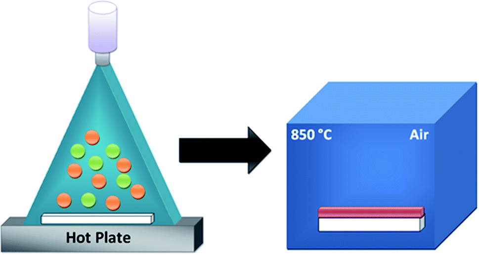 | ||
| Fig. 1 A schematic diagram of the ultrasonic spray deposition method and the annealing process in the furnace. | ||
2.2 Characterization
XRD analysis was performed to identify the phase and crystalline structure of the obtained samples using a Bruker D8 Discover Advanced Diffractometer with Cu Kα radiation at a wavelength of λ = 0.154056 nm. The XRD data were collected over the range 30° < 2θ < 70° with a step of 0.008° and an integration time of 0.25 s. Raman measurements were recorded at room temperature using a Raman spectrometer microscope (DXR2; Thermo Scientific) with a laser excitation wavelength of 633 nm. The effect of the doping process on the surface morphology and elemental composition of the thin films was examined using field emission scanning electron microscopy (FE-SEM, Quanta 200-FEI) and energy-dispersive X-ray spectroscopy (EDX, Hitachi) with a 15 kV accelerating voltage, respectively. Atomic mapping was also performed to quantify and observe the distribution of the elements on the film surfaces. Optical properties were determined using a UV-Vis spectrophotometer (Lambda 900 UV/VIS/NIR Spectrophotometer) from 200 nm to 1000 nm. The electrical properties of the films were measured at room temperature using an ECOPIA-AMP55T Hall effect measurement system in the van der Pauw configuration with the presence of a magnetic field.3. Computational methods
Ab initio calculations were carried out via density functional theory using the Korringa–Kohn–Rostoker (KKR) method with the coherent potential approximation (CPA). The 3 d-related electronic states were modulated using the self-interaction corrected (SIC) approach developed by Toyoda.30 The SIC approach was utilized to obtain a more realistic description of the disordered local moments of the materials under investigation, as described previously.31 For the parameterization of the exchange energy, the generalized gradient approximation of Perdew, Burke and Ernzerhof (GGA-PBE) was employed; the SIC approach was included in the KKR-CPA-SIC-GGA package as implemented in MACHIKANEYAMA2002.31 500 K-points in the whole first Brillouin zone were taken into account, and the scalar relativistic approximation was also incorporated. The SIC-GGA approximation allows the calculation to be more precise than the regular GGA approximation, resulting in an enhancement of the photoemission spectra. In the present work, we are most interested in the hexagonal structure of CuFeO2 with the space group P63/mmc (no. 194). For the calculations of the doped material, a fraction of the Cu atoms were randomly replaced by Sr atoms. The electronic valence configurations for each element were: Cu-3d10 4s1, Fe-3d6 4s2, O-2s2 2p4 and Sr-3d10 4s2 4p6 5s2. The total energy minimization was performed using the appropriate unit cells of a hexagonal lattice with the P63/mmc space group. In the current calculations, we fixed the parameters v and b/a, which are determined by the geometry. The internal parameter u and the c/a ratio were obtained via the energy minimization for the pure compound CuFeO2 and were fixed for the Cu1−2xSrxFeO2 alloys. All calculations were performed at T = 0 K from the total energy fitted to the Murnaghan equation. Lattice vibrations, finite temperature effects, and relativistic corrections were not considered in the current work. The electronic and optical properties of the pure and Sr-doped CuFeO2 were calculated using a stable hexagonal structure that also conforms to the P63/mmc space group.4. Results and discussion
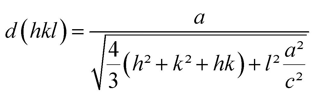
The XRD patterns of the pure and Sr-doped CuFeO2 thin films annealed at 850 °C are illustrated in Fig. 2. The results reveal that the undoped film has a polycrystalline nature, with three peaks located at 31.67°, 34.72°, and 37.17° corresponding to the planes (004), (101), and (012), respectively. All peaks corresponded to the hexagonal (P63/mmc) structure of CuFeO2, matching correctly with the standard JCPDS data (PDF no. 79-1546). No peaks related to any impurity, such as Sr clusters, or peaks linked to copper or ferrite secondary phases were observed. Previous reports indicated that the formation of the 2H-CuFeO2 phase is difficult due to several aspects.12–14 Furthermore, several reports indicated that in the synthesis process of the CuFeO2 compound, the resulting compounds are always a mixture of the 2H-CuFeO2 and 3R-CuFeO2 phases, with a higher possibility of obtaining the majority of the peaks related to the rhombohedral structure. However, and despite the simplicity of the utilized method and the facile precursor preparation, we were able to successfully synthesize the 2H-CuFeO2 thin films with only peaks related to the corresponding phase. A preferential orientation along the (012) plane was observed for the pristine sample, while for the doped ones, it changed to the (101) plane. In terms of the effect of doping on the structural properties of the undoped film, little change was observed except for the partial disappearance of the peak located at 31.67°, which may be due to the internal defects and strain induced by the incorporation of the Sr fractions. The quality of the patterns and the intensity of the peaks were slightly affected by the doping; it can be observed that the peaks are slightly more intense and the phase quality is ameliorated in general. The lattice parameters were calculated by employing the equation below to investigate the crystallographic defects in the obtained structure and the influence of the integration of the dopant fraction on the lattice shape:
 | (1) |
The calculated lattice parameters are illustrated in Fig. 3a. The values of the lattice constants (a and c) for the pristine sample are in agreement with previously reported results for the 2H-CuFeO2 structure.12,14 The lattice parameters show similar behavior in which both a and c decrease upon Sr addition. This decrease may be attributed to several factors, including the concentration of the dopant, defects (vacancies, interstitial, and dislocation), external strain developed due to the calcination temperature, and the difference between the ionic radii of Sr2+ (1.18 Å) and Cu+ (0.77 Å), which was observed earlier via the increasing intensities. The structure remains hexagonal and is not altered by the addition of different amounts of strontium into the CuFeO2 lattice.
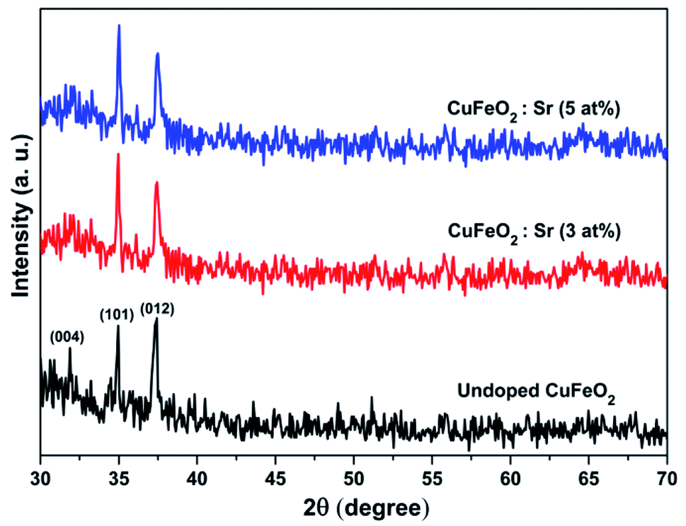 | ||
| Fig. 2 XRD patterns of pure and Sr-doped 2H-CuFeO2 thin films. | ||
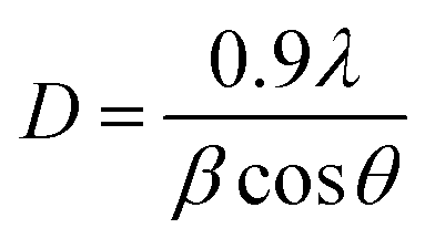
Furthermore, the effect of strontium incorporation on the crystallite size of the nanostructured CuFeO2 thin film was investigated by employing the Debye–Scherrer formula:
 | (2) |
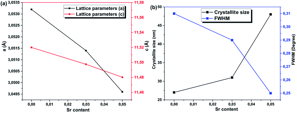 | ||
| Fig. 3 Variations of the calculated CuFeO2 (a) lattice constants and (b) crystallite size and FWHM values as a function of the Sr content. | ||
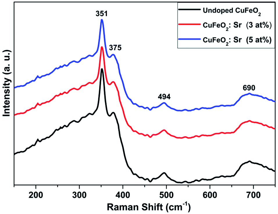
Typical Raman analysis was performed at room temperature to further analyze the purity of the as-synthesized films, as well as to examine the homogeneity and crystallinity of the samples and understand the change in cation ordering. Raman analysis allows the determination of local structures and identification of changes in cation ordering of the samples. Fig. 4 presents the Raman modes obtained for the pristine and Sr-doped CuFeO2 samples. Three major vibrational modes were detected at 351, 375 and 690 cm−1, all of which were assigned to the 2H-CuFeO2 structure.21 The peaks at 351 and 690 cm−1 are assigned to Eg and A1g vibrational modes, respectively. The additional peak located at 495 cm−1 is generally attributed to non-zero wavevector phonons and is generated by the presence of crystalline defects.21 So far, only a few papers have reported the Raman analysis of CuFeO2 in the hexagonal structure. Y. Jin et al. reported the first Raman analysis of hexagonal CuFeO2 nanoplates and recorded almost the same major modes.12 It can be noted that after the first dopant fraction was introduced, a small decrease in the intensities of the bands was detected with no change in the modes as illustrated in Fig. S2.† The two main modes show a slight shift toward higher wavenumber in comparison to those in the undoped sample, indicating the effective insertion of Sr2+ cations in the place of Cu+, which consequently impacts the Cu–O bonds. The decrease in the intensities became more notable as the Sr content increased, but the modes were maintained. Indeed, the results suggest the high crystallinity of the deposited films with a consistent structure throughout the doping process. Hence, the Raman analysis further confirms the obtained phase and indicates the high quality of the prepared samples.
 | ||
| Fig. 4 Raman spectra of pure and Sr-doped CuFeO2 nanostructured thin films at room temperature. | ||
It is well known that morphological properties strongly impact the efficiency and construction of optoelectronic devices. Therefore, to be considered for further optoelectronic applications, a full and thorough assessment of the surface quality must take place. The morphology of the synthesized films was examined by means of field emission scanning electron microscopy (FE-SEM) and energy dispersive spectroscopy (EDX) to observe and evaluate the modifications induced by doping on the quality, grain size, and composition of the films, as shown in Fig. 5. It can be seen from Fig. 5a that the deposited samples exhibit a textured, uniform and homogeneous surface with an even distribution over the substrate. In addition, the micrographs in Fig. 5b–d show the formation of high-density quasi-hexagon-shaped grains with different sizes. An increase in the grain size was noted when the lower concentration of the dopant was introduced. At 5% Sr content, the grains became bigger and denser due to the expansion in the CuFeO2 lattice. This increase was observed earlier from the XRD data as a result of the difference in ionic radii, indicating agreement between the obtained results. It can be observed that the doping process enhances the quality of the obtained nanocrystals, which can have an immense effect on the transport properties of the film, particularly in terms of increasing its carrier mobility.
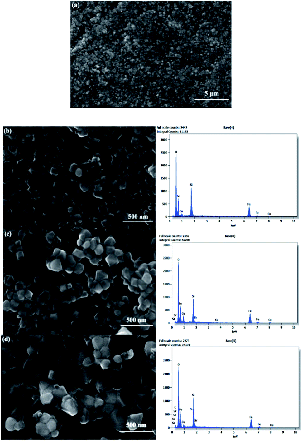 | ||
| Fig. 5 FE-SEM scanning images and associated EDX analyses of pure and Sr-doped CuFeO2 thin films. (a) A top view of the pristine CuFeO2 thin film and close views of the (b) 0%, (c) 3%, and (d) 5% Sr-doped CuFeO2 thin films. | ||
Moreover, EDX analysis was conducted to inspect the elemental composition of the prepared films, as presented in Fig. 6. The data illustrate the obtained percentages, with the presence of sufficient quantities of the main elements (Cu, Fe, and O). The ratios of the elements indicate the high purity and near-stoichiometric nature of the samples with rich oxygen content, as illustrated in Table S2.† In addition, the Si signal is detected from the quartz substrate as a result of the difference between the thickness of the film and the high EDX interaction volume and penetration depth of the electron beam. This may slightly reduce the accuracy of the quantitative analysis. The presence of the dopant Sr was confirmed in the doped films in varying quantities, depending on the percentage added. It can be noted that the ratios became slightly imbalanced as the doping element was introduced. Additionally, elemental atomic mapping was included to visualize the distribution of the elements on the resulting surfaces, allowing the quantification of each component with high precision. The mapping images in Fig. 6 once again demonstrate the presence of the main elements with a near-stoichiometric distribution. In addition, the images exhibit a uniform distribution of the elements with a higher concentration for the oxygen element and a small portion of the Sr element.
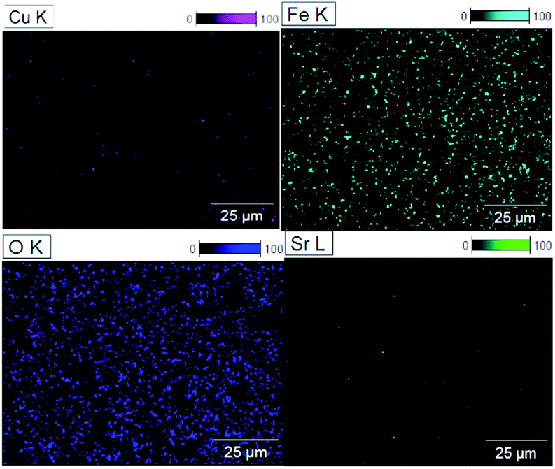 | ||
| Fig. 6 Atomic mapping (Cu, Fe, O, and Sr) images of Sr-doped CuFeO2 thin films. | ||
The UV-vis spectra of the pure and Sr-doped CuFeO2 thin films are presented in Fig. 7a. All the films exhibit strong absorption behavior in the UV light region (200–400 nm), with a notable increase in the visible region, which continues to increase exponentially as the wavelength increases into the near-infrared (NIR) region. It can be noted that the absorption edge of the doped films is shifted toward higher wavelength, especially for the 5% Sr-doped CuFeO2 film. Furthermore, when the dopant fractions were introduced, the absorption increased slightly, demonstrating that strontium increased the absorption of the metal oxide, as has been reported previously.33 To summarize, strontium doping effectively enhanced the quality of the films, particularly for the 3 at% Sr film, which directly impacted their photon absorption ability. The band gaps of the pristine and Sr-doped CuFeO2 were calculated using the Tauc plot according to the equation:
 | (3) |
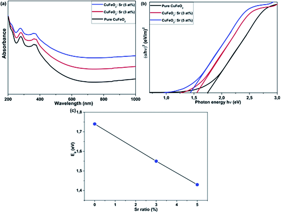 | ||
| Fig. 7 (a) Recorded optical absorbance as a function of wavelength. (b) Plots of (αhν)1/2 versus hν and (c) the band gap variations of pristine and Sr-doped CuFeO2 nanostructured thin films. | ||
Ab initio calculations were performed to uncover the nature of the bonds formed between the different elements and to investigate the electronic properties and the effect of strontium incorporation on the pristine CuFeO2 lattice. In order to conduct a comparative study, the doping concentrations selected for DFT calculations were the same as those used in the experiment. Fig. 8 shows the unit cell of the pristine CuFeO2 compound with the positioning of each atom. In general, an idealized solid exhibits perfect periodicity, which allows the theoretical calculations to be restricted to just one unit cell as long as the bulk properties are considered, which is validated in the calculation method employed in the present work. To the best of our knowledge, this is the first report of DFT calculations on the properties of CuFeO2 in the hexagonal structure. Doping a system with non-magnetic impurities commonly leads to a non-magnetic system. Therefore, in this work, we chose to perform doping with a non-magnetic element (Sr2+ ions) to avoid any augmentation of the magnetic behavior of the system and improve the properties of the material under investigation.
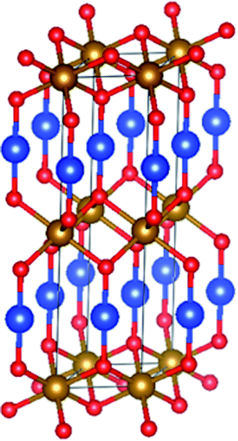 | ||
| Fig. 8 The crystal structure of CuFeO2 crystallizing in the hexagonal structure. Color code: Cu = blue, Fe = brown, O = red. | ||
Fig. 9 presents the spin-up and spin-down band structures calculated for the pristine CuFeO2 using both the GGA and GGA-SIC approximations. Defect-free CuFeO2 is a semiconductor with the valence-band maximum (VBM) and the conduction-band minimum (CBM) positioned at the Γ(0,0,0) point at the center of the Brillouin zone, indicating a direct-band-gap semiconductor nature. The band gaps were calculated to be 1.08 and 1.67 eV using the GGA and GGA-SIC approximations, respectively. The obtained band gap for GGA-SIC is in close agreement with previous experimental values.12 Furthermore, semi-conducting behavior can clearly be seen for the spin-up band structure, while the spin-down band structure is metallic in both approximations. A comparison of the calculated value with the band gap (1.75 eV) observed experimentally using the UV-vis spectrometer indicates the presence of point defects.
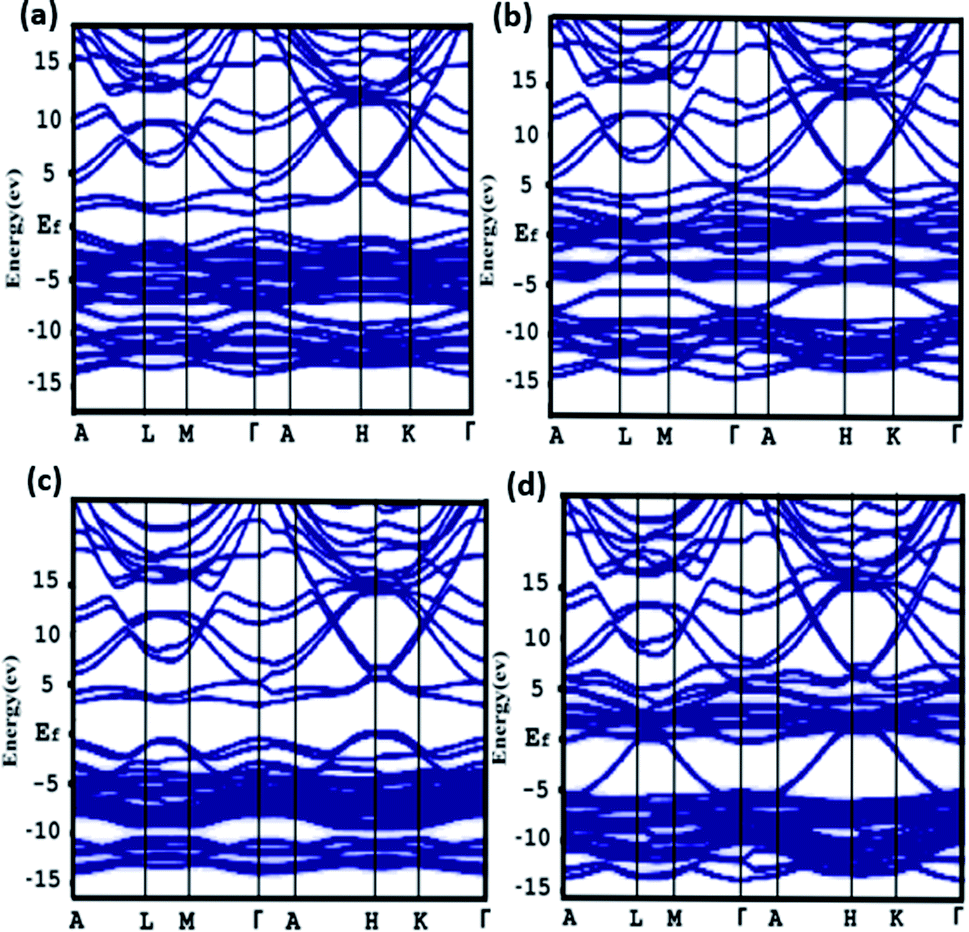 | ||
| Fig. 9 The band structure of 2H-CuFeO2 using the GGA-PBE ((a) spin-up and (b) spin-down) and GGA-SIC approximations ((c) spin-up and (d) spin-down). | ||
Usually, the regular GGA-PBE tends to underestimate the actual properties of the material under investigation, meaning that the exchange and the correlation effects in transition metal oxides are not considered. This leads to important self-interaction errors32. This can be clearly observed in the density of states calculated using the GGA-PBE approximation, while the GGA-SIC provided a value that was relatively closer to that collected from experimental measurements. This band gap increase is due to the delocalization of electrons in such materials and nonzero self-interaction errors of DFT. When a semiconductor is doped, the Fermi level tends to shift towards higher energy values, which can be explained by the fact that the doping process enhances the stability of the compound corresponding to the low energies. Fig. 10 displays the total and partial DOS (spin-up and -down) of the pristine and strontium-doped CuFeO2 using the GGA and GGA-SIC approximations. It can clearly be noted from Fig. 10a that for the GGA-PBE approximation, the spin-up and spin-down channels do not overlap, indicating the half-metallic behavior of the pristine structure. For that reason, the self-interaction corrected (SIC) was implemented to reduce this behavior to the greatest extent possible. The DOS in Fig. 10b also reveals that CuFeO2 acts as a half-metal, and the same behavior was noted for the spin-up channel. However, for the spin-down channel, the metallic behavior is greatly reduced due to the fact that the Fe band gap opened up with SIC correction. The conduction band minima (CB) of CuFeO2 are composed essentially of Fe-3d states with some overlap between Cu-3d and O-2p, while the valence band maxima (VB) are largely dominated by the Cu-3d states with a minor contribution from O-2p states. However, the contribution of the Cu-d states becomes prominent in the −0.5 to −0.3 eV zone. An important contribution was observed from the Sr-3d states as the dopant was induced, with increased domination of the Fe-3d states for both of the doping percentages. The band gap became narrower relative to that of pristine CuFeO2 and settled at 1.22 eV for 5 at% strontium content. In summary, first-principles calculations using DFT permitted an in-depth investigation of the properties of the hexagonal CuFeO2, as well as of the effect of Sr2+ incorporation in tuning the initial properties; the results were consistent with the experimental findings.
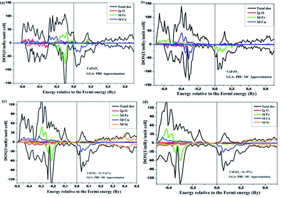 | ||
| Fig. 10 Calculated partial and total DOS for pure and Sr-doped CuFeO2: (a) 0% with GGA, (b) 0% with GGA-SIC, (c) 3% Sr content, and (d) 5% Sr content. | ||
Evaluation of the potentials of certain materials for optoelectronic applications relies heavily on their electrical properties. Thus, it is essential to determine the electrical properties of the prepared samples and the changes resulting from the alkali-element doping of the CuFeO2 films in order to enhance their properties and thereby evaluate their potential for further applications. For this purpose, the electrical properties of pure and Sr-doped CuFeO2 thin films were measured at room temperature to determine their semiconducting nature and to investigate the tunability of the conductivity and carrier mobility due to the strontium doping of the pristine CuFeO2 nanostructured films. Fig. 11 shows the electrical properties measured using the van der Pauw configuration and their variation as a function of the dopant content. The Hall coefficient (RH) measurements indicated the p-type nature of the CuFeO2 compound, as reported previously.20,22 The resistivity of the undoped CuFeO2 thin film was measured to be 4.95 Ω cm. An intense decrease in the electrical resistivity was observed at the lower doping percentage, manifesting the effective capability of Sr-doping to increase the conductivity of metal oxides. The resistivity value further decreased to settle at 3.5 Ω cm for 5 at% Sr content. The same tendency was observed for the carrier concentration, which decreased greatly due to the doping. Furthermore, the increased carrier mobility due to doping was suggested above from the SEM images, which showed an augmentation in grain size leading to an enhancement of the carrier mobility from 7.9 cm2 V−1 s−1 for the undoped sample to 12.1 cm2 V−1 s−1 for the 5 at% Sr sample. Hence, the prepared CuFeO2 thin film possessed superior electrical properties compared to other delafossite materials, with these enhanced characteristics being generated by the doping process.
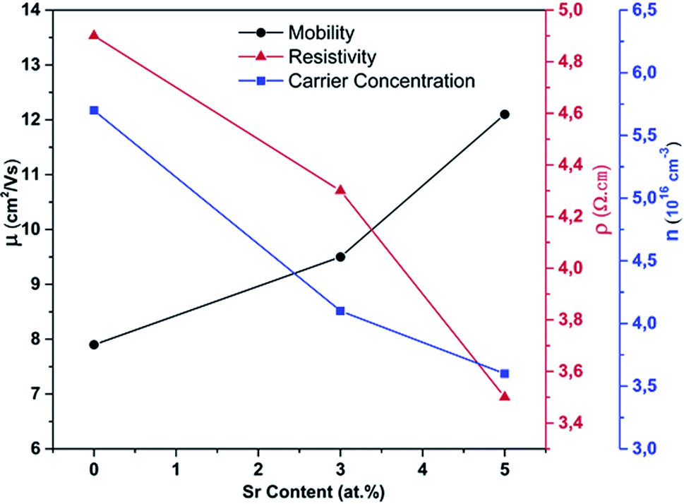 | ||
| Fig. 11 Resistivity, carrier concentration, and mobility of pure and Sr-doped CuFeO2 films as a function of the Sr content, measured at room temperature. | ||
5. Conclusions
High-quality nanostructured 2H-CuFeO2 thin films have been synthesized via employing a simple chemical route and facile precursor preparation. Several characterization tools were employed to analyze and verify the purity of the samples. Structural investigations revealed the successful synthesis of 2H-CuFeO2 thin films with no secondary phases. Morphological scanning showed that the doping process remarkably improved the quality of the resulting surfaces, with an even elemental distribution over the surfaces of the films. The optical band gap of the pure sample was estimated to be 1.75 eV and decreased as the dopant percentage increased, reaching 1.43 eV for 5 at% of strontium content. The band gap decrease due to Sr doping was further observed through first-principles calculations, which showed similar variations to those suggested by the experimental results. The electrical resistivity and carrier concentration of the pure film decreased as the dopant content was increased. The obtained results demonstrate the effectiveness of using a simple chemical route to produce high-quality single-phase nanostructured 2H-CuFeO2 thin films and the capability of strontium doping to enhance the properties of delafossite materials.Conflicts of interest
There are no conflicts to declare.Notes and references
- L. Zhu and Z. Wen, Room-temperature gas sensing of ZnO-based gas sensor: A review, Sens. Actuators, A, 2017, 267, 242–261 CrossRef CAS.
- Y. Chen, M. Qi, L. Zhang, C. Han, H. Gao, Y. Zhang and H. Yan, SnO2-based electron transporting layer materials for perovskite solar cells: A review of recent progress, J. Energy Chem., 2019, 35, 144–167 CrossRef.
- P. Prathap, A. S. Dahiya, M. Srivastava, S. K. Srivastava, B. Sivaiah, D. Haranath, R. Vandana, R. Srivastava, C. M. S. Rauthan and P. K. Singh, Anti-reflection In2O3 nanocones for silicon solar cells, Sol. Energy, 2014, 106, 102–108 CrossRef CAS.
- D.-K. Hwang, M.-S. Oh, J.-H. Lim and S.-J. Park, ZnO thin films and light-emitting diodes, J. Phys. D: Appl. Phys., 2007, 40, R387–R412 CrossRef CAS.
- Q.-L. Liu, Z.-Y. Zhao, R.-D. Zhao and J.-H. Yi, Fundamental properties of delafossite CuFeO2 as photocatalyst for solar energy conversion, J. Alloys Compd., 2020, 819, 153032 CrossRef CAS.
- N. Tsuboi, H. Ohara, T. Hoshino, S. Kobayashi, K. Kato and F. Kaneko, Luminescence Properties of Delafossite-Type CuYO2 Doped with Calcium, Oxygen or Rare Earth Tb, Jpn. J. Appl. Phys., 2005, 44, 765–768 CrossRef CAS.
- C. Ruttanapun and S. Maensiri, Effects of spin entropy and lattice strain from mixed-trivalent Fe3+/Cr3+ on the electronic, thermoelectric and optical properties of delafossite CuFe1−xCrxO2 (x = 0.25, 0.5, 0.75), J. Phys. D: Appl. Phys.,, 2015, 48, 495103 CrossRef.
- J. Patzsch, I. Balog, K. Peter, C. W. Lehmann and J. J. Schneider, Synthesis, characterization and p–n type gas sensing behaviour of CuFeO2 delafossite type inorganic wires using Fe and Cu complexes as single source molecular precursors, RSC Adv., 2014, 4, 15348 RSC.
- L. Lu, J.-Z. Wanga, X.-B. Zhu, X.-W. Gao and H.-K. Liu, High capacity and high rate capability of nanostructured CuFeO2 anode materials for lithium-ion batteries, J. Power Sources, 2011, 196, 7025–7029 CrossRef CAS.
- Y. J. Jang, Y. B. Park, H. E. Kim, Y. H. Choi, S. H. Choi and J. S. Lee, Oxygen-Intercalated CuFeO2 Photocathode Fabricated by Hybrid Microwave Annealing for Efficient Solar Hydrogen Production, Chem. Mater., 2016, 28(17), 6054–6061 CrossRef CAS.
- J.-H. Kim, J. Y. Kim, Y. H. Choi and D. H. Youn, Facile CuFeO2 microcrystal synthesis for lithium ion battery anodes via microwave heating, J. Mater. Sci.: Mater. Electron., 2020, 31, 9408–9414 CrossRef CAS.
- Y. Jin and G. Chumanov, Solution Synthesis of Pure 2H CuFeO2 at Low Temperatures, RSC Adv., 2016, 26392–26397 RSC.
- H. M. Abdelwahab, A. Ratep, A. M. Abo Elsoud, M. Boshta and M. B. S. Osman, Influences of annealing temperature on sprayed CuFeO2 thin films, Results Phys., 2018, 9, 1112–1115 CrossRef.
- Y. Dong, C. Cao, Y.-S. Chui and J. A. Zapien, Facile hydrothermal synthesis of CuFeO2 hexagonal platelets/rings and graphene composites as anode materials for lithium ion batteries, Chem. Commun., 2014, 50, 10151 RSC.
- T. Joshi, T. R. Senty, R. Trappen, J. Zhou, S. Chen, P. Ferrari, P. Borisov, X. Song, M. B. Holcomb, A. D. Bristow, A. L. Cabrera and D. Lederman, Structural and magnetic properties of epitaxial delafossite CuFeO2 thin films grown by pulsed laser deposition, J. Appl. Phys., 2015, 117, 013908 CrossRef.
- L. Naka-in, T. Kamwanna, P. Srepusharawoot, S. Pinitsoontorn and V. Amornkitbamrung, Effects of Ge substitution on the structural and physical properties of CuFeO2 delafossite oxide, Jpn. J. Appl. Phys., 2015, 54, 04DH10 CrossRef.
- C. Gao, F. Lin, X. Zhou, W. Shi and A. Liu, Fe concentration dependences of microstructure and magnetic properties for Cu(Cr1−xFex)O2 ceramics, J. Alloys Compd., 2013, 565, 154–158 CrossRef CAS.
- C. Ruttanapun, W. Aree, W. Prachamon, A. Yangthaisong, A. Charoenphakdee and T. Seetawan, Thermoelectric properties of Cu1−xPtxFeO2 (0.0 ≤ x ≤ 0.05) delafossite-type transition oxide, J. Alloys Compd., 2011, 31, 4588–4594 CrossRef.
- J. Gu, A. Wuttig, J. W. Krizan, Y. Hu, Z. M. Detweiler, R. J. Cava and A. B. Bocarsly, Mg-Doped CuFeO2 Photocathodes for Photoelectrochemical Reduction of Carbon Dioxide, Phys. Chem. C, 2013, 117(24), 12415–12422 CrossRef CAS.
- D. Xiong, Q. Zhang, S. K. Verma, X.-Q. Bao, H. Li and X. Zhao, Crystal structural, optical properties and Mott–Schottky plots of p-type Ca doped CuFeO2 nanoplates, Mater. Res. Bull., 2016, 83, 141–147 CrossRef CAS.
- T. Joshi, T. R. Senty, R. Trappen, J. Zhou, S. Chen, P. Ferrari, P. Borisov, X. Song, M. B. Holcomb, A. D. Bristow, A. L. Cabrera and D. Lederman, Structural and magnetic properties of epitaxial delafossite CuFeO2 thin films grown by pulsed laser deposition, J. Appl. Phys., 2015, 117, 013908 CrossRef.
- Z. Deng, X. Fang, X. Wang, S. Wu, W. Dong, J. Shao and R. Tao, Characterization of amorphous p-type transparent CuFeO2 thin films prepared by radio frequency magnetron sputtering method at room temperature, Thin Solid Films, 2015, 589, 17–21 CrossRef CAS.
- P. Pizá-Ruiz, A. Sáenz-Trevizo, Y. Verde-Gómez, P. Amézaga-Madrid and M. Miki-Yoshida, Delafossite CuFeO2 thin films via aerosol assisted CVD: synthesis and characterization, Ceram. Int., 2019, 45, 1156–1162 CrossRef.
- C. G. Read, Y. Park and K.-S. Choi, Electrochemical Synthesis of p-Type CuFeO2 Electrodes for Use in a Photoelectrochemical Cell, J. Phys. Chem. Lett., 2012, 3(14), 1872–1876 CrossRef CAS PubMed.
- I. G. Torregrosa, Y. Geertzema, I. Ahmed, T.-L. Lee, F. de Groot and B. M. Weckhuysen, Facile Two Step Synthesis of Delafossite CuFeO2 Photocathodes by Ultrasonic Spray Pyrolysis and Hybrid Microwave Annealing, ChemPhotoChem, 2019, 3, 1238–1245 CrossRef.
- H. Nasu, M. Hasegawa, T. Hashimoto, A. Ishihara, K. Fujita and K. Tanaka, Preparation and properties of Sol–Gel derived CuFeO2 thin films by dip-coating technique, J. Ceram. Soc. Jpn., 2015, 123, 448–451 CrossRef CAS.
- H. Shaili, E. m. Salmani, M. Beraich, R. Essajai, W. Battal, M. Ouafi, A. Elhat, M. Rouchdi, M. Taibi, H. Ez-Zahraouy, N. Hassanain and M. Ahmed, Enhanced properties of the chemically prepared Gd-doped SrSnO3 thin films: Experimental and DFT study, Opt. Mater., 2020, 107, 110136 CrossRef CAS.
- M. Beraich, H. Shaili, E. Benhsina, Z. Hafidi, M. Taibi, F. Bentisse, A. Guenbour, A. Bellaouchou, A. Mzerd, A. Zarrouk and M. Fahoume, Experimental and theoretical study of new kesterite Cu2NiGeS4 thin film synthesized via spray ultrasonic technic, Appl. Surf. Sci., 2020, 527, 146800 CrossRef CAS.
- H. Shaili, M. Beraich, E. h. Abderrahim, M. Ouafi, E. m. Salmani, R. Essajai, W. Battal, M. Rouchdi, M. Taibi, N. Hassanain and M. Ahmed, Synthesis of the Sn-based CaSnS3 chalcogenide perovskite thin film as a highly stable photoabsorber for optoelectronic applications, J. Alloys Compd., 2021, 851, 156790 CrossRef CAS.
- H. Akai, http://sham.phys.sci.osaka-u.ac.jp/%7Ekkr/.
- F. Z. Chafi, E. Salmani, L. Bahmad, N. Hassanain, F. Boubker and A. Mzerd, First principle calculations with SIC correction of Fe-doped CuO compound, Comput. Approaches Novel Condens. Matter Syst., 2018, 16, e00304 CrossRef.
- M. Toyoda, H. Akai, K. Sato and H. Katayama-Yoshida, Electronic structures of (Zn, TM)O (TM: V, Cr, Mn, Fe, Co, and Ni) in the self-interaction-corrected calculations, Phys. B, 2006, 376–377, 647–650 CrossRef CAS.
- M. Yarahmadi, H. Maleki-Ghaleh, M. Emami Mehr, Z. Dargahi, F. Rasouli and M. Hossein Siadati, Synthesis and characterization of Sr-doped ZnO nanoparticles for photocatalytic applications, J. Alloys Compd., 2021, 853, 157000 CrossRef CAS.
Footnote |
| † Electronic supplementary information (ESI) available. See DOI: 10.1039/d1ra03734j |
| This journal is © The Royal Society of Chemistry 2021 |