DOI:
10.1039/D1RA03662A
(Paper)
RSC Adv., 2021,
11, 31631-31640
Structural, optical and dielectric properties of tellurium-based double perovskite Sr2Ni1−xZnxTeO6
Received
10th May 2021
, Accepted 18th September 2021
First published on 27th September 2021
Abstract
In this paper, Sr2Ni1−xZnxTeO6 (x = 0.0, 0.2, 0.4, 0.6, 0.8, 1.0) double perovskite compounds were synthesised by the conventional solid-state method, and the structural, optical and dielectric properties were investigated. The Rietveld refinement of X-ray diffraction data shows that all compounds were crystallised in monoclinic symmetry with the I2/m space group. Morphological scanning electron microscopy reported that the grain sizes decreased as the dopant increased. The UV-vis diffuse reflectance spectroscopy conducted for all samples found that the optical band gap energy, Eg, increased from 3.71 eV to 4.14 eV. The dielectric permittivity ε′ values increased for the highest Zn-doped composition, Sr2Ni0.2Zn0.8TeO6, being ∼1000 and ∼60 in the low- and high-frequency range, respectively. All samples exhibited low dielectric loss (tan![[thin space (1/6-em)]](https://www.rsc.org/images/entities/char_2009.gif) δ ≤ 0.20) in the range of 104–105 Hz frequency. Impedance measurement revealed that grain resistance decreased with enhancement in Zn content in the Sr2NiTeO6 crystal lattice.
δ ≤ 0.20) in the range of 104–105 Hz frequency. Impedance measurement revealed that grain resistance decreased with enhancement in Zn content in the Sr2NiTeO6 crystal lattice.
Introduction
Double perovskite oxides with the formula AA′BB′O6 (A = alkaline, alkaline-earth or rare-earth ions; B and B′ = transition metal ions) are derived from simple perovskite oxides, ABO3, and they have been extensively investigated due to their fascinating physical properties and potential applications in superconductivity, ferroelectricity, dielectricity and magnetoelectricity. Several of them exhibit half-metallic ferromagnetism with a high spin polarisation at the Fermi level that is appropriate for future spin electronics.1
Recently, tellurium (Te)-based double perovskite oxides have attracted the attention of researchers due to their structural features and technological applications in various fields, such as microwave communication devices. As reported by previous study, the Te6+ ion is one of p-block elements that can be strongly stabilized in B-site of perovskite structure while preserving required spherical symmetry and adequate ion size.2 Other than that, Te-based double perovskites showed excellent microwave properties with very low sintering temperatures (>700 °C).3 The Sr2ZnTeO6 double perovskite presented intrinsic quality factor × frequency and dielectric constant of 85 THz and 14.1, respectively.4 Dias et al. reported that the microwave dielectric values of different A-site doped Te-based double perovskites, Ba2MgTeO6, Sr2MgTeO6 and Ca2MgTeO6, were 11.61, 14.31 and 13.23, respectively.3 Mixed doping of Te-double perovskite oxides, Sr2−xCaxMgTeO6, reported by Ubic et al. showed microwave dielectric permittivities in the range of 13.2–14.3.5 These microwave dielectric results could be associated with the tolerance factor, volume, density and polarisability aspects.6 Therefore, Te-based double perovskites are promising candidates for microwave applications.
Moreover, B-site doped double perovskite has the potential to be excellent in dielectric or ferroelectric devices. Zhao et al. stated that the microwave dielectric constants of A2BWO6 (A = Sr, Ba; B = Co, Ni, Zn) double perovskites were between 18.1–29.1. These values showed that the dielectric constant increased when increasing B2+ ionic polarisability was enhanced due to the increase in B-site ordering.7 In addition, Vilesh et al. reported that the dielectric properties of Te-based double perovskites, BaBiNaTeO6 and BaLaNaTeO6, possessed high dielectric values, which were 39.7 and 18.5, respectively at 1 MHz.8 The high dielectric values were related to the high density and large grain size. Dielectric measurement was performed on Sr2NiTeO6 and Sr2NiWO6 double perovskite compound, and showed a high value of dielectric constant (341 and 308, respectively) with low dielectric loss (0.06 and 0.23, respectively) at 1 kHz frequency.6
Particularly, the properties of A2BB′O6 are affected by the cation ordering, the octahedral distortion and the distribution of the B and B′ cations over the octahedral sites. Other variables that control the properties of A2BB′O6 include the degree of cation inversion and the size and electronic structure of transition metal B and B′ cations. Thus, the B and B′ ions determine the physical properties of compounds, including the magnetic and optical properties. The magnetic and optical properties of double perovskite with Te-based, SrLa1−xNdxLiTeO6 were reported to be in paramagnetic behaviour at room temperature, and the energy bandgap decreased as the doping increased.6,9 Moreover, various kinds of B and B′ cation pairs show different of physical properties of perovskites. Tokura et al. reported that Sr2FeMoO6 and Sr2MnMoO6 were ferromagnetic and antiferromagnetic, respectively.10,11
In the previous study, the effect of Sr2+ ion substitution on the Ba site of Ba2ZnWO6 double perovskite in optical properties was determined, and the results showed that the energy band gap decreased from 3.27 eV to 3.07 eV. From this range of energy band gap values, the compounds were classified as high-band-gap semiconductor materials suitable for solar cell applications.12
Although several new Te-based double perovskite materials were reported, to the best of our knowledge, no investigation has been conducted to explore the structural, optical and dielectric properties of complex double perovskites with Ni, Zn and Te in their composition. In this work, the results of X-ray diffraction (XRD), scanning electron microscopy (SEM), Fourier transform infrared (FTIR) spectroscopy, UV-vis diffuse reflectance and dielectric study of Sr2Ni1−xZnxTeO6 (x = 0.0, 0.2, 0.4, 0.6, 0.8, 1.0) double perovskite compounds are reported and discussed.
Experimental
Polycrystalline powders of Sr2Ni1−xZnxTeO6 (x = 0.0, 0.2, 0.4, 0.6, 0.8, 1.0) were synthesised using the conventional solid-state reaction technique. Stoichiometric amounts of strontium carbonate, SrCO3 (99.9%), nickel oxide, NiO (99.9%), zinc oxide, ZnO (99.9%) and tellurium dioxide, TeO2 (99.9%) were mixed and ground for an hour in an agate mortar with a pestle to achieve good homogeneity. The mixed powders were then placed on an alumina crucible and calcinated in a box furnace at 900 °C for 12 h at a heating rate of 15 °C min−1 and a cooling rate of 1°C min−1. Afterwards, the samples were ground again for an hour, formed into pellets of disk shape and sintered at 1150 °C for 24 h in air atmosphere.
The phase of the final products was analysed using the XRD patterns collected by an X-ray powder diffractometer (PANanalytical model Xpert PRO MPD diffractometer) equipped with a Cu-Kα source (λ = 1.5406 Å) at room temperature with a scattering angle range of 20–80°. The data were collected with a step size of 0.017° and a counting time of 18 s per step. General Structure Analysis System and a Graphical User Interface (i.e. EXPGUI)13,14 programmes were used for Rietveld refinement prior to the visualisation in the Visualisation for Electronic Structural Analysis programme. The peak shape was modelled by the pseudo Voight function refined with cell parameter, scale factor, zero factor and background function.
The surface morphology and homogeneity of the perovskite samples were obtained using SEM equipment, LEO model 982 Gemini measurement with energy-dispersive spectroscopy (EDX). The magnification of SEM micrograph used was ×5k, and the grain size was measured by ImageJ software. The FTIR analysis ranging from 450 cm−1 to 1000 cm−1 was recorded with FTIR-Raman Drift Nicolet 6700 equipment. A UV-vis spectrophotometer (Cary 500 UV-vis-NIR) using PbSmart as detector and controlled by the Cary WinUV software was used to calculate the UV-vis diffuse reflectance spectrum at room temperature. In addition, the UV-vis reflectance spectrum was converted into absorbance using the Kubelka–Munk method to estimate the edge of absorption and band gap of the Sr2Ni1−x ZnxTeO6 double perovskite series. The impedance and dielectric properties in range of 1 Hz to 10 MHz were collected using a Solartron 1286 electrochemical interface with a 1255 frequency response analyser at room temperature.
Results and discussion
XRD analysis
Fig. 1 shows the XRD profiles for Sr2Ni1−xZnxTeO6 (x = 0.0, 0.2, 0.4, 0.6, 0.8, 1.0) compounds at room temperature. No extra reflection peaks were observed in the compound with x = 1.0, which confirms no formation of secondary phases or impurities, similar reported by Alias et al.15 Samples with x = 0.0, 0.2, 0.4, 0.6, 0.8 have small impurity peaks that consist of excess Sr3TeO6. The XRD data of each samples were refined by the Rietveld refinement method, as depicted in Fig. 2. The Rietveld refinement revealed that all the compounds are in monoclinic unit cell in the I2/m space group, as reported by previous study.16,17 The refined lattice angles for all compounds are α = γ = 90°, whereas β for x = 0.0, 0.2, 0.4, 0.6, 0.8, 1.0 are 90.018, 90.063, 90.046, 90.111, 90.141 and 90.063°, respectively; the refined unit cell volumes (V) of each samples are 247.580, 248.241, 248.692, 250.580, 251.199 and 252.042 Å3, respectively. These results show that the unit cell volume of the crystal structure increases as the doping increases from x = 0.0 to x = 1.0. In general, the increase in unit cell volume is associated with the ionic radius. Therefore, the result is consistent for codoped compound whose ionic radius of Zn2+ is greater than Ni2+, with 0.74 Å and 0.69 Å, respectively.
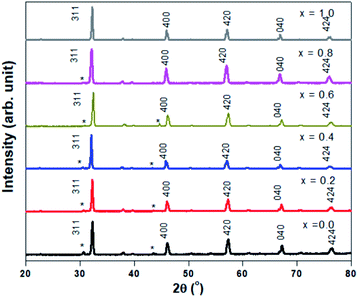 |
| | Fig. 1 XRD pattern of Sr2Ni1−xZnxTeO6 (x = 0.0, 0.2, 0.4, 0.6, 0.8, 1.0) with (*) labelled as Sr3TeO6. | |
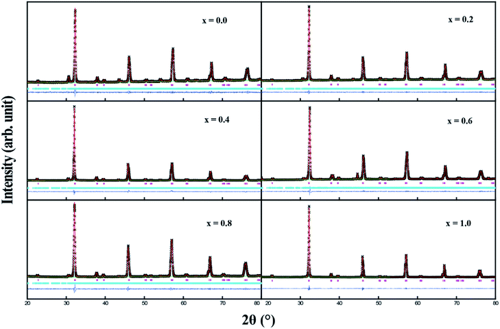 |
| | Fig. 2 Rietveld refinement of XRD pattern for Sr2Ni1−xZnxTeO6 (x = 0.0, 0.2, 0.4, 0.6, 0.8, 1.0). Black scattered symbols are observed data, the solid red line is the calculated pattern and the blue solid line is the difference. Pink and blue tick marks indicate the allowed Bragg reflections for primary and secondary phases, respectively. | |
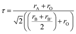
The lattice parameters for all compounds are presented in Table 1. Fig. 3 illustrates the octahedral structure that consists of Ni2+ and Te6+ as B and B′ cations, respectively, surrounded alternately by six O2− atoms whilst Sr2+ as A cations fill the occupancy between these NiTeO6 octahedral layers. Tolerance factor τ is used to predict the stability of the perovskite structure and given as eqn (1):
| |
 | (1) |
where
rA is the ionic radii of the A cation, which is Sr
2+ (1.44 Å);
rB and
rB′ are the ionic radii of B and B′ cations, which are Ni
2+/Zn
2+ (0.69 Å/0.74 Å) and Te
6+ (0.56 Å), respectively; and
rO is ionic radii of O
2− (1.40 Å). The
τ of the ideal crystal structure is 1. The value of
τ or Sr
2Ni
1−xZn
xTeO
6,
x = 0.0, 0.2, 0.4, 0.6, 0.8, 1.0 are 0.9844, 0.9893, 0.9869, 0.9844, 0.9820 and 0.9796, respectively, indicating ion distortion within all compounds as large size of Zn
2+ cation is doped in the compound. The average bond length of Ni/Zn–O for all compounds slightly changes with Zn concentration. Different average bond lengths in each compound cause the bond angles between octahedral B sites Ni/Zn–O–Te to increase from 158.6655° to 166.7800° for
x = 0.0 to
x = 1.0 due to a small change of octahedral structure distortion, which is related to
τ values without a structure change.
Table 1 Lattice parameters, unit cell volume, bond angles, bond lengths, fit goodness and tolerance factor (τ) in Sr2Ni1−xZnxTeO6 (x = 0.0, 0.2, 0.4, 0.6, 0.8 and 1.0) as obtained from Rietveld refinement and crystallite size from XRD characterisation
| Compounds |
x = 0.0 |
x = 0.2 |
x = 0.4 |
x = 0.6 |
x = 0.8 |
x = 1.0 |
| Lattice parameters |
| a (Å) |
5.6219(13) |
5.6272(9) |
5.6309(8) |
5.6078(10) |
5.6474(12) |
5.6527(6) |
| b (Å) |
5.5852(15) |
5.5903(10) |
5.5935(9) |
5.6451(8) |
5.6137(13) |
5.6196(8) |
| c (Å) |
7.8849(18) |
7.8912(12) |
7.8959(11) |
7.9157(11) |
7.9236(15) |
7.9343(8) |
| α |
90.000 |
90.000 |
90.000 |
90.000 |
90.000 |
90.000 |
| β |
90.018 |
90.063 |
90.046 |
90.111 |
90.141 |
90.063 |
| γ |
90.000 |
90.000 |
90.000 |
90.000 |
90.000 |
90.000 |
|
| Unit cell volume (Å3) |
| Unit cell volume, V |
247.580 |
248.241 |
248.692 |
250.580 |
251.199 |
252.042 |
|
| Bond length (Å) |
| 2× Ni/Zn–O1 |
2.1046(8) |
2.0523(4) |
2.0536(4) |
2.0582(3) |
2.0604(4) |
2.0636(2) |
| 4× Ni/Zn–O2 |
2.0472(6) |
2.0648(3) |
2.0661(3) |
2.0710(2) |
2.0726(3) |
2.0749(2) |
| <Ni/Zn–O> |
2.0759(7) |
2.0585(4) |
2.0598(4) |
2.0646(3) |
2.0665(4) |
2.0692(2) |
|
| Bond angle (°) |
| Ni/Zn–O1–Te |
161.5140(1) |
164.5530(0) |
164.5520(0) |
164.6530(0) |
164.5610(0) |
164.5670(0) |
| Ni/Zn–O2–Te |
155.8170(2) |
168.9990(0) |
168.9990(0) |
169.0000(0) |
168.9980(0) |
168.9930(0) |
| <Ni/Zn–O–Te> |
158.6655(2) |
166.7760(0) |
166.7760(0) |
166.8265 |
166.7795(0) |
166.7800(0) |
|
| Fit goodness |
| χ2 |
1.119 |
1.149 |
1.945 |
1.353 |
1.318 |
2.402 |
| RP (%) |
0.0310 |
0.0280 |
0.0325 |
0.0268 |
0.0351 |
0.0389 |
| RWP (%) |
0.0392 |
0.0361 |
0.0423 |
0.0366 |
0.0446 |
0.0513 |
| τ |
0.9844 |
0.9893 |
0.9869 |
0.9844 |
0.9820 |
0.9796 |
|
| Crystalline size (nm) |
| Crystalline size (D) |
30.6307 |
29.7252 |
30.6268 |
34.7859 |
22.5119 |
36.0399 |
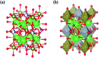 |
| | Fig. 3 (a) The crystal structure for Sr2Ni1−xZnxTeO6 (x = 0.0, 0.2, 0.4, 0.6, 0.8 and 1.0). Sr represent as green-colored balls, Ni represent as grey-colored balls, Zn represent as blue balls and O represent as red-colored balls. (b) Structure of SrNi1−xZnxTeO6 (x = 0.0, 0.2, 0.4, 0.6, 0.8 and 1.0), where the Sr are 12-fold coordinated and Ni and Zn is 6-fold coordinated with the polyhedral. | |
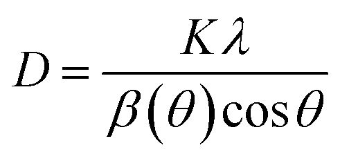
The Scherrer equation shown in eqn (2) is used to calculate the crystalline size (D):
| |
 | (2) |
where
K is a constant with 0.94;
λ is the wavelength of XRD, which is 0.1541 nm for Cu-K
α radiation;
β(
θ) is the full width at half maximum in radians; and
θ is the angle of the most intense peak in XRD. The
D values for Sr
2Ni
1−xZn
xTeO
6,
x = 0.0, 0.2, 0.4, 0.6, 0.8, 1.0 are 30.6307, 29.7252, 30.6268, 34.7859, 22.5119 and 36.0399 nm, respectively, as listed in
Table 1. The increase in crystalline size from 29.7252 nm for
x = 0.2 to 34.7859 nm for
x = 0.6 represents that Zn
2+ dopant provides the better crystallisation as doping concentrations increase. The crystalline size of the compound is comparable with other Te-based double perovskites, SrLaLiTeMnO
6 and SrLaLiNdTeO
6, in range of 20–29 and 28–42 nm, respectively.
6,18
Morphology
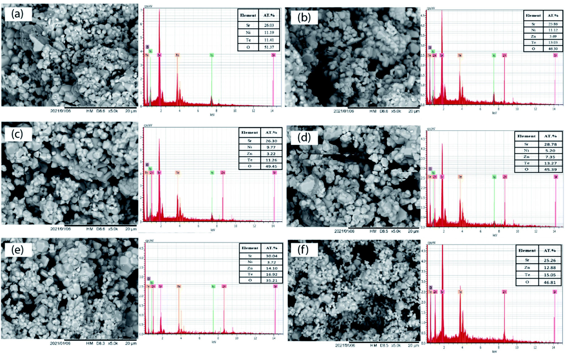
The SEM images of the Sr2Ni1−xZnxTeO6 (x = 0.0, 0.2, 0.4, 0.6, 0.8, 1.0) series are illustrated in Fig. 4. The morphologies of the samples obtained from the SEM images reveal that the surface of the samples are almost identical and moderately homogenous. Moreover, in all samples, the size of the particles is large, and they are aggregated in groups due to the higher preparation temperature; the same effect of temperature was observed in the morphology analysis by Lan et al. and Alsabah et al. with series of La2NiMnO6 and BaSrZnWO6, respectively.12,19 Each sample has grain of various sizes, 1.53–1.67 μm for Sr2NiTeO6, 2.50–2.99 μm for Sr2Ni0.8Zn0.2TeO6, 2.02–2.49 μm for Sr2Ni0.6Zn0.4TeO6, 1.88–2.03 μm for Sr2Ni0.4Zn0.6TeO6, 1.23–1.38 μm for Sr2Ni0.2Zn0.8TeO6 and 1.20–1.38 μm for Sr2ZnTeO6. EDX analysis was performed with all samples using the SEM images. All EDX results presented in Fig. 4 indicate the percentage elemental composition of Sr, Ni, Zn, Te and O. The atomic percentage of Ni in pristine sample (x = 0.0) is 11.19%, which decreases as the doping content increases and becomes 3.72% (x = 0.8) and none at x = 1.0. It shows that Zn has been incorporated at the Ni site in the crystal lattice. The atomic percentages of constituent elements are tabulated in the inset of Fig. 4. The values of atomic percentage for each samples are nearly equal to the ratios of the element during sample preparation.
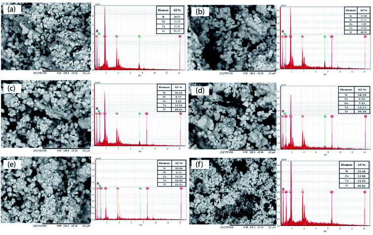 |
| | Fig. 4 Microstructures and EDX patterns of Sr2Ni1−xZnxTeO6 (a) x = 0.0, (b) x = 0.2, (c) x = 0.4, (d) x = 0.6, (e) x = 0.8 and (f) x = 1.0. | |
FTIR spectroscopy
The FTIR spectra were used to identify the phase formation of the perovskite. For Sr2Ni1−xZnxTeO6 double perovskite, the FTIR spectra of the series are similar and show a very simple spectra pattern, as usually found in perovskite materials.20–22 The spectra revealed two distinctive absorption bands between 700–450 cm−1 region, as depicted in Fig. 5. The high-energy, strong band observed at around 660 cm−1 corresponded to the antisymmetric stretching mode of Ni–O6, Zn–O6 and Te–O6 octahedral due to the higher charge of the Ni2+, Zn2+ and Te4+ cations.23 The bands that appeared around 550 cm−1 are suggested due to deformational modes of Ni–O6, Zn–O6 and Te–O6 octahedrals. Fig. 5 shows the transmittance of the Sr2Ni1−xZnxTeO6 double-perovskite series versus wave number, and all the samples confirm the molecular bands on the perovskite oxide structure.
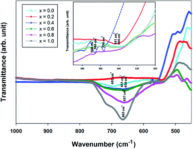 |
| | Fig. 5 FTIR spectra of Sr2Ni1−xZnxTeO6 (x = 0.0, 0.2, 0.4, 0.6, 0.8 and 1.0). | |
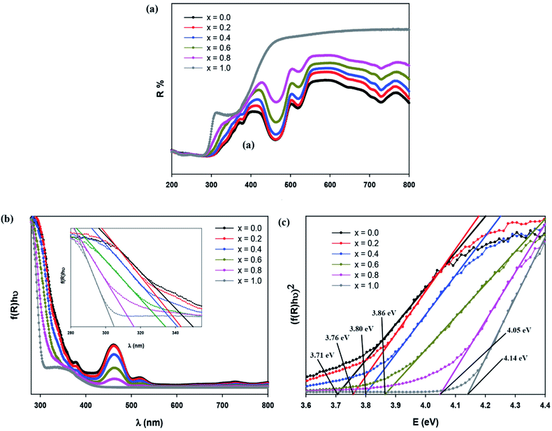
UV-visible diffuse reflectance spectroscopy
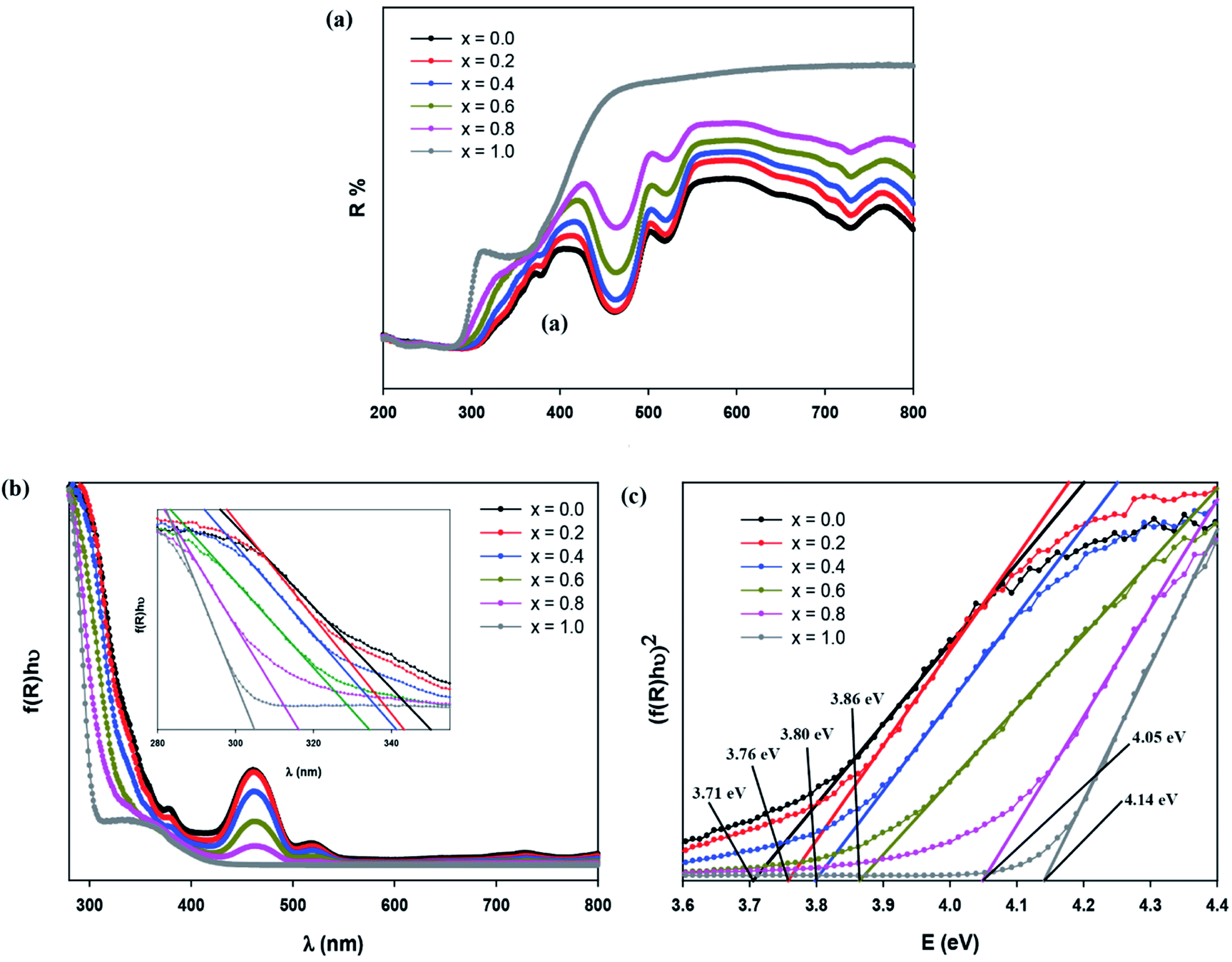
Fig. 6(a) displays the diffuse reflectance spectrum of Sr2Ni1−xZnxTeO6 (x = 0.0, 0.2, 0.4, 0.6, 0.8, 1.0) in the range of 200–800 nm wavelength at 298 K. The intensity of peaks increases as the Zn content increases. A strong absorption band at 300 nm to 450 nm may be related to the charge transfer transition between doped Zn2+ and O2− (valence and conduction band) in the lattice structure.18,24 As Zn2+ increases, the increase of reflectance value of compound shows the reduction of absorbance properties. The absorption coefficient is calculated from diffuse reflectance spectra using Kubelka–Munk (KM) function, as shown in eqn (3):12| |
 | (3) |
where f(R) represents the KM function, α is the absorption coefficient, s is the scattering coefficient and R is the reflection coefficient. The relation between absorbance (f(R)hν) and wavelength is plotted in Fig. 6(b). By taking the intercept of the extrapolations to zero absorption with the photon energy axis, the absorption edge value can be obtained. The bandgap energy value, Eg, can be calculated by applying the following equation:| |
 | (4) |
where λ represents the absorption edge wavelength. The band gap energy can be obtained directly from the x intersection of Tauc plot fitting, as illustrated in Fig. 6(c), corresponding to Tauc eqn (5):| | |
[f(R)hν]n = A(hν − Eg)
| (5) |
where hν is the incident photon energy, Eg represents the band gap energy and n is the constant values of 0.5, 2, 1.5 and 3 for direct allowed, indirect allowed, direct forbidden and indirect forbidden transition, respectively.6,24,25 This plot shows that the value of n is 0.5, and the curve has a linear part of. Therefore, the compounds are classified as direct band gap semiconductor, whose top of the valence band and bottom of the conduction band occur at the same value of momentum. Table 2 shows that Eg according to the KM and Tauc plot are comparable with each other. In addition, the increase in optical band gap energy value is related to the increase in Zn concentration in compound. Eng et al. reported that the decrease in the ionic radii of B′ site ions. In addition, the study reported that when the bond angle becomes less than 180° with octahedral tilting, an increase in bandgap is observed due to the narrowing of conduction band.26 Zn-doped possesses high bandgap value than for Sr2NiTeO6 because the ionic radii for Ni2+ and Zn2+ are 2.09 and 2.14 Å, respectively.
 |
| | Fig. 6 (a) Diffuse reflectance spectrum, (b) Absorbance as a function of wavelength (Kubelka–Munk) plot compounds, (c) Tauc plot of Sr2Ni1−xZnxTeO6 (x = 0.0, 0.2, 0.4, 0.6, 0.8 and 1.0) double perovskite compounds. | |
Table 2 Band gap energy according to the Kubelka–Munk and Tauc plot for direct transition Sr2Ni1−xZnxTeO6 (x = 0.0, 0.2, 0.4, 0.6, 0.8 and 1.0)
| Band gap energy |
x = 0.0 |
x = 0.2 |
x = 0.4 |
x = 0.6 |
x = 0.8 |
x = 1.0 |
| Cut-off wavelength (±0.01 nm) |
350.08 |
343.26 |
341.29 |
334.39 |
316.20 |
304.87 |
| Eg by cutoff wavelength (±0.01 nm) |
3.54 |
3.61 |
3.63 |
3.71 |
3.92 |
4.07 |
| Eg by Tauc plot (±0.01 nm) |
3.71 |
3.76 |
3.80 |
3.86 |
4.05 |
4.14 |
Impedance spectroscopy analysis
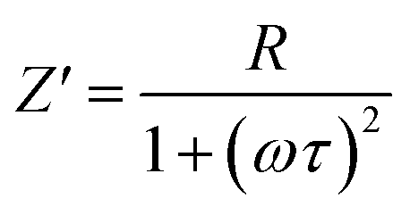
To distinguish between bulk and grain boundary effect, relaxation phenomena and polarisation effect within the materials, the impedance spectroscopy (IS) method was employed from the output response of input ac signal applied across the pellet sample. The measured complex impedance (Z) has real (Z′) and imaginary (Z′′) components, which are interpreted as eqn (6)–(8):| |
 | (7) |
| |
 | (8) |
where R is the resistance of the sample, ω is the angular frequency and τ is the relaxation time (RC). τ is calculated by an expression τ = RgCg, where Rg and Cg are the grain resistance and grain capacitance, respectively, which are arranged in parallel circuit. These parameters are obtained from Zview software and provided in Table 3.
Table 3 Grain resistance, Rg and grain capacitance, Cg of SrNi1−xZnxTeO6 (x = 0.0, 0.2, 0.4, 0.6, 0.8 and 1.0) as obtained from Cole–Cole plot fitting with R-CPE equivalent circuit model
| x |
Grain resistance, Rg (108 Ω) |
Grain capacitance, Cg (10−11 F) |
| 0.0 |
2.097 |
9.380 |
| 0.2 |
1.925 |
6.638 |
| 0.4 |
1.099 |
5.768 |
| 0.6 |
1.002 |
4.972 |
| 0.8 |
1.012 |
7.853 |
| 1.0 |
1.336 |
10.879 |
The complex impedance measurement of the Sr2Ni1−xZnxTeO6 (x = 0.0, 0.2, 0.4, 0.6, 0.8, 1.0) double perovskite compounds were conducted from 1 Hz to 0.1 MHz in the temperature of 298 K. Fig. 7(a) depicts the variation of real part of impedance (Z′) with frequency. Z′ for all samples are stable up to low frequency (∼100 Hz) and reduces with the increase in frequency. The reduction of Z′ values indicates an increase in AC conductivity as the frequency increases.27,28 At nearly about 90 Hz frequency, all curves of Z′ start to merge, revealing that the liberation of space charges causes the increase in AC conductivity in the compound.29 Fig. 7(b) illustrates the variation of imaginary part of impedance (Z′′) with frequency at a temperature of 298 K. A single peak present in the graph indicates the presence of one dielectric relaxation within the double-perovskite materials. The dominant relaxation involved is due to interface effect. The considerable decrease in  and
and  values for rich codoping Zn compositions might be due to the decrease in grain resistance (Rg). These results suggest that doping of Zn into the Sr2NiTeO6 remarkably affect the electrical microstructure. Suman Rani et al. reported that the electrical microstructure properties of doped compositions substantially change with the increase in Zn concentration in perovskite lattice.30
 |
| | Fig. 7 (a) Variation of Z′ and (b) Z′′ with frequency for SrNi1−xZnxTeO6 (x = 0.0, 0.2, 0.4, 0.6, 0.8 and 1.0) at temperature 298 K. | |
The Cole–Cole plot is presented by semicircle arcs. In this case, the plot only consists of a single semicircle arc, indicating a single phase contribution to the electrical behaviour within the sample. The fitting of the experiment data was carried out by using Zview software. The circuit used to fit the results is shown as an inset to Fig. 8. The circuit used to fit the semicircle arc consists of a single RC circuit, which represents the interface of the material.31 The constant phase element was used in circuit instead of capacitance to accommodate nonideal capacitive behaviour due to the inhomogeneous interface. The scattered symbols in Fig. 8 indicate experimental data, whereas the solid green lines show the fitted results obtained from circuit used by Zview software. Debye stated that a perfect Debye type relaxation phenomenon shows the centre of the semicircles coincide with the real impedance axis. Thus, the Cole–Cole plot of all compounds in Fig. 8 disobey the Debye type of relaxation phenomena due to the imperfection of the sample.32 The obtained parameters from the fitting are listed in Table 3 for all samples. The decrease of grain resistance (Rg) as Zn concentration increases has been discussed in the previous section. The values of capacitance in the range of 10−11 F are correlated with the interface or grain boundary, suggesting the presence of interface effects in the samples.28
 |
| | Fig. 8 Cole–Cole plots for Sr2Ni1−xZnxTeO6 (x = 0.0, 0.2, 0.4, 0.6, 0.8 and 1.0). | |
Dielectric study
The dielectric analysis of the compound can be explained by the complex permittivity having real and imaginary parts, as shown in eqn (9)–(11):| | |
ε*(ω) = ε′(ω) + jε′′(ω)
| (9) |
| |
 | (10) |
| |
 | (11) |
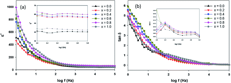
where ε′(ω) is the dielectric constant as a function of angular frequency (ω), which indicates the energy stored, and ε′′(ω) is the energy loss during every cycle of electric field. Z′ and Z′′ are real and imaginary components of impedance, respectively. ε0 is the absolute permittivity (8.85 × 10⁻¹² C2 N−1 m−1), and G is the area of electrode per thickness of pellet sample. Dependency of ε′ and ε′′ with frequency are correlated with various polarisation effects – ionic, dipolar, electronic and space charge that appears at multiple levels of material reaction due to short and long-range movement of mobile charges.33 The real component of dielectric (ε′) indicates the ability of the electrical dipoles within the sample to align with the external electric field, whereas imaginary component of dielectric (ε′′) indicates the energy dissipation in the compound. The frequency dependence of dielectric constant, ε′, and tangent loss, tanδ, of the Sr2Ni1−xZnxTeO6 compounds between range of 1 Hz to 0.1 MHz at room temperature are shown in Fig. 9(a) and (b), respectively. All samples show a trend similar to normal dielectric materials. At a low frequency (∼1 Hz), the dielectric values are the highest for all samples because the dipoles within the samples align themselves along the applied electric field and contribute fully the total polarisation of dielectric. The high values of ε′ unexpectedly observed only at very low frequencies may be attributed to the fact that the free charges build up at interfaces within the bulk of the sample (interfacial Maxwell–Wagner polarisation) and at the interface between the sample, and the electrode space-change polarisation31 between these compounds reveal that Sr2Ni0.2Zn0.8TeO6 has the highest dielectric value (991.9 ± 0.1) and dielectric loss (5.9 ± 0.1) at 1 Hz.
 |
| | Fig. 9 (a) Frequency dependence of ε′ and (b) tanδ for Sr2Ni1−xZnxTeO6 (x = 0.0, 0.2, 0.4, 0.6, 0.8 and 1.0) at 298 K (inset represents the zoom view of frequency range from 104 Hz to 105 Hz). | |
These results suggest that codoping of Zn into the Sr2NiTeO6 may be attributed to the low grain resistance, which allows the charge carriers to respond to an electric field, as listed in Table 3.30 In addition, the dependency of frequency and dielectric constant show milder decrease for Sr2NiTeO6 and Sr2Ni0.8Zn0.2TeO6, representing its better perspective for electronic applications.33 At a high frequency (∼100 Hz), the variation in the field is very rapid for the electrical dipoles and unable to realign themselves. Hence, dielectric permittivity can become negligible, resulting in the decrease of dielectric constant ε′ with increasing frequency. The values of bulk density, dielectric constant and dielectric loss for each samples are tabulated in Table 4. At 0.1 MHz, the Sr2Ni0.4Zn0.6TeO6 and Sr2Ni0.2Zn0.8TeO6 have the greatest ε′ (59.9 ± 0.1). The highest density of Sr2Ni0.2Zn0.8TeO6 could explain its higher dielectric value at both regions compared with other compounds.18
Table 4 Bulk density, ρ, dielectric constant ε′ and dielectric loss tanδ at 0.1 MHz of SrNi1−xZnxTeO6 (x = 0.0, 0.2, 0.4, 0.6, 0.8 and 1.0)
| x |
Bulk density, ρ (g cm−1) |
Dielectric constant, ε′ at 0.1 MHz |
Dielectric loss, tanδ at 0.1 MHz |
| 0.0 |
5.701 |
40.2 |
0.04 |
| 0.2 |
5.818 |
56.4 |
0.04 |
| 0.4 |
5.894 |
57.3 |
0.05 |
| 0.6 |
5.937 |
59.9 |
0.04 |
| 0.8 |
6.008 |
59.9 |
0.05 |
| 1.0 |
5.818 |
42.2 |
0.05 |
Conclusions
In this paper, the structural and dielectric properties of polycrystalline Sr2Ni1−xZnxTeO6 (x = 0.0, 0.2, 0.4, 0.6, 0.8, 1.0) were synthesised using a conventional solid-state reaction method. The sample was crystallised into a I2/m monoclinic space group. SEM images revealed that the grain sizes decrease as Zn content increases, and the samples are aggregated in groups. The absorption band obtained from FTIR spectra showed that all the samples confirm the molecular bands on the perovskite oxide structure. The UV-vis analysis showed that Eg increases with increase in Zn content. The IS results confirmed that the nonDebye type of relaxation phenomena occurred for all samples. The EIS characterisation revealed that Sr2Ni0.2Zn0.8TeO6 double-perovskite compounds have high dielectric constants (∼1000 at 1 Hz and ∼60 at 105 Hz) and exhibit low dielectric loss (tanδ ≤ 0.20) in the range of 104–105 Hz frequency at room temperature. This study shows that the dielectric properties of Sr2Ni1−xZnxTeO6 can be altered by codoping method. These materials could be promising candidates for use in electronic devices because they possess dielectric behaviour.
Author contributions
F. I. H Alias carried out the lab work, heavily participated in data analysis, drafted the manuscript; Dr R. Rajmi participated in data analysis; M. F. Maulud and Dr Z. Mohamed revised the manuscript. All authors have read and agreed to the published version of the manuscript.
Conflicts of interest
There are no conflicts to declare.
Acknowledgements
The authors would like to thanks the Centre of Nanoscience and Nanotechnology, Universiti Teknologi MARA (UiTM) for UV-vis spectroscopy. This work was financially supported by the Ministry of Higher Education (MOHE) and Universiti Teknologi MARA (UiTM) through the Fundamental Research Grant Scheme (600-IRMI/FRGS 5/3 (356/2019)).
Notes and references
- A. A. Allah, M. Elhadi and O. A. Yassien, Adv. Mater. Res., 2013, 717, 133–138 Search PubMed.
- A. Zaraq, B. Orayech, J. M. Igartua and A. El Bouari, Powder Diffr., 2013, 6, 1–11 Search PubMed.
- A. Dias, G. Subodh, M. T. Sebastian, M. M. Lage and R. L. Moreira, Chem. Mater., 2008, 20, 4347–4355 CrossRef CAS.
- A. Dias, G. Subodh, M. T. Sebastian and R. L. Moreira, J. Raman Spectrosc., 2010, 41, 702–706 CrossRef CAS.
- R. Ubic, S. Letourneau, S. Thomas, G. Subodh and M. T. Sebastian, Chem. Mater., 2010, 22, 4572–4578 CrossRef CAS.
- M. Z. M. Halizan, Z. Mohamed and A. K. Yahya, Mater. Res. Express, 2020, 7, 086301 CrossRef CAS.
- F. Zhao, Z. Yue, Z. Gui and L. I. Longtu, Jpn. J. Appl. Phys., Part 1, 2005, 44, 8066–8070 CrossRef CAS.
- V. L. Vilesh and G. Subodh, Ceram. Int., 2018, 44, 12036–12041 CrossRef CAS.
- M. Z. M. Halizan, A. K. Yahya, N. B. Ibrahim, N. Ibrahim and Z. Mohamed, Digest Journal of Nanomaterials and Biostructures, 2020, 15, 733–741 Search PubMed.
- K. I. Kobayashi, T. Kimura, H. Sawada, K. Terakura and Y. Tokura, Nature, 1998, 395, 677–680 CrossRef CAS.
- M. Itoh, I. Ohta and Y. Inaguma, Mater. Sci. Eng., B, 1996, 41, 55–58 CrossRef.
- Y. A. Alsabah, M. S. AlSalhi, A. A. Elbadawi and E. M. Mustafa, Materials, 2017, 10, 1–12 CrossRef PubMed.
- K. Ramesh Kumar, N. Harish Kumar, G. Markandeyulu, J. A. Chelvane, V. Neu and P. D. Babu, J. Magn. Magn. Mater., 2008, 320, 2737–2740 CrossRef.
- W. Yansen, D. Kim, K. J. Parwanta, C. Liu and B. W. Lee, Curr. Appl. Phys., 2015, 15, 120–123 CrossRef.
- F. I. H. Alias, M. F. Maulud and Z. Mohamed, AIP Conf. Proc., 2021, 1, 030001 CrossRef.
- B. Orayech, L. Ortega-San-Martín, I. Urcelay-Olabarria, L. Lezama, T. Rojo, M. I. Arriortua and J. M. Igartua, Dalton Trans., 2016, 45, 14378–14393 RSC.
- D. D. Han, W. Gao, N. N. Li, R. L. Tang, H. Li, Y. M. Ma, Q. L. Cui, P. W. Zhu and X. Wang, Chin. Phys. B, 2013, 22, 059101 CrossRef.
- M. Z. M. Halizan, Z. Mohamed and A. K. Yahya, Sci. Rep., 2021, 11, 1–13 CrossRef PubMed.
- C. Lan, S. Zhao, T. Xu, J. Ma, S. Hayase and T. Ma, J. Alloys Compd., 2016, 655, 208–214 CrossRef CAS.
- G. Blasse and A. F. Corsmit, J. Solid State Chem., 1973, 6, 513–518 CrossRef CAS.
- M. Gateshki, J. M. Igartua and E. Hernández-Bocanegra, J. Phys.: Condens. Matter, 2003, 15, 6199–6217 CrossRef CAS.
- M. Z. M. Halizan, Z. Mohamed and A. K. Yahya, AIP Conf. Proc., 2021, 1, 030005 CrossRef.
- Y. A. Alsabah, A. A. Elbadawi, E. M. Mustafa and M. A. Siddig, J. Mater. Sci. Chem. Eng., 2016, 04, 61–70 CAS.
- Y. A. Alsabah, M. S. AlSalhi, E. M. Mustafa, A. A. Elbadawi, S. Devanesan and M. A. Siddig, Crystals, 2020, 10, 299 CrossRef CAS.
- N. A. F. M. Saadon, N. M. Ali, N. Ibrahim and Z. Mohamed, AIP Conf. Proc., 2021, 1, 030006 CrossRef.
- H. W. Eng, P. W. Barnes, B. M. Auer and P. M. Woodward, J. Solid State Chem., 2003, 175, 94–109 CrossRef CAS.
- B. N. Parida, N. Panda, R. Padhee, P. R. Das and R. N. P. Choudhary, J. Mater. Sci.: Mater. Electron., 2017, 28, 1824–1831 CrossRef CAS.
- Z. Imran, M. A. Rafiq and M. M. Hasan, AIP Adv., 2014, 4, 13 Search PubMed.
- R. Das and R. N. P. Choudhary, J. Mater. Sci.: Mater. Electron., 2018, 29, 19099–19110 CrossRef CAS.
- S. Rani, N. Ahlawat, R. Punia, K. M. Sangwan and P. Khandelwal, Ceram. Int., 2018, 44, 23125–23136 CrossRef CAS.
- D. K. Mahato, A. Dutta and T. P. Sinha, Bull. Mater. Sci., 2011, 34, 455–462 CrossRef CAS.
- R. Das and R. N. P. Choudhary, J. Adv. Ceram., 2019, 8, 174–185 CrossRef CAS.
- J. Bijelić, D. Tatar, S. Hajra, M. Sahu, S. J. Kim, Z. Jagličić and I. Djerdj, Molecules, 2020, 25, 3996 CrossRef PubMed.
|
| This journal is © The Royal Society of Chemistry 2021 |

 Open Access Article
 This Open Access Article is licensed under a Creative Commons Attribution-Non Commercial 3.0 Unported Licence
 a,
Rozilah Rajmib,
Mohd Fauzi Mauluda and
Zakiah Mohamed
a,
Rozilah Rajmib,
Mohd Fauzi Mauluda and
Zakiah Mohamed


 and
and  values for rich codoping Zn compositions might be due to the decrease in grain resistance (Rg). These results suggest that doping of Zn into the Sr2NiTeO6 remarkably affect the electrical microstructure. Suman Rani et al. reported that the electrical microstructure properties of doped compositions substantially change with the increase in Zn concentration in perovskite lattice.30


