
 Open Access Article
 This Open Access Article is licensed under a
 Creative Commons Attribution 3.0 Unported Licence
Air stable and highly efficient Bi3+-doped Cs2SnCl6 for blue light-emitting diodes†
Yue Yao‡
ab,
Si-Wei Zhang‡ a,
Zijian Liuab,
Chun-Yun Wang*ab,
Ping Liuab,
Lan Ma*b,
Guodan Wei*ab and
Feiyu Kangab
a,
Zijian Liuab,
Chun-Yun Wang*ab,
Ping Liuab,
Lan Ma*b,
Guodan Wei*ab and
Feiyu Kangab
aTsinghua-Berkeley Shenzhen Institute (TBSI), Tsinghua University, Shenzhen, 518055, China. E-mail: wangcy0317@gmail.com; malan@sz.tsinghua.edu.cn; weiguodan@sz.tsinghua.edu.cn
bTsinghua Shenzhen International Graduate School, Tsinghua University, Shenzhen, 518055, China
First published on 2nd August 2021
Abstract
Cs2SnCl6 perovskite has recently attracted attention as a promising optoelectronic material owing to its better stability and reduced toxicity than its lead counterparts. However, its luminescence performance hardly satisfies the requirements. Hence, a series of Bi3+-doped Cs2SnCl6 (Cs2SnCl6:Bi3+) with enhanced luminescence were synthesized by a solution-phase route. The results show that the initial concentration of Sn2+ can adjust the nucleation density and the quality of the crystal nucleus growth, which will affect the Bi3+ doping amount, crystal morphology, and photophysical properties of Cs2SnCl6:Bi3+. Cs2SnCl6:Bi3+ shows excellent stability in the atmosphere with a photoluminescence (PL) of around 456 nm and a photoluminescence quantum yield (PLQY) of 31%. The luminescence performance results from [BiSn4+3+ + VCl] defects caused by the Bi3+ doping. The blue LED based on the Cs2SnCl6:Bi3+ phosphor exhibits a long life of about 120 h and a Commission Internationale de L'Eclairage (CIE) color coordinates of (0.14, 0.11). This work demonstrates a strategy for Bi-doped perovskites with good stability. This investigation will facilitate the development of Cs2SnCl6:Bi3+ for blue LED applications.
Lead halide perovskites have been extensively studied for their excellent performance in photovoltaics, light-emitting diodes (LEDs), and photodetectors. However, the toxic lead and dissatisfied stability of the lead halide perovskites suppress their practical applications, particularly the high solubility of Pb2+ in water, severely threatening the biological system and human health. Therefore, non-toxic Sn-based perovskites could be an ideal alternative.1,2 Sn2+-based CsSnCl3 barely shows any optoelectronic application due to its low PLQY, oxidation, and humidity,3 while Sn4+-based Cs2SnCl6 exhibits high anti-oxidation stability along with promising optoelectronic properties.1 Cs2SnCl6 has a vacancy-ordered double perovskite structure with isolated [SnCl6]4− octahedra, improving the photoluminescence by quantum confinement effect.4
Several strategies have been reported to enhance the photoluminescence of Cs2SnCl6, and impurity doping has been demonstrated to be a facile and effective method.2,4,5 The defects in doped Cs2SnCl6 cause a charge imbalance, which must be rectified by the localization of electrons and holes or by the generation of impurity states within the bandgap, and this would add the localized level and affect luminescence properties.6 Numerous types of heteroatoms have been employed. Ce3+-doped Cs2SnCl6 could tune the [CeSn4+3+ + VCl] defect density with different Ce3+ concentrations, affecting the crystal emission and exhibiting an achievable PLQY of 6.54%.2 Bi3+-doped Cs2SnCl6 (Cs2SnCl6:Bi3+) exhibited a higher PLQY of around 80% due to the hetero-valent replacement of Sn4+ by Bi3+ and exhibited a bandgap of about 3.05 eV,4 which was aspirational for the blue emitter. The defect density can also be affected by the doping process such as annealing temperature, subsequently changing the emission properties.5 The excellent Cs2SnCl6:Bi3+ shows great potential for practical applications. Cs2SnCl6 originates from Sn4+, but previous studies certified that only Sn4+ could not achieve the abundant doping of Bi3+. Although abundant studies have been carried out, the precursor concentration effects of Sn2+ and Sn4+ on the Bi3+ doping are still unknown, and the changes in morphology and photophysical properties caused by the doping process still need to be systematically reported. Simultaneously, the application of Cs2SnCl6:Bi3+ in LED devices, particularly the device stability, still needs more study.
In this study, Cs2SnCl6:Bi3+ was synthesized by a solution-phase route with varied precursor concentrations. The nucleation density and the quality of crystal nucleus growth can be tuned by the initial Sn2+ concentration, which can affect the crystal morphology, Bi3+ doping amount, and the photophysical properties of Cs2SnCl6:Bi3+. The nucleus growth process is accompanied by [BiSn4+3+ + VCl] formation, which enhanced the luminescence intensity and extended the exciton delay time. The adjusted sample shows a PL peak of around 456 nm, PLQY of 31%, and good stability. More importantly, the blue LED based on Cs2SnCl6:Bi3+ phosphor exhibits a blue emission at the CIE coordinates of (0.14, 0.11), an external quantum efficiency (EQE) of 6.24%, and a luminescence power of 4.6 lm W−1. The device can continue to work for 120 h with blue luminescence.
The synthesis process of Cs2SnCl6 is shown in ESI.† In brief, two stages occurred as shown below. Sn2+ instead of Sn4+ was selected as the Sn precursor. By changing the amount of HCl added, the precursor solution's concentration (refers to the initial Sn2+ concentration) can be adjusted, affecting the nucleation density and quality of the crystal nucleus growth, then the morphology and photophysical properties of the product.
Stage 1: the nucleation process
| SnCl2 + 2HCl + O2 → SnCl4↓ + H2O |
| SnCl2 + 2HCl → H[SnCl3] |
| SnCl4 + 2HCl → H2[SnCl6] |
| H2[SnCl6] + 2CsCl → Cs2SnCl6↓ + 2HCl |
| H[SnCl3] + CsCl → CsSnCl3↓ + HCl |
Stage 2: the oxidation of CsSnCl3 and the further growth of Cs2SnCl6
| CsSnCl3 → CsCl + SnCl2 |
| SnCl2 + 2HCl + O2 → SnCl4↓ + H2O |
| SnCl4 + 2HCl → H2[SnCl6] |
| H2[SnCl6] + 2CsCl → Cs2SnCl6↓ + 2HCl |
It can be concluded that Cs2SnCl6 originates from Sn4+, but previous studies certified that only Sn4+ cannot achieve the doping of Bi3+.4 Therefore, an Sn4+-poor/Sn2+-rich mixture was employed to facilitate the incorporation of Bi3+ into Cs2SnCl6. Therefore, SnCl2 was used as the precursor. It is still unclear at which step Bi3+ is doped. With the adjustment in the amount of HCl added, the concentration of Sn2+ in the precursor and Sn4+ produced in the reaction process can influence the Bi3+ doping. The amount and concentration of each reactant are listed in Table S1.† Monoclinic CsSnCl3 is observed when the precursor concentration of Sn2+ is too high (higher than 0.143 mol L−1), as shown in Fig. S1.† The monoclinic CsSnCl3 would significantly suppress luminescence and hinder Bi3+ doping. Consequently, the concentrations of the precursor of Sn2+ were investigated as 0.143, 0.125, 0.111, 0.100, and 0.091 mol L−1.
The scanning electron microscopy (SEM) images in Fig. 1 show the effects of the precursor concentration on the morphology of the Bi3+-doped Cs2SnCl6 (Cs2SnCl6:Bi3+) perovskite. The particles agglomerated to reduce the inherently high surface energy with a particle size less than 10 μm featuring phosphors' characteristics.7 Numerous small quasi-spherical particles adhered to the particles with high crystallinity, indicating that the crystal growth process is similar. The formation process of Cs2SnCl6 includes two stages: (1) the nucleation process of the initial Cs2SnCl6 and CsSnCl3 crystals and (2) the further growth of Cs2SnCl6 along with the oxidation of CsSnCl3. Both processes were related to the concentration of the initial reactants.
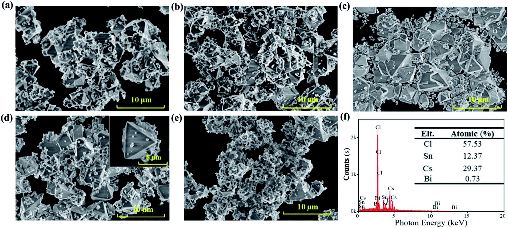 | ||
| Fig. 1 SEM images of Cs2SnCl6:Bi3+ synthesized at different precursor concentrations: (a) 0.143 mol L−1; (b) 0.125 mol L−1; (c) 0.111 mol L−1; (d) 0.100 mol L−1; (e) 0.091 mol L−1. (f) EDS results of Cs2SnCl6:Bi3+ obtained at 0.100 mol L−1. | ||
High concentration of Sn2+ precursors (0.143 mol L−1 and 0.125 mol L−1) led to the abundant and dense nucleation of the initial Cs2SnCl6 and CsSnCl3 crystals in the first stage, consuming a considerable number of initial reactants. Therefore, there were not enough reactants for the continuation of the crystal growth, leading to some particles being agglomerated together without total growth (Fig. 1(a) and (b)). As the concentration decreased (0.111 mol L−1, 0.100 mol L−1), the nucleation of the initial Cs2SnCl6 and CsSnCl3 crystals decreased, and the crystals could grow fully. Fig. 1(c) and (d) show more large particles with good crystalline and clean surfaces, and the inset image of Fig. 1(d) shows the details of Cs2SnCl6 tetrahedral with thin particles. When the concentration decreased to 0.091 mol L−1, the second stage was severely suppressed due to the overdispersed nucleus. As a result, Fig. 1(e) shows only some small quasi-spherical particles with an insufficient crystal growth. Small-sized particles possessed higher chemical potentials, solubility and surface energy, which may not help improve the stability of Cs2SnCl6:Bi3+. Therefore, it can be concluded that the sample in Fig. 1(d) can exhibit higher stability. Further, the EDS of the sample at a concentration of 0.100 mol L−1 was characterized (Fig. 1(f)). 0.73% atomic Bi3+ was doped into the host material Cs2SnCl6, and the Bi3+-doped Cs2SnCl6 (Cs2SnCl6:Bi3+) was obtained.
The crystal structure properties of Cs2SnCl6:Bi3+ synthesized at different precursor concentrations are shown in Fig. 2(a). All of the XRD patterns are indexed to the Cs2SnCl6 phase (ICSD 29030, Fm![[3 with combining macron]](https://www.rsc.org/images/entities/char_0033_0304.gif) m, a = 10.369 Å),8 and no impurity phases can be observed, indicating its highly crystalline nature. However, the diffraction peaks show relatively small deviations when compared to that of the standard Cs2SnCl6 phase. The Rietveld refinement results show an enlargement of the lattice parameter within 0.41% for all the doped Cs2SnCl6 (Table 1 and Fig. S2†), which is ascribed to the different sizes between Bi3+ (1.01 Å) and Sn4+ (0.71 Å).9 More specifically, the strongest diffraction peaks that oriented towards the (220) direction demonstrate a left shift, as shown in the inset of Fig. 2(a), which implied the formation of chlorine vacancies [BiSn4+3+ + VCl] when the Bi3+ cations randomly substituted Sn4+ cations.2,4,5
m, a = 10.369 Å),8 and no impurity phases can be observed, indicating its highly crystalline nature. However, the diffraction peaks show relatively small deviations when compared to that of the standard Cs2SnCl6 phase. The Rietveld refinement results show an enlargement of the lattice parameter within 0.41% for all the doped Cs2SnCl6 (Table 1 and Fig. S2†), which is ascribed to the different sizes between Bi3+ (1.01 Å) and Sn4+ (0.71 Å).9 More specifically, the strongest diffraction peaks that oriented towards the (220) direction demonstrate a left shift, as shown in the inset of Fig. 2(a), which implied the formation of chlorine vacancies [BiSn4+3+ + VCl] when the Bi3+ cations randomly substituted Sn4+ cations.2,4,5
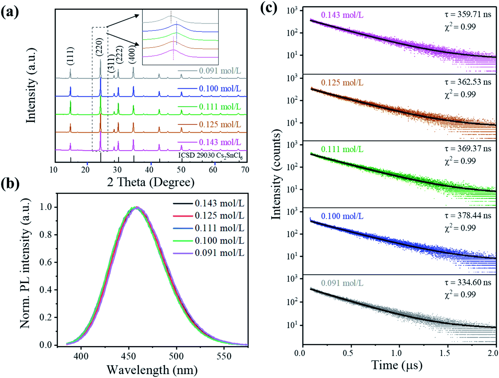 | ||
| Fig. 2 Structure and luminescence properties of Cs2SnCl6:Bi3+ synthesized at different precursor concentrations: (a) room-temperature XRD patterns and the enlarged (220) peak as an inset. (b) PL spectra of Cs2SnCl6:Bi3+ (λex = 362 nm). (c) Time-resolved PL decay curve of Cs2SnCl6:Bi3+ (λex = 375 nm and λem = 456 nm). | ||
| Concentration (mol L−1) | a = b = c (Å) | Δ (%) | Rp (%) | Rwp (%) | χ2 |
|---|---|---|---|---|---|
| a Rp: the reliability factor of the profile. Rwp: weighted profile factor. | |||||
| 0.143 | 10.402 | 0.315 | 7.35 | 9.81 | 4.03 |
| 0.125 | 10.402 | 0.314 | 7.64 | 10.00 | 4.84 |
| 0.111 | 10.404 | 0.339 | 7.37 | 9.66 | 4.78 |
| 0.100 | 10.401 | 0.309 | 6.86 | 9.40 | 6.56 |
| 0.091 | 10.411 | 0.403 | 7.14 | 9.92 | 4.54 |
The evolution of the structure and change in morphology are inherently related. When the concentration gradually decreased from 0.143 to 0.100 mol L−1, the (220) peak demonstrated a right shift, indicating a smaller interlayer spacing caused by the [BiSn4+3+ + VCl] formation. However, as the concentration decreases to 0.091 mol L−1, the (220) peak demonstrated a more significant left shift, which is attributed to a larger lattice parameter due to the larger ionic radius of Bi3+. The sample with 0.100 mol L−1 gained the highest density of [BiSn4+3+ + VCl]. Simultaneously, the sample possessed the morphology of large particles, so it can be roughly recognized that the doping process of Bi3+ mainly occurred in the nucleation process (stage 1 mentioned above) and [BiSn4+3+ + VCl] formed during the nucleus growth process with the consumption of Bi3+(stage 2).
The precursor concentration affects the morphology and phase composition, which further affected the perovskite's luminescence properties. Fig. 2(b) shows the PL spectra of the crystals under 362 nm excitation. The luminescence intensity of Cs2SnCl6:Bi3+ increases initially and reaches a maximum at 0.100 mol L−1, which rapidly decreases the PL intensity with the decrease in the concentration to 0.091 mol L−1, as shown in Fig. S5.† It could be attributed to the structural changes that were associated with [BiSn4+3+ + VCl] formation, as no emission was observed from the undoped Cs2SnCl6.4,5 The excitation and emission peaks, full width at half maximum (FWHM), CIE color coordinates, and color purity luminescent materials are listed in Table S2.† All the samples showed a deep blue emission with an emission at around 456 nm and an FWHM of 65 nm. The color purity of Cs2SnCl6:Bi3+ is determined to be more than 90%, indicating that Cs2SnCl6:Bi3+ featured a higher color purity than the commercial blue-emitting compound BAM: Eu2+ (C = 88.0%).10 Since Cs2SnCl6:Bi3+ (0.100 mol L−1) showed the highest PL intensity among all the samples studied in this study, it was applied to the PLQY measurement with a PLQY value of 31%.
More insights into the luminescence mechanism are obtained from the time-resolved PL measurements, as shown in Fig. 2(c). The luminescence decay curve shows a single exponential decay behavior as evidenced by a linear curve when plotted on a logarithmic scale (λex = 375 nm and λem = 456 nm) (see the formula in ESI†).4,11,12 Samples display a similar single-exponential luminescence decay behavior at different delay times, indicating that the concentration did not change the luminescence mechanism. The main part of the decay curve is fitted well by an exponential function. The decay time τ shows a tendency similar to PL intensity, as it extended from 359.71 ns (0.143 mol L−1) to 378.44 ns (0.100 mol L−1) and then shortened to 334.60 ns (0.091 mol L−1). Similar to MAPb (I0.95Br0.05)3 perovskite films reported by Wang et al.,13 the PL intensity of films increased as the proportion of the radiation recombination time τ increased, ascribing to the repairing of the deep-level defects of the perovskite surface.13,14
Wavelength-dependent PL and PL excitation spectrum (PLE) measurements were employed to study the luminescence mechanisms. As shown in Fig. 3(a), the excitation spectra show a redshift (≈6 nm), and the shape changes as the monitoring wavelength varies from 430 nm to 490 nm. The emission spectra are collected and shown in Fig. 3(b), which also show a shift (≈9 nm) as the exciting wavelength changes from 320 nm to 380 nm. In general, the doping-included ionoluminescence is vulnerable to the excitation energy. Furthermore, the change in the exciting energy leads to an apparent peak position shift and a shape change for photoluminescence because the excitation and the recombination rates depend primarily on the ion energy levels and their resonances.4,15 The possible state of dopant Bi in the Cs2SnCl6 host is [BiSn + VCl] instead of Bi3+ due to the broad excitation plateaus.4,5 The luminescence mechanism also proved that [BiSn + VCl] vacancies were introduced during the process when the Bi3+ cations randomly substituted the Sn4+ cations, consistent with the redshift of the (220) peak. Alternatively, [BiSn + VCl] is the primary source of Cs2SnCl6:Bi3+ luminescence, rather than Bi3+.
 | ||
| Fig. 3 (a) Wavelength-dependent photoluminescence excitation spectrum. (b) Wavelength-dependent PL spectra. (c) Diffuse reflectance spectra (DRS). (d) High-resolution XPS spectra of Bi 4f of Cs2SnCl6:Bi3+ obtained at 0.100 mol L−1. | ||
UV-Vis diffuse reflectance spectra (DRS) of Cs2SnCl6:Bi3+ were recorded to investigate the optical band gaps of the 0.100 mol L−1 sample, as shown in Fig. 3(c). The bandgap of Cs2SnCl6:Bi3+ can be estimated according to the following equation:16
| [F(R∞)hν]n = A(hν − Eg) | (1) |
X-ray photoelectron spectroscopy (XPS) measurement was carried out to further verify the product elemental composition. As shown in Fig. 3(d) and S3,† the XPS survey spectrum shows the characteristic peaks for Cs, Sn, Cl and Bi. The spectrum of Bi 4f exhibits Bi 4f5/2 and Bi 4f7/2 with binding energies of 164.8 eV and 159.0 eV, respectively, indicating Bi3+ is doped into the Cs2SnCl6 host material and form [BiCl5]2− emission center (Fig. 3(d)). The peaks at 496.3 eV and 487.8 eV correspond to Sn4+ 3d3/2 and 3d5/2, respectively, proving that Sn2+ was oxidized entirely to Sn4+ after the reaction process in the reactor. The XPS spectroscopy directly proved the formation of [BiSn + VCl] defects and further verified the XRD pattern and luminescence mechanism.
The high quantum efficiency, good thermal stability, and blue emission of Cs2SnCl6:Bi3+ made it a promising candidate for blue-emitting LEDs. To demonstrate the application of Cs2SnCl6:Bi3+, a blue-emitting LED based on 365 nm UV-LED chips was fabricated. As shown in Fig. 4, the PL intensity increases gradually accompanied by an increase in current from 10 to 60 mA, and no apparent shift of the emission peak is found under different driving currents. The emission peaks were located at 460 nm, satisfying the commercial requirement of the blue light device (<480 nm).18 All of the spectra under different currents showed similar CIE chromaticity coordinates (0.14, 0.11), showing the high emission stability of Cs2SnCl6:Bi3+ blue LED.
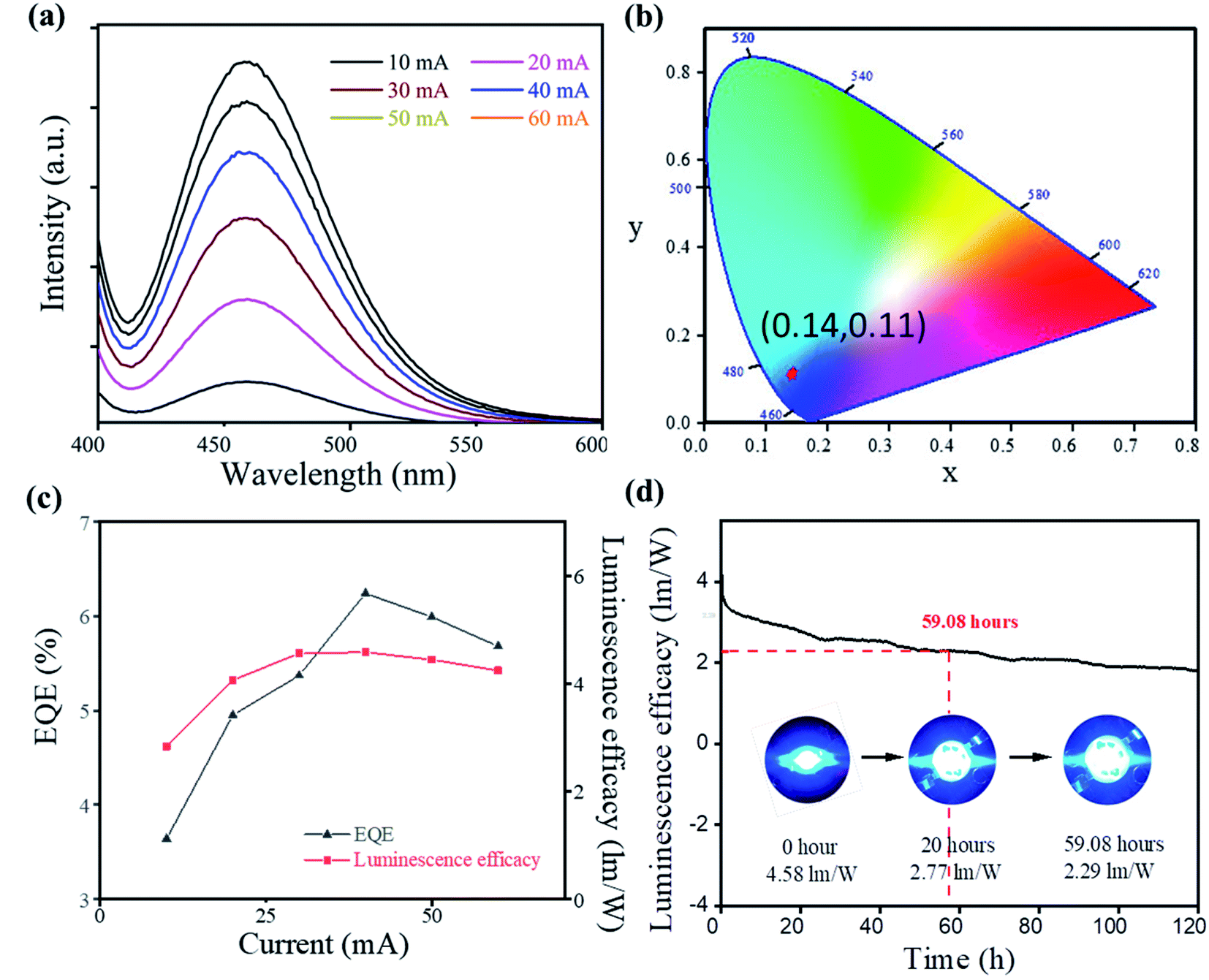 | ||
| Fig. 4 Blue LED device performance of Cs2SnCl6:Bi3+ (0.100 mol L−1): (a) the photoluminescence spectra at different currents. (b) CIE chromaticity coordinates of the blue LED. (c) EQE and luminescence efficacy at different currents. (d) Luminescence efficacy spectra of 120 h. Inset: photo images of the devices. | ||
Furthermore, a maximum EQE of 6.24% and a luminous efficiency of 4.6 lm W−1 were obtained at 40 mA. More importantly, the device demonstrated an excellent stability, and time-dependent luminescence efficacy spectra appeared after 59.08 hours of continuous current. After 120 hour work, the device still showed good blue emission. The TGA measurement also showed a good thermal stability of the sample (Fig. S4†). The high thermal stability and the pure blue emission of Cs2SnCl6:Bi3+ made it a promising potential candidate for the blue-emitting LEDs.
A Bi3+-doped Cs2SnCl6 was synthesized via a solution-phase route with varied precursor concentrations. The nucleation density and the quality of crystal nucleus growth could be tuned by the precursor concentration, which could affect the crystal morphology, the Bi3+ doping amount, and the photophysical properties of Bi3+-doped Cs2SnCl6. The nucleus growth process was accompanied by [BiSn + VCl] formation, which enhanced the luminescence intensity and extended the exciton delay time. The larger crystallite size was synthesized at 0.100 mol L−1 concentration, with a highest PL intensity (456 nm, PLQY = 31%) and a most extended lifetime (378 ns) by suppressing the non-radiative process. Additionally, the samples demonstrated excellent stabilities, and the Bi3+-doped Cs2SnCl6 blue LED showed a blue emission with CIE coordinates of (0.14, 0.11), an external quantum efficiency (EQE) of 6.24%, and a luminescence power of 4.6 lm W−1. The device continued to work for 120 hours. This work suggested that Cs2SnCl6:Bi3+ possessed great potential in future light-emitting applications.
Data statement
The data that support the findings of this study are available from the corresponding author upon reasonable request.Conflicts of interest
There are no conflicts of interest to declare.Acknowledgements
We thank the funding support from the Shenzhen Municipal Development and Reform Commission, New Energy Technology Engineering Laboratory (Grant Number: SDRC [2016]172) and the Shenzhen Science and Technology Innovation Committee (JCYJ20190809172615277).References
- H. Zhang, L. Zhu, J. Cheng, L. Chen, C. Liu and S. Yuan, Crystals, 2019, 9, 258 CrossRef CAS.
- H. Zhang, L. Zhu, J. Cheng, L. Chen, C. Liu and S. Yuan, Materials, 2019, 12, 1501 CrossRef CAS PubMed.
- Z. Wu, Q. Zhang, B. Li, Z. Shi, K. Xu, Y. Chen, Z. Ning and Q. Mi, Chem. Mater., 2019, 31, 4999 CrossRef CAS.
- Z. Tan, J. Li, C. Zhang, Z. Li, Q. Hu, Z. Xiao, T. Kamiya, H. Hosono, G. Niu, E. Lifshitz, Y. Cheng and J. Tang, Adv. Funct. Mater., 2018, 28, 1801131 CrossRef.
- A. Yan, K. Li, Y. Zhou, Y. Ye, X. Zhao and C. Liu, J. Alloys Compd., 2020, 822, 153528 CrossRef CAS.
- C. Zhang and J. Lin, Chem. Soc. Rev., 2012, 41, 7938 RSC.
- S. Wang, M. Chen, W. Zhang, Y. Han, P. Shi, Y. Guo, Z. Mu, X. L. Lu, Z. Zhang and A. Song, Inorg. Chem. Commun., 2021, 124, 108372 CrossRef CAS.
- G. Engel, Naturwissenschaften, 1933, 21, 704 CrossRef CAS.
- H. Miao, C. Ding and H. Luo, Microelectron. Eng., 2003, 66, 142 CrossRef CAS; Y. Zhou, Z. J. Yong, K. C. Zhang, B. M. Liu, Z. W. Wang, J. S. Hou, Y. Z. Fang, Y. Zhou, H. T. Sun and B. Song, J. Phys. Chem. Lett., 2016, 7, 2735 CrossRef PubMed.
- B. Xie, E. Liu, G. Bai, R. Ye and S. Xu, J. Lumin., 2021, 230, 1 CrossRef CAS; J. Zheng, Q. Cheng, S. Wu, Z. Guo, Y. Zhuang, Y. Lu, Y. Li and C. Chen, J. Mater. Chem. C, 2015, 3, 11219 RSC.
- C. Y. Wang, P. Liang, R. J. Xie, Y. Yao, P. Liu, Y. Yang, J. Hu, L. Shao, X. W. Sun, F. Y. Kang and G. D. Wei, Chem. Mater., 2020, 32, 7814 CrossRef CAS.
- R. W. Brower, S. Meij and P. W. Serruys, Cardiovasc. Res., 1983, 17(8), 482–488 CrossRef CAS PubMed.
- M. Wang, B. Li, J. Yuan, F. Huang, G. Cao and J. Tian, ACS Appl. Mater. Interfaces, 2018, 10, 37005 CrossRef CAS PubMed.
- A. A. B. Baloch, F. H. Alharbi, G. Grancini, M. I. Hossain, M. K. Nazeeruddin and N. Tabet, J. Phys. Chem. C, 2018, 122, 26805 CrossRef CAS; D. Yan, T. Shi, Z. Zang, T. Zhou, Z. Liu, Z. Zhang, J. Du, Y. Leng and X. Tang, Small, 2019, 15, 1901173 CrossRef PubMed.
- K. Li, M. Shang, H. Z. Lian and J. Lin, J. Mater. Chem. C, 2015, 3, 9990 Search PubMed; S. F. Zhou, B. Zhu, H. C. Yang, S. Ye, G. Lakshminarayana, J. H. Hao and J. R. Qiu, Adv. Funct. Mater., 2008, 18(9), 1407 CrossRef CAS.
- J. Zhou, Z. Xia, M. S. Molokeev, X. Zhang, D. Peng and Q. Liu, J. Mater. Chem. C, 2017, 5, 15031 RSC.
- A. Kaltzoglou, M. Antoniadou, A. G. Kontos, C. C. Stoumpos, D. Perganti, E. Siranidi, V. Raptis, K. Trohidou, V. Psycharis, M. G. Kanatzidis and P. Falaras, J. Phys. Chem. C, 2016, 120, 11777 CrossRef CAS.
- J. Song, J. Li, X. Li, L. Xu, Y. Dong and H. Zeng, Adv. Mater., 2015, 27, 7162 CrossRef CAS PubMed; K. Lin, J. Xing, L. N. Quan, F. P. G. de Arquer, X. Gong, J. Lu, L. Xie, W. Zhao, D. Zhang, C. Yan, W. Li, X. Liu, Y. Lu, J. Kirman, E. H. Sargent, Q. Xiong and Z. Wei, Nature, 2018, 562, 245 CrossRef PubMed; W. Deng, X. Xu, X. Zhang, Y. Zhang, X. Jin, L. Wang, S.-T. Lee and J. Jie, Adv. Funct. Mater., 2016, 26, 4797 CrossRef; E. P. Yao, Z. Yang, L. Meng, P. Sun, S. Dong, Y. Yang and Y. Yang, Adv. Mater., 2017, 29, 1606859 CrossRef PubMed.
Footnotes |
| † Electronic supplementary information (ESI) available: Experimental section, Fig. S1–S4, and Tables S1 and S2. See DOI: 10.1039/d1ra03622j |
| ‡ These authors contributed equally to this work. |
| This journal is © The Royal Society of Chemistry 2021 |