
 Open Access Article
 This Open Access Article is licensed under a Creative Commons Attribution-Non Commercial 3.0 Unported Licence
Facile fabrication and low-temperature bonding of Cu@Sn–Bi core–shell particles for conductive pastes†
Zhehan Yang,
Yi Pan,
Hengyu Zhao,
Xiangmin Yang,
Ying Liang,
Zhen Zhang * and
Bin Fang*
* and
Bin Fang*
Institute of Nuclear Technology and Application, School of Science, East China University of Science and Technology, Shanghai 200237, P. R. China. E-mail: zhangzhen@ecust.edu.cn; binfang@ecust.edu.cn
First published on 2nd August 2021
Abstract
The rapid development of flexible wearable electronics arouses huge demand for low-temperature sintering metal inks applied to temperature-sensitive substrates. The high sintering temperature and easy oxidation limited the application of Cu-based pastes. A two-step method involving liquid co-reduction and heat ripening was developed to synthesize Cu@Sn–Bi core–shell particles. The thickness of Sn–Bi shells can be flexibly adjusted via changing the mass ratio of Cu to Sn–Bi. The volume resistivity of printed circuits using Cu@Sn–Bi pastes solidified at 200 °C was as low as 481 μΩ cm, which increased by 11.8% after an aging process at 190 °C for 6 h. The outstanding stability in a harsh environment would attribute to the effective protection of Sn–Bi alloy shells. This work suggests a new pathway toward the low-temperature bonding and anti-oxidation of Cu particles as conductive fillers, which can be widely applied to the additive manufacturing of flexible wearable electronics.
Introduction
Additive manufacturing technology has attracted increasing attention towards printed circuit boards (PCBs) and integrated circuits (ICs) because it provides enormous potential and opportunities for the production of diverse electronic devices such as multi-axial sensors, wearable electronic equipments and e-skins for robotics applications.1–3 The conventional subtractive manufacturing has many drawbacks including complex process, long production cycle, and serious environmental pollution.4,5 Inkjet printing or screen printing served as low cost, simple implementation and environmentally friendly technologies that can be utilized directly for conductive patterns.6 As one of the key materials of printed electronic technology, conductive inks needed much effort, which were mainly divided into conductive adhesives7,8 consisting of polymers and conductive fillers, and conductive pastes9–11 consisting of dispersion and conductive fillers. In both kinds of conductive inks, the properties of conductive fillers are of great importance. Conductive fillers mainly include carbon-based materials (such as graphenes, graphene oxides and carbon nanotubes),12,13 transparent conductive oxides (such as In2O3, ZnO and SnO2)14,15 and metallic nano-micro fillers (such as Cu or Ag nanoparticles).16,17Metal fillers have distinct advantages in mechanical property, ductility and electrical conductivity. However, the contradiction between the high sintering temperature of metals and the low temperature resistance of flexible polymeric substrates limits the use of metal fillers. In particular, the rapid development of flexible wearable electronics arouses huge demand for low-temperature sintering metal inks. Compared with their bulk counterparts, the melting point of the nanoscale metallic particles can be dramatically lowered by decreasing their size based on the size effect of nanomaterials, making them suitable for heat-sensitive substrates.18 Lee et al. reported that conductive ink consists of Cu nanoparticles (NPs) with a diameter of 30–65 nm.19 The lowest resistivity was 3.6 × 10⁻⁶ Ω cm after 60 min of sintering at 200 °C under N2 flow. Yabuki et al. synthesized conductive pastes via dispersing Cu NPs (about 20 nm) into α-terpineol (50 wt%), and a 3 × 10⁻⁵ Ω cm resistivity of copper patterns was achieved after 60 min of sintering at 300 °C under 5% H2–Ar.20
In these studies, the diameter of Cu NPs has been very severe, and could be easily oxidized upon contact with air. Even worse, the oxidation process occurs not only during the synthesis, but also in every step of applications such as storage, printing and sintering. Sn–Bi is a kind of low-melting point alloys, of which the lowest melting temperature is 137 °C. Faiz et al. reported fluxless bonding of plateless Cu–Cu substrates at a processing temperature lower than 250 °C, and a low pressure of 0.1 MPa was achieved by transient liquid-phase sintering of mixed Cu NPs and Sn–Bi eutectic powders.21 This proves the possibility of employing Cu and Sn–Bi mixtures in low-temperature conductive pastes. However, the mixture composition of Cu NPs and Sn–Bi alloy particles could not avoid the oxidation of Cu efficiently. The core–shell structure of Cu@Sn–Bi would be able to protect Cu cores against oxidation and maintain the high conductivity of the original fillers.
Herein, a two-step method to synthesize Cu@Sn–Bi core–shell microparticles that served as conductive fillers was proposed. The as-synthesized fillers were made into conductive pastes, which were printed and could be fused by Sn–Bi shells below 200 °C. Different thicknesses of the alloy shells can be obtained by changing the mass ratio of Cu seeds to Sn–Bi precursors. The volume resistivity of the printed circuit made from Cu@Sn–Bi particles and water-based fluxes was as low as 481 μΩ cm. After an aging process at 190 °C for 6 h, the volume resistivity increased by about 11.8%. The outstanding stability in a harsh environment would attribute to the effective protection of the alloy shell. The expected significance of this work is the development of a new pathway toward the low-temperature bonding and anti-oxidation of Cu particles as conductive fillers, which can be widely applied to the additive manufacturing of flexible wearable electronics.
Experimental
Materials
Stannous chloride (SnCl2, AR), bismuth nitrate pentahydrate (Bi(NO3)3·5H2O, AR), sodium hydroxide (NaOH, AR), poly(vinyl pyrrolidone) (PVP, K30), diethylene glycol (DEG, 99%), ethanol (98%), glycol (98%), acetic acid (99.5%) and sodium borohydride (NaBH4, 98%) were purchased from Shanghai Titan Scientific Co., Ltd. Rosin-free flux and Cu particles (d0 ≈ 1.60 μm) were purchased from Shanghai Likai Material Technology Co., Ltd. All chemicals were used as received without further purification.Synthesis of Cu@Sn–Bi core–shell particles
Cu@Sn–Bi core–shell particles were synthesized by a two-step process. In the first step, Sn and Bi NPs with several nanometers of diameter were synthesized by a liquid co-reduction method. For this purpose, 3.40 g SnCl2, 6.70 g Bi(NO3)3·5H2O and 0.89 g PVP were added into 60.00 mL DEG and named solution A. Then, 0.39 g PVP and 3.28 g NaBH4 were dissolved into 60.00 mL DEG and named solution B, which was put into an ice-salt bath and held at −5 °C. Solution B was stirred and bubbled by N2 to remove O2, and then solution A and 67.00 mL saturated ethanol solution of NaOH were dropped into solution B using a peristaltic pump at a rate of 1.80 mL min−1 synchronously. After dropping, the dispersion was returned and stored at room temperature for the next step.In the second step, the Cu particles were covered with a Sn–Bi alloy via a heat ripening process. In a typical experiment, 4.00 g Cu particles were treated with 5% acetic acid solution (50.00 mL) for 10 min to remove the oxide layer. Next, Cu particles were washed three times with deionized water and ethanol, respectively, and dispersed into 4.00 mL ethanol to obtain the dispersion (1.00 g mL−1). The Cu particle dispersion was added into the Sn and Bi NPs dispersion synthesized in the first step. The system was heated to 130 °C to steam out the ethanol (about 71.00 mL). Then, the system was heated at 160 °C for 30 min and 180 °C for 10 min, respectively. Finally, the oil bath was removed and the system was cooled down in air rapidly. The protection of N2 was employed in the whole heat ripening process. The products were washed by centrifugation (8000 rpm, 10 min) and re-dispersion cycled with ethanol and deionized water to remove the remaining reactants, and dried at 60 °C for 3 h in a vacuum oven.
In order to adjust the thickness of the Sn–Bi shell, the Cu particle dispersion with different volumes (1.00 mL, 2.00 mL, 4.00 mL, 6.00 mL) was adopted, which were marked Cu@Sn–Bi-0.2, Cu@Sn–Bi-0.4, Cu@Sn–Bi-0.8, and Cu@Sn–Bi-1.2 respectively. In addition, different stirring speeds (90 rpm, 180 rpm, 240 rpm and 300 rpm) were adopted to examine its influence on morphology. The experimental conditions are summarized in Table S1 (ESI†).
Preparations of solder paste and printed circuit
The solder paste was prepared by mixing Cu@Sn–Bi particles with rosin-free flux and glycol. Then, 3.00 g glycol and 3.00 g flux were mixed with 15.00 g Cu@Sn–Bi particles preliminarily. The paste was further processed by a three rollers mixer. The width of feeding and discharge gaps was 30 and 15 μm, respectively. The speed of discharge roller was 240 rpm.The circuits were printed by screen printing using Cu@Sn–Bi pastes. The aperture and thickness of screen are 40 and 12 μm, respectively. The circuits were dried at 90 °C for 10 min in a N2 atmosphere to facilitate the evaporation of organic solutions and melt of flux, which were beneficial for improving its wettability on the surface of particles. Then, the printed circuit was heated and solidified at different temperatures. To investigate the effects of the solidifying temperature and the ratio of Cu to Sn–Bi alloy on the conductivity and microstructure, different solidifying temperatures (160–240 °C) were selected.
Characterization
Scanning electron microscopic (SEM) images were acquired using a Nava Nano SEM450 scanning electron microscope (FEI, USA) at 3.0 kV accelerating voltage. Powder X-ray diffraction (PXRD) patterns were recorded using a rotating anode X-ray powder diffractometer (D/max2550VB/PC18KW, Japan) equipped with graphite monochromatized Cu Kα radiation (λ = 1.54178 Å). The elemental composition and internal structure were determined by energy-dispersive spectroscopy (EDS) using a field emission scanning electron microscope (Gemini SEM 500, Japan) operating at 3.0 kV equipped with an extreme windowless 100 mm detector with electric refrigeration. Differential scanning calorimetry (DSC) was conducted at a heating rate of 10 °C min−1 in a N2 atmosphere (DSC 8500, China).Thickness measurement of Sn–Bi shells of Cu@Sn–Bi particles
The Cu@Sn–Bi particles were dissolved in nitric acid (65–68 wt%) and diluted with deionized water. The mass contents of Cu2+, Sn2+, and Bi3+ in the solution were determined by inductively coupled plasma atomic emission spectroscopy (ICP-AES) using an Agilent 725 ICP-OES (USA).The average diameter of Cu particles is 1.60 μm. The densities of Sn, Bi and Cu are 7.28 g cm−3, 9.78 g cm−3 and 8.96 g cm−3, respectively. The thickness of the Sn–Bi alloy shell was calculated using formula (1):
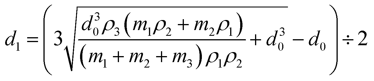 | (1) |
Test of volume resistivity
The tested volume resistivity (ρtest) of the conductive circuit was directly measured using a portable four-probe resistance tester (Jingge M-6, Suzhou Jingge Electronic Co., Ltd, China) equipped with four tungsten probes. The thickness was measured using a spiral micrometer. Then, the volume resistivity (ρ) was calculated using formula (2):
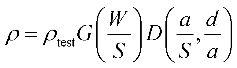 | (2) |
Test of flexibility
In order to characterize the flexibility of printed circuits, which were printed on the polyimide (PI) film and solidified at 200 °C, the flexible property was studied under mechanical stress by measuring the electrical resistivity after bending the PI sheet around the cylinder with a radius of 10 mm.Results and discussion
The Sn and Bi precursors were synthesized by a liquid co-reduction method. The mixed solution of Sn and Bi salts was dropped into a reductant solution. Meanwhile, in order to inhibit the decomposition of NaBH4, the NaOH solution was added at the same speed to adjust the pH between 8 and 12. Upon addition of the salt solution droplet into the reductant solution, Sn2+ and Bi3+ were reduced immediately. The small-sized Sn and Bi crystal nuclei co-precipitated from the solution. Along with the addition of the salt solution, the growth of Sn and Bi nuclei was carried on. The mixtures of Sn and Bi NPs with a diameter ranging from 3 to 10 nm were obtained, as shown in Fig. 1a. Due to the closed oxidation reduction potential, Sn2+ (−0.91 V) and Bi3+ (−0.60 V) were co-reduced at the same time. In particular, co-reduction would be helpful to the uniform distribution of Sn and Bi clusters, which agglomerated into the Sn and Bi NPs mixtures. The well-mixed Sn and Bi were beneficial for the formation of Sn–Bi alloys. In the meantime, the reaction was performed at −5 °C, and the low temperature was not only helpful for shrinking the size but also good for limiting the crystallinity of the Sn and Bi NPs mixtures. As shown in Fig. 1b, specifically, the diffraction peaks of Sn and Bi NPs mixtures were weak. The crystallinity was close to the amorphous state, which would significantly reduce the melting temperature. Fig. S1 (ESI†) shows the DSC result of Sn and Bi NPs mixtures, and there was no obvious endothermic peak, which means the mixtures had no definite melting point. Hence, the Sn, Bi or Sn–Bi alloys with high crystallinity did not form, which is in accordance with the PXRD result.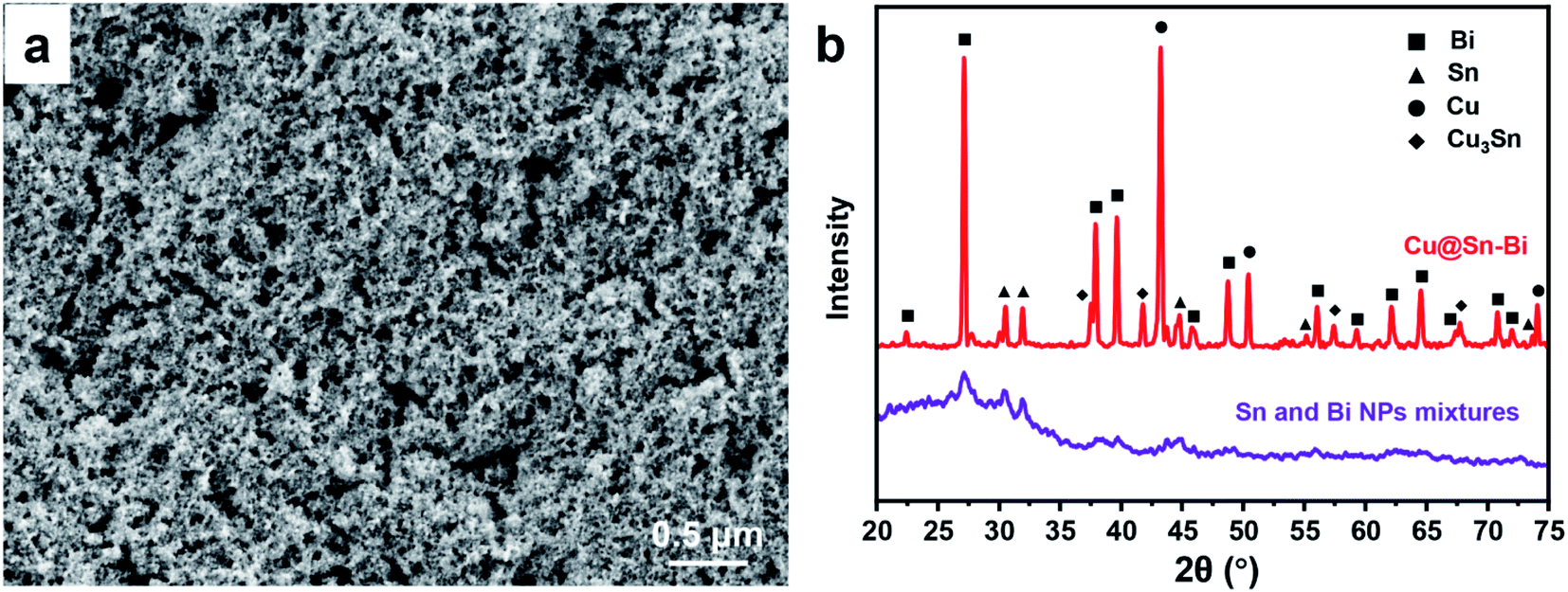 | ||
| Fig. 1 (a) SEM image of the Sn and Bi NP mixtures taken at 3.0 kV accelerating voltage. (b) PXRD patterns of Sn and Bi NP mixtures and Cu@Sn–Bi-0.8 (300 rpm). | ||
In the heat ripening process, the Cu particles were added and served as seed spheres, as shown in the scheme (Fig. 2). Along with the rise in temperature, the ethanol evaporated totally. Furthermore, the system was heated at 160 °C for 30 min and 180 °C for 10 min, respectively. The Sn and Bi NPs mixtures melt and ripen to obtain Sn–Bi alloys. In order to form the core–shell structure, mechanical stirring was adopted. The Sn–Bi alloys and Cu seeds were mixed uniformly under stirring, and the collision and coalescence between Sn–Bi alloys and Cu seeds happened. When the temperature cooled down immediately under stirring, the core–shell Cu@Sn–Bi structure was obtained. In Fig. 3a, the surface of Cu particles was relatively smooth. After the coating of Sn–Bi alloys, the morphology of Cu seeds changed obviously. The Sn–Bi alloy nucleated and grew on the surface of Cu cores, and thus, the surface became rough, and the diameter increased from 1.60 to 1.81 μm (Fig. 3b).
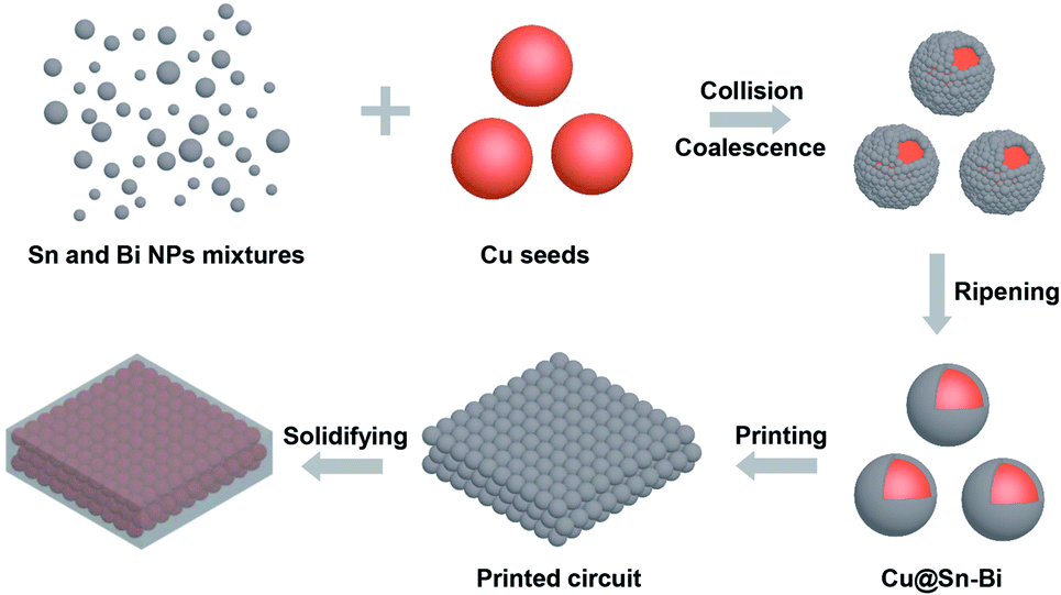 | ||
| Fig. 2 Schematic of the synthesis of Cu@Sn–Bi and solidification of printed circuits using Cu@Sn–Bi pastes. | ||
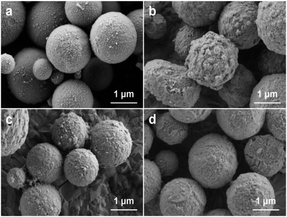 | ||
| Fig. 3 SEM images of Cu particles (a) and Cu@Sn–Bi core–shell particles synthesized under different stirring rates: 180 rpm (b), 240 rpm (c) and 300 rpm (d). All SEM images were taken at 3.0 kV accelerating voltage. | ||
The stirring was crucial for the formation of core–shell Cu@Sn–Bi structures. Only the speed of stirring was fast enough to the uniform dispersion of the Sn–Bi alloy and Cu seeds, and the core–shell structure would be obtained. When the speed was lower than 180 rpm, the multiple Cu seeds were covered together by the Sn–Bi alloy to form the multicore structure or millimeter-scale bulk (Fig. S2, ESI†). The surface of the Sn–Bi alloy coating became smooth with the increase in stirring rate (from 180 rpm to 300 rpm), as shown in Fig. 3. To consider both the stable stirring rate and smoothness, 300 rpm was chosen. When the commercially available Sn–Bi alloy particles (10 ≤ d ≤ 25 μm) were used as the precursor, they directly melted and agglomerated into a large bulk of alloy and Cu particles, sinking to the bottom of the flask (Fig. S3, ESI†). This phenomenon could further prove that the Sn and Bi NPs mixtures with a small size and low crystallinity were crucial to the formation of the core–shell structure.
In order to further confirm the structure and component of Cu@Sn–Bi, detailed characterizations were performed. Fig. 4 shows the SEM and EDS mapping images for Cu@Sn–Bi samples (Cu@Sn–Bi-0.8, 300 rpm). Clearly, the Cu, Sn and Bi elements were homogeneously distributed across the composite microsphere. The size of Cu element distributed region was about 1.60 μm, which was slightly narrower than the distributed zones of Sn and Bi elements. This could prove that the Sn–Bi alloy was shell coated on the Cu seed, and the core–shell structure was obtained.
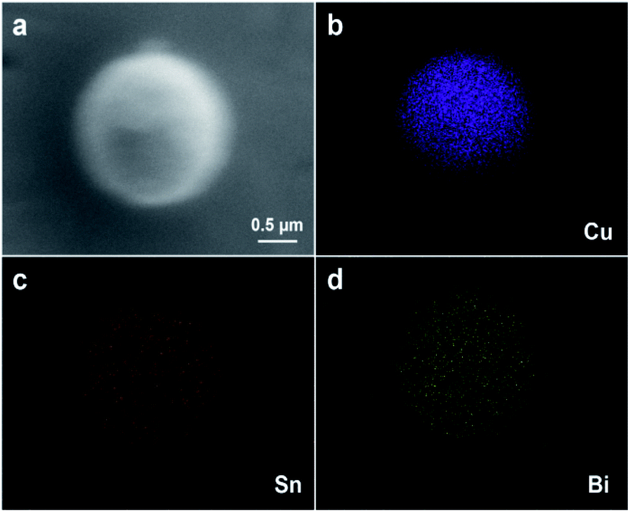 | ||
| Fig. 4 (a) SEM image of the Cu@Sn–Bi sample (Cu@Sn–Bi-0.8, 300 rpm), and the corresponding EDS mapping images of Cu (b), Sn (c), and Bi (d). All images were taken at 3.0 kV accelerating voltage. | ||
Fig. 1b shows the PXRD pattern of Cu@Sn–Bi: the characteristic peaks located at 2θ = 22.40°, 27.18°, 37.92°, 39.66°, 46.02°, 48.70°, 56.02°, 59.34°, 62.18°, 64.56°, 67.40°, 70.80° and 71.88° could be assigned to the (003), (012), (104), (110), (113), (202), (024), (107), (116), (122), (018), (214) and (300) planes of the hexagonal Bi structure (JCPDS: 44-1246), respectively.22 The diffraction peaks at 2θ = 30.60°, 32.04°, 44.80°, 55.20° and 73.68° coincide with the (200), (101), (211), (301) and (411) planes of the tetragonal Sn structure (JCPDS: 04-0673), respectively.23 In addition, the diffraction peaks at 2θ = 43.28°, 50.42° and 74.08°, coincide with the (111), (200) and (220) planes of the cubic Cu structure (JCPDS: 04-0836).24 The diffraction peaks at 2θ = 37.54°, 41.82°, 57.40° and 67.86°, coincide with the (0 16 0), (002), (0 16 2) and (083) planes of the orthorhombic Cu3Sn structure (JCPDS: 01-1240), respectively.25 Thus, these diffraction peaks are identified as Bi, Sn, Cu and Cu3Sn phases mainly formed during the ripening process. Compared with Sn and Bi NPs mixtures, the crystallinity of the alloy products is obviously enhanced.
Fig. 5 shows the DSC curve of Cu@Sn–Bi-0.8 (300 rpm), and two endothermic peaks appeared at 139.1 and 269.3 °C, which correspond to the melting points of the Sn–Bi eutectic alloy and pure Bi, respectively. The pure Bi might crystallize into nanoparticles and mix with Cu@Sn–Bi composite particles. This is because the liquid component cooled back to eutectic point along with the precipitation of Bi during the cooling process.26 There was no melting event of Sn at approximately 231.9 °C. The Sn of the product formed either the Sn–Bi alloy or Cu3Sn. In the process of heat treatment, some Sn combined with Cu to form Cu3Sn, distributed on the surface of Cu cores.
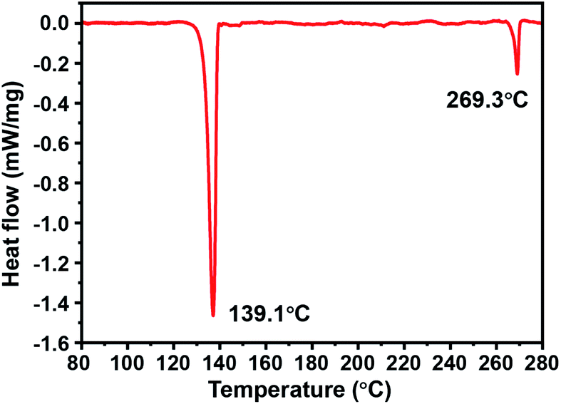 | ||
| Fig. 5 DSC curve of Cu@Sn–Bi-0.8 (300 rpm). | ||
The thickness of Sn–Bi shells can be flexibly adjusted by changing the mass ratio of Cu to Sn–Bi. In addition, the mass ratio of Cu to Sn–Bi ranging from 0.2 to 1.2 was adopted, the corresponding products were marked as Cu@Sn–Bi-0.2, Cu@Sn–Bi-0.4, Cu@Sn–Bi-0.8, and Cu@Sn–Bi-1.2, respectively. Furthermore, the contents of Cu2+, Sn2+, and Bi3+ were determined by ICP-AES to investigate the variation of thickness calculated using formula (1). Along with the growth of mass ratio of Cu to Sn–Bi, the contents of Cu increased from 26 to 71%, and the thickness of Sn–Bi shells decreased from 166 to 78 nm (Table 1). This phenomenon is in line with the experimental expectation. Meanwhile, we can find that the content of Sn was higher than that of Bi due to the formation of Cu3Sn. This was also verified by PXRD and DSC results.
| Sample | The mass ratio of Cu to Sn–Bi | Elemental content | Thickness of Sn–Bi alloy shell (nm) | ||
|---|---|---|---|---|---|
| Cu (%) | Sn (%) | Bi (%) | |||
| Cu@Sn–Bi-0.2 | 1![[thin space (1/6-em)]](https://www.rsc.org/images/entities/char_2009.gif) :5 :5 |
26 | 46 | 28 | 166 |
| Cu@Sn–Bi-0.4 | 2:5 |
44 | 36 | 20 | 132 |
| Cu@Sn–Bi-0.8 | 4:5 |
59 | 23 | 18 | 113 |
| Cu@Sn–Bi-1.2 | 6:5 |
71 | 18 | 11 | 78 |
Next, the Cu@Sn–Bi particles served as conductive fillers mixed with flux and glycol to fabricate the solder pastes. In addition, the three rollers mixer was used for blending thoroughly. The circuit was printed through screen printing using the Cu@Sn–Bi paste, which was dried and solidified at different temperatures (160–240 °C) in a N2 atmosphere. Along with the evaporation of organic solutions and the melt of flux, the Sn–Bi shells melted and fused together. The Cu cores were bonded at low temperatures (Fig. 2). The appearance of circuits solidified at 200 °C is shown in the inset of Fig. 6, the colour of the circuit is silvery white, which is the result of melting and reflow of Sn–Bi alloy shells. Thus, the conductive path was obtained through bonding the Cu particles using the Sn–Bi alloy at low temperatures.
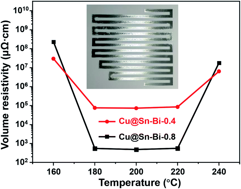 | ||
| Fig. 6 Volume resistivity of printed circuits using Cu@Sn–Bi pastes solidified at different temperatures and the digital photograph of the circuit (inset) using Cu@Sn–Bi-0.8 paste solidified at 200 °C. | ||
The volume resistivity (ρ) of the conductive path was measured by a four-probe method and calibrated using formula (2). As shown in Fig. 6 and Table S2 (ESI†), when the solidified temperature was at 160 °C, though it exceeds the melting point of the Sn–Bi alloy, the acceptable conductivity of the Cu@Sn–Bi-0.2 paste was undetected. When the solidified temperature increased from 160 to 200 °C, ρ decreased rapidly, and the lowest ρ value (481 μΩ cm) of the Cu@Sn–Bi-0.8 sample was obtained. With the solidified temperature continuing to increase and exceed 220 °C, the ρ value grew rapidly and reached 1.80 × 10⁷ μΩ cm at 240 °C. The molten Sn infiltrated into the Cu core and formed a thick intermetallic compound layer, which greatly improves the volume resistivity. The mass ratio of Cu to Sn–Bi also played a major influence on the conductivity of printed circuits. Along with the decrease in Cu content, the ρ increased dramatically, and the ρ of Cu@Sn–Bi-0.4 and Cu@Sn–Bi-0.2 pastes reached 7.34 × 10⁴ and 6.52 × 10⁶ μΩ cm after solidification at 200 °C. This may be because the content of Cu serving as a good conductor decreased. When the mass ratio of Cu to Sn–Bi increased from 0.8 to 1.2, the electrical conductivity also decreased significantly. In addition, the circuits using Cu@Sn–Bi-1.2 as a conductive filler were insulative, that is because the Sn–Bi alloy shells are too thin to bond the Cu cores together. Thus, the solidification temperature and the thickness of the Sn–Bi alloy shell show significant influences on the electrical conductivity of printed circuits.
Furthermore, the microstructures of printed circuits (Cu@Sn–Bi-0.8) solidified at different temperatures (160–200 °C) were examined carefully using SEM to clarify the difference of the electrical conductivity. When the heating temperature exceeds 139 °C, the Sn–Bi alloy shell would melt and bond Cu particles together, but the bonding between particles was poor when solidified at 160 °C. There were obvious grain boundaries observed (Fig. 7a). It is because that the soldering temperature is too low, the flux can not volatilize in time. The fluidity of Sn–Bi alloy is poor at a relatively low temperature.27 Thus, the ρ value of the corresponding circuit was as high as 2.34 × 10⁸ μΩ cm. Along with the increase in soldering temperatures to 180 and 200 °C, the Cu particles were connected together by Sn–Bi alloy shells and the grain boundary disappeared gradually (Fig. 7b and c). In addition, the Cu, Sn and Bi elements were homogeneously distributed across the conductive path (Fig. 7d).
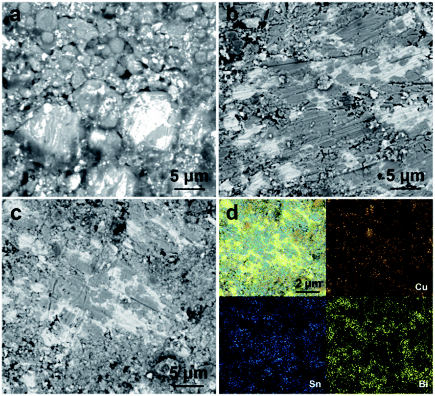 | ||
| Fig. 7 SEM images of printed circuits using the Cu@Sn–Bi-0.8 paste solidified at different temperatures: 160 °C (a), 180 °C (b) and 200 °C (c). (d) The corresponding EDS mapping images of (c) for Cu, Sn and Bi elements. All images were taken at 3.0 kV accelerating voltage. | ||
In addition, the cross-sectional morphology of the printed circuit (Cu@Sn–Bi-0.8) solidified at 200 °C was examined (Fig. S4, ESI†). The Cu spheres marked with dotted lines were soldered and bonded together by the melt and solidification of Sn–Bi alloy shells. Thus, the conductive path consisting of both Cu and Sn–Bi alloys alternately was obtained and the ρ decreased remarkably. Although the lowest ρ (481 μΩ cm) is further larger than the metallic Cu, which is close to the reported Cu-based inks ranging from dozens to a thousand μΩ cm, as shown in Table S3 (ESI†). The relative low electrical conductivity would be attributed to that the Cu particles were bonded together using Sn–Bi alloys rather than the sintering of Cu particles themselves. In addition, the voids can be observed (Fig. S4, ESI†), which may be another reason for the high volume resistivity.
Generally, the size of Cu NPs is controlled in nanometer scale to decrease the sintering temperature, which was easily oxidized. In this work, the diameter of Cu@Sn–Bi fillers is at the micron level. The larger size and Sn–Bi alloy protection were beneficial for antioxidants during the synthesis, solidification and long-term working procedures. After an aging process at 190 °C for 6 h, the volume resistivity increased by about 11.8% (Fig. S5, ESI†). Therefore, the Cu@Sn–Bi-based paste could protect Cu against oxidation and maintain the high conductivity in a harsh environment.
The low curing temperature of the Cu@Sn–Bi-0.8 paste could meet the demand of the flexible polymer substrate. The soft circuits printed on the PI film were solidified at 200 °C, as shown in Fig. S6a (ESI†). In addition, the flexible property was studied under mechanical stress by measuring the electrical resistivity after bending the PI sheet around the cylinder with a radius of 10 mm. After 100 cycles of repetitive strain around the cylinder, the ρ value of the conductive path increased from 481 to 503 μΩ cm (about 4.6% growth). In the meantime, no fracture or shelling of circuits was observed (Fig. S6b ESI†). The excellent flexibility of circuits could be attributed to the low-temperature soldering of the Cu@Sn–Bi paste. The Cu cores and Sn–Bi shells were bonded together to form monoblock circuits showing the metallic ductility.
Conclusion
It was proved that a two-step method involving liquid co-reduction and heat ripening was developed to synthesize Cu@Sn–Bi core–shell particles, which could serve as fillers for conductive pastes to fuse the Cu particles at low temperatures. The thickness of the Sn–Bi alloy shell and the solidifying temperature show significant influences on the electrical conductivity of printed circuits. In addition, the lowest ρ (481 μΩ cm) was obtained, about 11.8% growth happened after 6 h aging at 190 °C. The outstanding stability would attribute to the effective protection of the Sn–Bi alloy shell. This work provides new insights into the low-temperature bonding and anti-oxidation protection of Cu particles for additive manufacturing of flexible wearable electronics.Conflicts of interest
There are no conflicts to declare.Acknowledgements
The authors thank Research Center of Analysis and Test, 985 test platform of School of Chemical Engineering of East China University of Science and Technology for the technique support.Notes and references
- D. M. Vogt, Y.-L. Park and R. J. Wood, IEEE Sens. J., 2013, 13(10), 2056–4064 Search PubMed.
- Z. Shao, X. Hu, W. Cheng, Y. Zhao, J. Hou, M. Wu, D. Xue and Y. Wang, Nanoscale, 2020, 12, 18771–18781 RSC.
- R. P. Rocha, P. A. Lopes, A. T. de Almeida, M. Tavakoli and C. Majidi, J. Micromech. Microeng., 2018, 28, 034001 CrossRef.
- O. Y. Makovskaya, A. P. Shevchuk and S. P. Sorokin, Solid State Phenom., 2020, 299, 998–1004 Search PubMed.
- K. J. Lee, B. H. Jun, T. H. Kim and J. Joung, Nanotechnology, 2006, 17, 2424–2428 CrossRef CAS.
- J. Zhang, Z. B. Liang, T. Hreid, W. Guo and Z. B. Yuan, RSC Adv., 2012, 2, 4787–4791 RSC.
- Q. Yan, M. Zhou and H. Fu, J. Mater. Chem. C, 2020, 8, 7772–7785 RSC.
- H.-W. Cui, J.-T. Jiu, S. Nagao, T. Sugahara, K. Suganuma, H. Uchida and K. A. Schroder, RSC Adv., 2014, 4, 15914–15922 RSC.
- M. Wang, X. F. Xu, B. Ma, Y. Y. Pei, C. C. Ai and L. J. Yuan, RSC Adv., 2014, 4, 47781–47787 RSC.
- J. Lee, J. Jun, W. Na, J. Oh, Y. Kim, W. Kima and J. Jang, J. Mater. Chem. C, 2017, 5, 12507–12512 RSC.
- K.-Y. Shin, J. S. Lee, J.-Y. Honga and J. Jang, Chem. Commun., 2014, 50, 3093–3096 RSC.
- D. J. Lipomi, M. Vosgueritchian, C. K. Tee, S. L. Hellstrom, J. A. Lee, C. H. Fox and Z. Bao, Nat. Nanotechnol., 2011, 6(12), 788–792 CrossRef CAS PubMed.
- M. Amjadi, Y. J. Yoon and I. Park, Nanotechnology, 2015, 26, 375501 CrossRef PubMed.
- M. Grundmann, A. Rahm and H. Wenckstern, Phys. Status Solidi A, 2015, 212(7), 1408 CrossRef CAS.
- H. Park, H. Choi, N. Lee, C. Jung, Y. Choi, S. Park, B. Kim, H. Yuk, Y. Choi, K. Kim and H. Jeon, Jpn. J. Appl. Phys., 2020, 59, 105502 CrossRef CAS.
- Y. Wu, L.-D. Liao, H.-C. Pan, L. He, C.-T. Lind and M. C. Tan, RSC Adv., 2017, 7, 29702–29712 RSC.
- H. J. Park, Y. Jo, M. K. Cho, J. Y. Woo, D. Kim, S. Y. Lee, Y. Choi and S. Jeong, Nanoscale, 2018, 10, 5047–5053 RSC.
- J. Bai, Z. Zhang and G. Lu, IEEE Trans. Compon. Packag. Technol., 2006, 29, 589–593 CAS.
- Y. Lee, J. Choi, K. J. Lee, N. E. Stott and D. Kim, Nanotechnology, 2008, 19, 415604 CrossRef PubMed.
- A. Yabuki and N. Arriffifin, Thin Solid Films, 2010, 518(23), 7033–7037 CrossRef CAS.
- M. K. Faiz, K. Bansho, T. Suga, T. Miyashita and M. Yoshida, J. Mater. Sci.: Mater. Electron., 2017, 28(21), 16433–16443 CrossRef.
- Z. Song, H. Dai and J. Tong, RSC Adv., 2015, 5, 20234–20237 RSC.
- X. Wu, C. Qian, H. Wu, L. Xu, L. Bu, Y. Piao, G. Diao and M. Chen, Chem. Commun., 2020, 56, 7629–7632 RSC.
- T. Wang, D. Wu, Y. Wang, T. Huang, G. Histand, T. Wang and H. Zeng, Nanoscale, 2018, 10, 22055–22064 RSC.
- J. Wang, J. Zou, X. Hu, S. Ning, X. Wang, X. Kang and S. Chen, J. Mater. Chem. A, 2019, 7, 27514–27521 RSC.
- V. G. Shepelevich and O. V. Gusakova, Phys. Met. Metallogr., 2009, 108, 292–297 CrossRef.
- X.-M. Zhai, Y.-F. Li, J. Zou, M.-M. Shi, B.-B. Yang, Y. Li, C.-F. Guo and R.-R. Hu, J. Electron. Mater., 2021, 50, 869–880 CrossRef CAS.
Footnote |
| † Electronic supplementary information (ESI) available. See DOI: 10.1039/d1ra02514g |
| This journal is © The Royal Society of Chemistry 2021 |