
 Open Access Article
 This Open Access Article is licensed under a
 Creative Commons Attribution 3.0 Unported Licence
Configurable switching behavior in polymer-based resistive memories by adopting unique electrode/electrolyte arrangement†
Karthik Krishnan *a,
Shaikh Mohammad Tauquira,
Saranyan Vijayaraghavana and
Ramesh Mohanb
*a,
Shaikh Mohammad Tauquira,
Saranyan Vijayaraghavana and
Ramesh Mohanb
aCorrosion and Material Protection Division, CSIR-Central Electrochemical Research Institute (CECRI), Karaikudi, TN 630-003, India. E-mail: karthikk@cecri.res.in
bMicrosystem Packaging Group, CSIR-Central Electronics Engineering Research Institute, Pilani, Rajasthan-333031, India
First published on 2nd July 2021
Abstract
The difference in resistive switching characteristics by modifying the device configuration provides a unique operating principle, which is essential for both fundamental studies and the development of future memory devices. Here, we demonstrate the poly(methyl methacrylate) (PMMA)-based resistive switching characteristics using four different combinations of electrode/electrolyte arrangement in the device geometry. From the current–voltage (I–V) measurements, all the PMMA-based devices revealed nonvolatile memory behavior with a higher ON/OFF resistance ratio (∼105–107). Significantly, the current conduction in the filament and resistive switching behavior depend majorly on the presence of Al electrode and electrochemically active silver (Ag) element in the PMMA matrix. A trap-controlled space charge limited conduction (SCLC) mechanism constitutes the resistive switching in the Al/PMMA/Al device, whereas the current conduction governed by ohmic behavior influences the resistive switching in the Ag-including devices. The depth-profiling X-ray photoelectron spectroscopy (XPS) study evidences the conducting filament formation processes in the PMMA-based devices. These results with different conduction mechanisms provide further insights into the understanding of the resistive switching behavior in the polymer-based devices by simply rearranging the device configuration.
Introduction
Easy tunable resistive switching characteristics in a metal–insulator–metal (MIM) structured device are key for the development of not only nonvolatile memories but also for future atomic electronics.1–5 In a MIM structured device, both organic (such as PEO, PVA, P3HT, etc.) and inorganic (such as Ta2O5, SiO2, ZnO, HfO2, etc.) materials serve as an ion conducting insulating dielectrics for resistive switching operation.6–13 However, the resistive switching operation mainly depends on the configuration of the electrode and electrolyte.14–17 It has been widely reported that the resistive switching in inorganic-based MIM devices arose by the valence change mechanism (VCM), in which the reduced oxygen atoms create oxygen vacancy sites in the dielectric interface for electron hopping between the electrodes during forward biasing, resulting in an ON state. Application of reverse biasing dissolves the conducting bridge between the electrodes due to the recombination of oxygen ions and oxygen vacancies, enabling an OFF state.18–21 Conversely, the organic polymer-based MIM devices operate mostly by the electrochemical metallization mechanism (ECM).22,23 In ECM cells, the subsequent growth and annihilation of conducting metallic bridge by the electrochemically active elements (such as Ag or Cu) in the dielectric polymer interface can be responsible for the ON and OFF state during respective biasing conditions.24–26 Incorporating electrochemically active elements either in electrode or electrolyte can mostly induce the filament growth and bistable resistive switching behavior. Though, the filament growth occurs randomly as stochastic events that determines the resistive switching characteristics such as forming voltage, SET and RESET voltages, ON and OFF resistance values.27,28 Significantly, the atomic constriction of thin filament results quantum transportation, where the lateral dimension of the conduction pathways are analogous to the Fermi wavelength.29,30 The highly optimized device configuration and experimental measuring conditions are prime factors influencing the atomic point contact in the conducting filament, in which the discrete quantized states (G0 = 2e2/h, where e is the charge of electron and h is Planck's constant) can be realized in MIM devices.31–34 Therefore, selecting an appropriate electrode and electrolyte material in the MIM device configuration plays crucial role in determining the filament formation and resistive switching property.Here, the PMMA-based MIM devices have been investigated for resistive switching operation using various device configurations. Four different combinations of electrode/electrolyte arrangement in the MIM structure (Al/PMMA/Al, Al/Ag/PMMA/Al, Al/AgNP-PMMA/Al and Al/Ag/AgNP-PMMA/Al) were used to demonstrate the current conduction mechanism in the filament and resistive switching characteristics. A step by step MIM device fabrication is schematically shown in Fig. 1. Owing to its good structural ordering, better thermal stability, higher ionic conductivity and easy film forming ability, PMMA can be served as an essential solid polymer electrolyte for nonvolatile memories and other applications.35–38 In general, the resistive switching behavior is significantly affected by the inherent properties of the polymer matrix such as its crystalline order, ionic conductivity and thermal stability.4,6,8 In the PMMA-based devices, the nonvolatile memory characteristics is found with large ON/OFF resistance ratio (105–107). Furthermore, the combinations of electrode/electrolyte arrangement in the MIM device structure greatly alters the resistive switching characteristics, interpreted by different conduction mechanism in the filament.
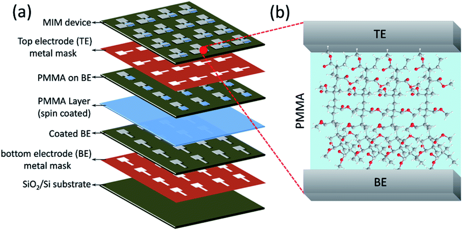 | ||
| Fig. 1 Schematics of the (a) fabrication steps for PMMA-based stacked device, and (b) cross-sectional view of the MIM device; excess polymer film area was wiped out before TE coating. | ||
Results and discussion
Resistive switching characteristics of PMMA-based devices
The current–voltage (I–V) behavior of PMMA-based devices have been investigated with various device configurations. Fig. 2 represents typical I–V plots of four different device configurations, obtained from the first sweep cycle. In all the devices, application of positive bias enables low resistance state (LRS) from high resistance state (HRS) and the process is called as SET. It is well known that, the first SET state corresponds to the initial growth of conducting metal filament between the electrodes, referred to as forming process.39,40 During negative bias, the dissolution of conducting bridge between the electrodes switch the device from LRS to HRS, called as RESET process. In general, the resistive switching characteristics such as SET/RESET voltages, ON/OFF resistance ratio and endurance cycles are greatly influenced by both the device configuration and I–V measurement parameters.41 Especially, the applied potential and compliance current (ICC) range plays crucial role in determining the stable switching operation.41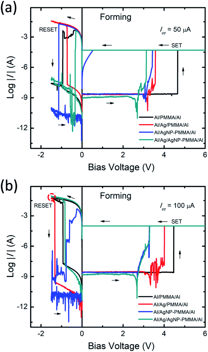 | ||
| Fig. 2 Typical I–V plots of the forming processes of the PMMA-based devices, measured under different ICC ranges (a) 50 μA, and (b) 100 μA. | ||
To elucidate the impact of ICC on resistive switching behavior, the ICC dependent forming processes were initially performed on all the devices. The ICC was varied between 10 μA and 100 μA. In all the devices, smaller ICC range (≤30 μA) exhibited unstable or volatile switching behavior (Fig. S1a and b, ESI†) due to the higher ON resistance (more than 10 kΩ). It is observed that the increase in ICC influences the ON state resistance, interpreting the stability of the conducting filament.42 The increase in ICC revealed stable nonvolatile switching behavior with a decrease of ON resistance value. From the I–V plots (Fig. 2a and b), the ON resistance values are found to be decreased from ∼200 Ω to ∼99 Ω when the ICC varied from 50 μA to 100 μA, respectively. It suggests that, the strong filament formation between the electrodes at higher ICC range,42 enabling large current flow prior to the RESET process (indicated by red dotted circle in Fig. 2b). Therefore, the optimum ICC range required to enable stable resistive switching behavior. Our previous findings also suggested that the ICC range below 10 μA always led to volatile switching due to thinner conductive filament and above this range led to nonvolatile switching due to thicker conductive filament between the electrodes.41 Moreover, the forming voltage of the devices are evaluated from the I–V data of five different cells at each ICC range (Fig. S1c, ESI†). The forming voltage of Al/Ag/AgNP-PMMA/Al device shows smaller value as compared to the remaining device configurations.
In order to understand the repeatable switching behavior of PMMA-based devices, the I–V measurement was carried out for more than 50 continuous sweep cycles, as seen in Fig. 3a–d. In all the cases, the nonvolatile resistive switching is observed though the SET and RESET voltages varied somewhat between the first (black curve) and 50th (red curve) sweep cycles. In the Al/PMMA/Al device (Fig. 3a), the large fluctuations in the SET (1.4 V to 3.9 V) and RESET (−0.15 V to −1.7 V) voltages are found. Especially, the RESET behavior with less prominent HRS (indicated by red double arrow) is observed during reverse biasing. It can be due to the partial rupture of the conducting channels between the electrodes.43 Such partial rupture of the conducting channels affects the next sweep cycle and varies the VSET (indicated by red arrow). However, these fluctuated switching characteristics recovered certainly after few sweep cycles. In the Al/Ag/PMMA/Al device, the long cycle I–V plots show repeatable resistive switching behavior with VSET ranges from 1.8 V to 3.6 V and RESET voltage (VRESET) ranges from −0.28 V to −1.8 V (Fig. 3b). A significant feature of current minimum in the I–V plot is observed during positive biasing (Fig. S2 of ESI†). The current minimum in a logarithmic scale analogous to a zero-current crossing point in a linear scale is associated with electric polarization. The bias voltage at this zero-current crossing point is related with an open-circuit voltage (electromotive force, emf) created by the electrochemical reactions at the electrode–polymer interfaces and distribution of charge carriers in the polymer matrix.44,45 As consequence, electric polarization originates from the accumulation of positive and negative charges at the opposite electrode interfaces. Similar behavior has been found in our previous studies using Ag metal-based polymer resistive switching devices.8,25
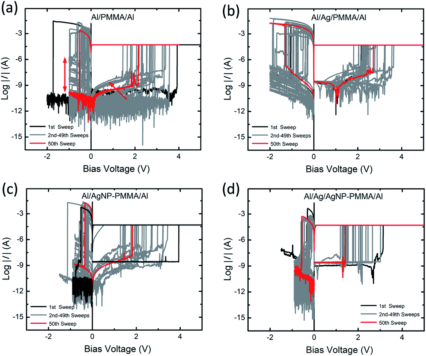 | ||
| Fig. 3 Typical I–V characteristics of (a) Al/PMMA/Al, (b) Al/Ag/PMMA/Al, (c) Al/AgNP-PMMA/Al, and (d) Al/Ag/AgNP-PMMA/Al stacked device, measured at a sweep rate of 5 mV s−1 and ICC of 50 μA for 50 consecutive sweep cycles. | ||
Fig. 3c represents the I–V curves of AgNP included PMMA-based device (Al/AgNP-PMMA/Al). It is found that the VSET is distributed from 1.2 V to 3.9 V and VRESET is varied between −0.16 V and −1.1 V. It is obvious that the inclusion of both Ag electrode and AgNP in the PMMA device (Al/Ag/AgNP-PMMA/Al) exhibited relatively smaller VSET (1.1 V to 3.2 V) and VRESET (−0.09 V to −0.6 V), as seen in Fig. 3d. It can be due to the large Ag+ ionic concentration distributed in the PMMA interface, which favors the SET and RESET operation at smaller biasing voltages for the entire sweep cycles of the Ag/Ag/AgNP-PMMA/Al device.25 These results indicate that the resistive switching characteristics in the PMMA-based devices is altered significantly by the device configuration.
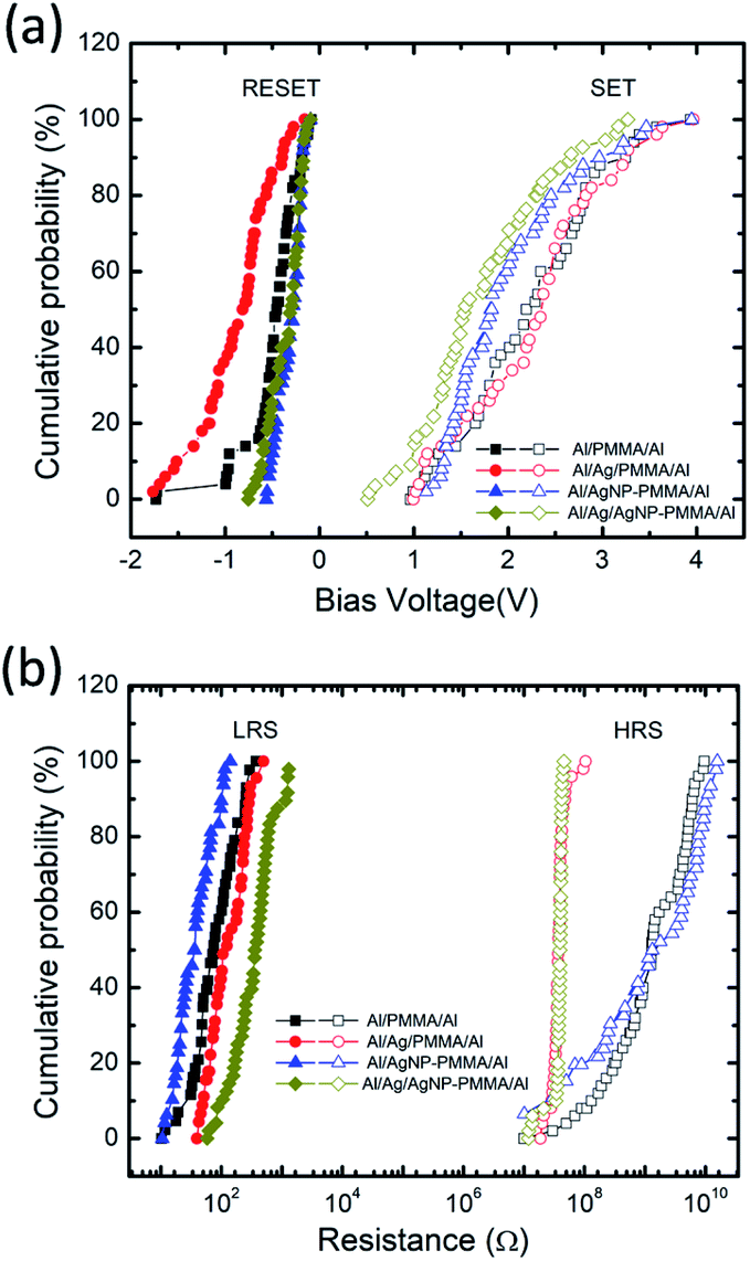
The endurance characteristics of the PMMA-based devices have been analyzed by taking into account of the continuous sweep cycles. Usually, the device configuration and experimental parameters such as stop voltage, step voltage and ICC greatly alters the SET/RESET voltages and ON/OFF resistance ratio.25,41 A statistical distribution of the switching voltages and resistance values are investigated during cycle-to-cycle operation. Fig. 4a and b represents the cumulative probability distributions of VSET/VRESET and resistance states (RLRS/RHRS) for all the devices. The VSET/VRESET were directly extracted from the continuous sweep cycle data (Fig. 3), and the corresponding the resistance values were obtained at ±0.1 V. Table S1 (ESI†) summarizes the mean value (μ) and standard deviation (σ) of the VSET/VRESET and RLRS/RHRS for all the four devices. It is found that the Al/Ag/AgNP-PMMA/Al device exhibits relatively small value of μ and σ in the VSET/VRESET as compared to the remaining device configurations. By using the mean values of RLRS and RHRS, the ON/OFF ratio is found to be ≈107 for Al/PMMA/Al and Al/AgNP-PMMA/Al devices and ≈105 for Al/Ag/PMMA/Al and Al/Ag/AgNP-PMMA/Al devices, respectively.
 | ||
| Fig. 4 Cumulative probability plots of (a) VSET/VRESET behavior, and (b) corresponding RLRS/RHRS of all the four devices, measured using cycle-to-cycle variation. | ||
Filament growth processes in PMMA-based devices
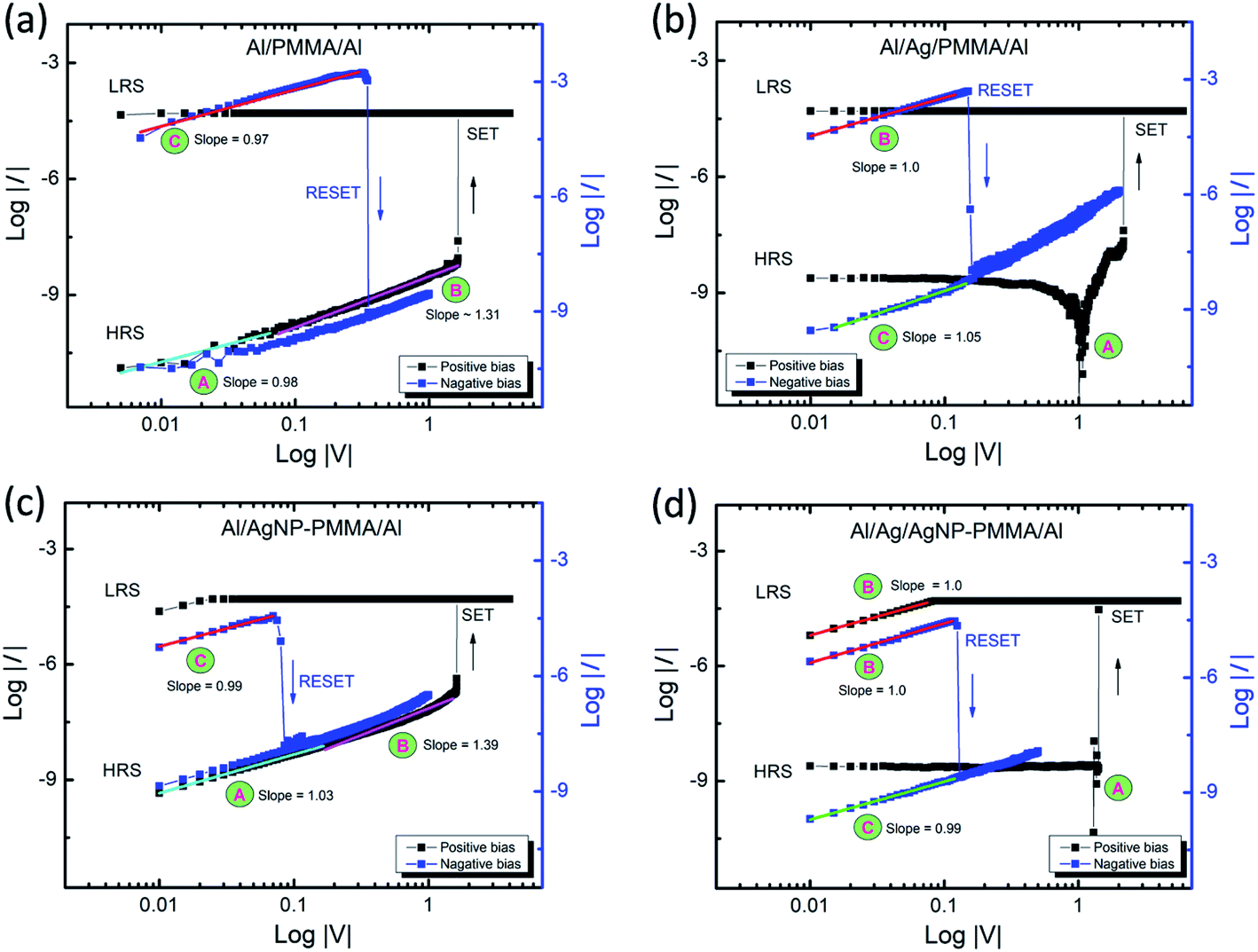
From the I–V measurements, the nonvolatile memory behavior is observed in all the four PMMA-based devices. Nevertheless, each device showed different switching characteristics such as forming voltage, VSET/VRESET and RLRS/RHRS, as shown in Fig. 2–4. It is essential to mention that, the Al/PMMA/Al device showed resistive switching characteristics without an active metal element (Ag) in the device configuration has attracted and stimulated further onto investigate the conduction mechanism of the PMMA-based devices. The I–V curves of both forward and reverse bias conditions were fitted using a double logarithmic plot (log![[thin space (1/6-em)]](https://www.rsc.org/images/entities/char_2009.gif) I–logV) in order to explain the current conduction mechanism in the PMMA-based devices. Fig. 5 illustrates the experimental non-linear I–V plot containing different regions fitted with separate linear slopes, suggesting the variation in conduction phenomena under biasing conditions. It is obvious that the conduction mechanism in PMMA-based devices without Ag electrode is entirely different from the Ag electrode included devices. According to the fitted lines, region A and region B of Al/PMMA/Al and Al/AgNP-PMMA/Al devices (Fig. 5a and c), the ohmic behavior (I ∝ V) with the Mott–Gurney law behavior (I ∝ V2) is observed in the HRS, inferring the charge carrier transport obeys the space charge limited conduction (SCLC) mechanism.46,47 Subsequent to the SET process, ohmic behavior dominates the carrier transport in the LRS (the slope ≈ 1 in the logI–logV of region C), which is a mostly observed characteristics in the conductive metal filament based memory devices.46,48 It is expected that, the Al top electrode oxidized to form partial AlOx layer due to the absorbance of oxygen from the oxygen anions under positive bias, which plays major role in the switching behavior.49,50 The formed AlOx in the electrode may act as the charge trap sites, which can build up a space charge by the accumulation of charge carriers at the electrode–PMMA interface.46,51 Similar Al electrode based resistive switching characteristics governed by SCLC conduction mechanism has already been reported.12,52 Furthermore, the current conduction in the Al/AgNP-PMMA/Al device closely associated with the SCLC conduction mechanism. This can be due to the presence of Al as top electrode in the device architecture, which may induce the charge trap controlled conduction mechanism. However, the presence of Ag element in the polymer matrix in general exhibits the Ag conducting filament based resistive switching.25
I–logV) in order to explain the current conduction mechanism in the PMMA-based devices. Fig. 5 illustrates the experimental non-linear I–V plot containing different regions fitted with separate linear slopes, suggesting the variation in conduction phenomena under biasing conditions. It is obvious that the conduction mechanism in PMMA-based devices without Ag electrode is entirely different from the Ag electrode included devices. According to the fitted lines, region A and region B of Al/PMMA/Al and Al/AgNP-PMMA/Al devices (Fig. 5a and c), the ohmic behavior (I ∝ V) with the Mott–Gurney law behavior (I ∝ V2) is observed in the HRS, inferring the charge carrier transport obeys the space charge limited conduction (SCLC) mechanism.46,47 Subsequent to the SET process, ohmic behavior dominates the carrier transport in the LRS (the slope ≈ 1 in the logI–logV of region C), which is a mostly observed characteristics in the conductive metal filament based memory devices.46,48 It is expected that, the Al top electrode oxidized to form partial AlOx layer due to the absorbance of oxygen from the oxygen anions under positive bias, which plays major role in the switching behavior.49,50 The formed AlOx in the electrode may act as the charge trap sites, which can build up a space charge by the accumulation of charge carriers at the electrode–PMMA interface.46,51 Similar Al electrode based resistive switching characteristics governed by SCLC conduction mechanism has already been reported.12,52 Furthermore, the current conduction in the Al/AgNP-PMMA/Al device closely associated with the SCLC conduction mechanism. This can be due to the presence of Al as top electrode in the device architecture, which may induce the charge trap controlled conduction mechanism. However, the presence of Ag element in the polymer matrix in general exhibits the Ag conducting filament based resistive switching.25
 | ||
| Fig. 5 The experimental and fitted I–V curves of (a) Al/PMMA/Al, (b) Al/Ag/PMMA/Al, (c) Al/AgNP-PMMA/Al, and (d) Al/Ag/AgNP-PMMA/Al devices in the double logarithmic scale under both SET (positive bias) and RESET (negative bias) processes. | ||
Interestingly, the Ag electrode included PMMA-devices exhibit different conducting mechanism from the other two devices, as shown in Fig. 5b and d. Almost similar I–V behavior is observed for both Al/Ag/PMMA/Al and Al/Ag/AgNP-PMMA/Al devices. In the logI–logV plots, three major regions are noticed. The region A in the plot corresponds to the electric polarization effect, which is a most commonly observed behavior in the polymer based ECM cells.8,25 The regions B and C (slope ≈ 1.0) denotes the carrier transportation strays from the ohmic conduction mechanism in the LRS and HRS, respectively.
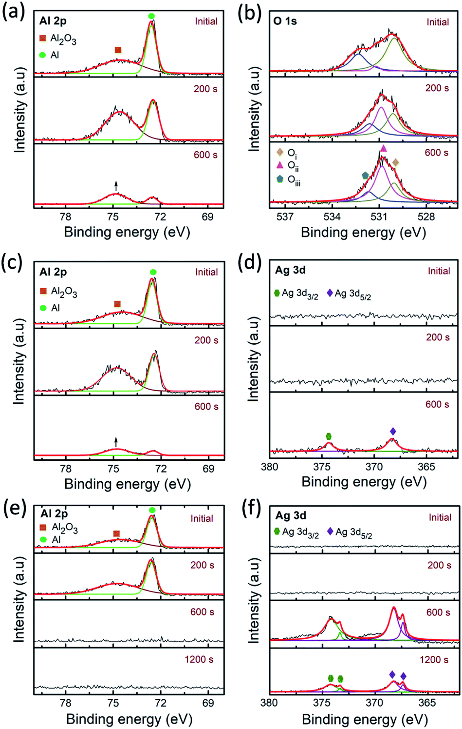
To get further insight into the filament growth processes and resistive switching behavior in the PMMA-based devices, the depth-profiling XPS analysis was conducted. It explains the variation of chemical bonding states of the films on different electrode/electrolyte combinations in the device geometry. Fig. 6a–f illustrates the depth-profiling XPS spectra and their deconvolution (Lorentzian–Gaussian) fittings of the Al 2p, O 1s and Ag 3d signals in the PMMA-based devices. Note that, all the XPS spectra were calibrated with reference to the adventitious C 1s peak at 284.5 eV. Fig. 6a and b represents the Al 2p, O 1s signals of the Al/PMMA/Al device after enabling the LRS under forward biasing. The observed Al 2p signals were fitted with two deconvolution peaks of 72.5 eV and 74.7 eV, corresponding to the Al–Al bonding and Al–O bonding of the Al2O3, respectively.53 It is observed that, the area ratio of the Al–O peak to the Al–Al peak increases over sputter-etching times. In particular, the area of Al–O peak increased (marked with up arrow) almost four times higher than the Al–Al peak at 600 s. It demonstrates that the Al atoms from the electrode combine with PMMA at the Al/PMMA interface can give rise to the formation of AlOx due to the capture of O atoms from PMMA. Furthermore, the observation of small Al 2p signals at the Al/PMMA interface (at 600 s) can be because of the expansion of the interfacial layer.54
 | ||
| Fig. 6 Depth-profiling XPS spectra of Al 2p, O 1s and Ag 3d signals of (a) and (b) Al/PMMA/Al (c) and (d) Al/AgNP-PMMA/Al, and (e) and (f) Al/Ag/PMMA/Al devices after biasing in LRS, respectively. | ||
The O 1s XPS spectra in Fig. 6b is fitted with three deconvolution peaks located at 530.1 eV (Oi), 531.2 eV (Oii), and 532.3 eV (Oiii).54 The low binding energy component Oi is ascribed to the formation of Al–O by the O2− bound to the oxidized Al.55,56 The medium binding energy component Oii is attributed to the oxygen vacancies ( ).57,58 The high binding energy component Oiii is mainly due to the O–H groups of the surface adsorbed H2O.59 In the initial stage of O 1s spectra, the Oi component appears to predominate near the surface of Al electrode and decreases further to the Al/PMMA interface. As the Oi peak decreases, the area ratio of the Oii peak is anticipated to increase noticeably. The area of Oiii peak related to surface O–H group is decreased with an increase in depth. It is also observed that the Oiii and Oii peaks are negatively shifted when the sputter-etching increases, which is mostly due to the electronic interaction between the out-diffused Al atoms and PMMA polymer.60 The variation of O 1s bonding states as function of sputter-etching times are in good agreement with the existence of rich AlOx layer and
  in the interfacial regime (Fig. 6b). It thus confirms that the formation of
  as conducting channel between the electrodes under LRS.
To further clarify the presence of AlOx layer and  in the HRS of the device, the depth-profiling XPS scans were also conducted on the Al/PMMA/Al device under pristine state. Fig. S3a and b (ESI†) represents the Al 2p, O 1s signals of the pristine Al/PMMA/Al device. From the Al 2p XPS spectra, it is obvious that intensity of the Al–Al component is substantially higher than Al–O component. Upon the increase in depth, a slight increase in Al–O component is found that may be due to the occurrence of small stoichiometric changes in the Al layer.54 Though, the O 1s spectra evidences almost similar peak profiles in the entire depth-profiling studies. The Oi peak correspond to the Al–O bonding appeared to be similar from the surface to the interface. The peak area of Oiii decreases with an increase in sputter-etching time. It is obvious that the area of the Oii peak is much smaller than both Oi and Oiii peaks. This is consistent with the insignificant composition of
  and AlOx layer available in the interfacial region under HRS of the pristine device.54
To understand the influence of Ag element on the PMMA device configuration, both AgNP included PMMA and Ag electrode included PMMA devices were also used for depth-profiling XPS analysis. Fig. 6c and d represents the XPS spectra of the Al 2p and Ag 3d signals of the Al/AgNP-PMMA/Al device, respectively. From the Al 2p spectra, it is obvious that the Al–Al component is prominent than the Al–O component in the initial layer. The increase in depth reveals that the increase in area ratio of the Al–O peak to the Al–Al peak. The higher Al–O peak area (marked with up arrow) than the Al–Al peak area is found at 600 s, which indicates the formation of AlOx layer in the interface. The corresponding O 1s spectra (Fig. S4 of ESI†) also illustrates the existence of strong Oi and Oii components than the Oiii component. A slight shift in the peak position is found in the O 1s spectrum while the etch depth increases, that can be due to the interaction between Al and O in the Al/PMMA interfacial region. Essentially, the simultaneous detection of Al 2p and Ag 3d signals at 600 s implies the existence of substoichiometric interfacial layers comprising AlOx and Ag in the expanded Al/PMMA interfacial region.54 However, the disappearing trend in Al 2p signal and the emerging trend in Ag 3d signal is observed beyond 600 s. The Ag 3d peak arises majorly because of the existence of pre-dissolved AgNP in the PMMA polymer matrix. Fig. 6d shows the Ag 3d XPS spectra of the Al/AgNP-PMMA/Al device. It can be seen that the Ag 3d spectra consists of two major peaks at 368.1 eV and 374.1 eV, corresponding to the Ag 3d5/2 and Ag 3d3/2 binding energies of metallic Ag (Ag0), respectively.61–63 As can be seen in Fig. S5 of ESI,† where the Ag 3d doublet peaks are observed after sputter-etching of 600 s, a slight shift in the peak position and change in FWHM is found. According to Busby et al.,64 this phenomenon can be ascribed to the occurrence of metallic nanoparticle with different particle sizes. The AgNP with smaller diameter mostly exhibit the shift toward higher binding energies. This confirms the formation of Ag conducting metallic bridge between the electrodes with distributed Ag nanoclusters in the interfaces of Al/AgNP-PMMA/Al device.
Fig. 6e and f illustrates the Al 2p and Ag 3d signals of the Ag electrode included PMMA device (Al/Ag/PMMA/Al). It is obvious that the depth-profile exhibits the prominent Al–Al peak with negligibly small Al–O peak. At 600 s, the Al 2p signal is disappeared and Ag 3d signal is emerged, representing the origin of second electrode layer of the device. The binding energies of the Ag 3d5/2 doublet peak located at 367.3, eV and 368.1 eV and Ag 3d3/2 doublet peak found at 373.3 eV and 374.1 eV after 600 s of depth-profiling studies.65 Thereby, it explains the presence of more than one silver species such as metallic Ag and oxidized Ag in the interfaces. It was also estimated that, approximately 94% of metallic silver is present during electrode region. The increase in depth to interfacial regime reduces the metallic silver (∼91%) and enhances the oxidized silver concentration.65 This can be due to the interaction between the Ag atom from electrode and O atom from the PMMA polymer. Observation of the decrease in overall intensity of Ag 3d signals from 600 s to 1200 s is mainly because of the variation of electrode region to interfacial region. The corresponding O 1s XPS spectra of the device is shown in Fig. S6 of ESI.† The Oi, Oii and Oiii components almost similar till 600 s of sputter-etching. At 1200 s, a large downshift in the peak positions and change in peak intensity suggests that the change in stoichiometry from electrode to interfacial region.55 In particular, the increase in Oii component can be due to the formation of AgO that may create the oxygen deficiencies in the interfaces.66
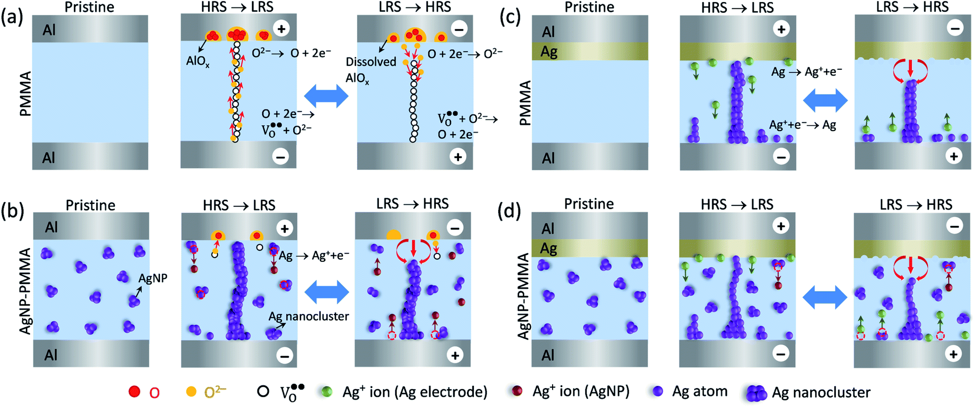
On the basis of the I–V characteristics and XPS results, we propose the resistive switching mechanism in the PMMA-based devices, as schematically shown in Fig. 7. In the Al/PMMA/Al device, formation of rich AlOx layer in the interfacial region suggests that the resistive switching behavior is associated with the valence change mechanism (VCM).18,19 Since VCM cell operates by the formation of oxygen vacancies ( ) as conducting bridge between the electrodes under positive biasing, whereas the recombination of oxygen vacancies and oxygen ions (O2−) under negative biasing ruptures the conducting bridge (Fig. 7a). The depth-profiling XPS results reveal that the presence of AlOx in the active region by the interfacial interaction between Al electrode and PMMA in the Al/PMMA/Al device under biasing. In particular, presence of oxygen atoms in the PMMA can able to react with the out-diffused Al atoms due to the higher oxygen concentration gradient in the interface and higher oxidation tendency of Al.54,67 It is thus forms the AlOx layer under positive biasing and act as charge trap sites, demonstrating the SCLC mechanism. But, in the case of the Al/AgNP-PMMA/Al device, the resistive switching arises by the electrochemical redox process of the pre-dissolved Ag nanoparticles (AgNP) in the PMMA matrix (Fig. 7b). Under positive bias condition, some of the Ag atoms from AgNP can be oxidized near the positive electrode and migrates Ag+ ions into the counter electrode. These Ag+ ion migration via PMMA can give two possibilities, (1) it can reduce at the counter electrode (Ag+ + e− → Ag) and grows the Ag filament towards anode, (2) the reduction process happens at the distributed AgNP in the PMMA interface before reaching to counter electrode, which enlarges the AgNP to Ag nanoclusters.68,69 As consequence, the pre-existing AgNP in the PMMA matrix can able to form a metallic bridge between the electrodes with distributed Ag nanoclusters in the interfaces, which enables nonvolatile memory behaviour. Observation of minimum ON state resistance and nonvolatile resistive switching behavior in the Al/AgNP-PMMA/Al device suggests that the resistive switching arises mainly due to the formation of continuous conducting channels. The depth-profiling XPS scans confirm the presence of Ag 3d element in the Al/PMMA interfacial region, which is in agreement with the continuous conducting channel formation between the electrodes. It is also evidenced that, the Al as top electrode used in this device configuration forms a partial AlOx layer near the Al/PMMA region, which may influence the trap-controlled current conduction.
 | ||
| Fig. 7 Schematic illustration of the proposed switching mechanisms for (a) Al/PMMA/Al, (b) Al/AgNP-PMMA/Al, (c) Al/Ag/PMMA/Al, and (d) Al/Ag/AgNP-PMMA/Al devices under biasing conditions. | ||
Fig. 7c and d illustrates the schematics of the switching mechanism in the Ag electrode included PMMA-based devices. For the Al/Ag/PMMA/Al device, the Ag+ ions supplied from the Ag top electrode (TE) alone contribute to the filament formation. Under positive bias condition, this Ag+ ions migrate toward the Al bottom electrode (BE), and forms the Ag bridge between the electrodes. Especially, the filament growth takes place at different sites based on the concentration of Ag+ ions in the interface.41 By taking into account of the I–V characteristics of the Al/Ag/PMMA/Al device, large positive voltage always needed to SET the device. It indicates that, less Ag+ ion concentration in the PMMA interface causes higher VSET. Significantly, the inclusion of both Ag electrode and AgNP in the PMMA device (Al/Ag/AgNP-PMMA/Al) enables lower VSET as compared to the remaining devices. It indicates that, the Ag+ ions injected from both the oxidized Ag TE and pre-dissolved AgNP in the PMMA matrix contribute to the filament growth. Presence of two Ag source in the device configuration can supply large concentration of Ag+ ions in the interface, which potentially favours the filament formation and resistive switching characteristics. These results conclude that the combinations of electrode/electrolyte arrangement in the MIM device structure can be able to alter the resistive switching behavior by different conduction mechanism. As a result, the Al/PMMA/Al device exhibits the coexistence of ohmic, Mott–Gurney law and a sudden increase in current regions corresponding to SCLC behavior, which is in contrast to the observation of electric polarization effect and ohmic conduction behavior in the Ag electrode included devices.
Conclusions
In summary, we demonstrated the resistive switching characteristics and conduction mechanism in the PMMA-based devices with different electrode/electrolyte configurations. From I–V studies, the ICC range above 50 μA exhibits nonvolatile switching and below this range shows volatile switching behavior in all the four devices. The resistive switching characteristics and conduction mechanism in PMMA-based devices significantly altered when the Al as top electrode is present in the device configuration. The depth-profiling XPS results evidence the formation of AlOx in the interfacial region of the Al/PMMA/Al device due to the capture of O atoms from PMMA. Thereby, it confirms the formation of oxygen vacancies as conducting bridge between the electrodes, enabling switching operation. Whereas, the incorporation of Ag element in the PMMA-based device exhibits resistive switching by the metallic Ag filament between the electrodes, interpreting the ohmic behavior in the current conduction. These results contribute toward to understand the importance of device configuration on the resistive switching characteristics of the polymer based MIM devices.Experimental
Materials and methods
Similar steps were adopted to fabricate the Al/Ag/PMMA/Al, Al/AgNP-PMMA/Al and Al/Ag/AgNP-PMMA/Al devices. For Al/Ag/PMMA/Al device, the Ag as TE with a thickness of ∼60 nm was coated before coating Al (as protect layer) using thermal evaporation method. In Al/AgNP-PMMA/Al device, the silver nanoparticle (AgNP) with an average particle size of ∼15 nm was used as received (SRL chemicals, India). For the AgNP-PMMA film, 2 wt% of AgNP was additionally incorporated into the PMMA solution, and the remaining procedures were same as mentioned above for film preparation. Owing to the high surface energy of the nanoparticles, there is possibility to agglomerate the AgNP. Hence, the AgNP was ultra-sonicated (∼30 min) before adding into PMMA solution. In the Al/Ag/AgNP-PMMA/Al, the Ag as TE and AgNP incorporated PMMA as electrolyte was used. It is essential to mention that, the constant PMMA film thickness was maintained in all the devices. The polymer film thickness was estimated to be ∼200 nm using atomic force microscopy. Fig. S7 (ESI†) represents the surface topography of the prepared PMMA film.
Characterization
The current–voltage (I–V) measurements were performed using a semiconductor characterization system (Keithley 4200A-SCS) equipped with a home-made probe station setup. The I–V measurements were carried out at room temperature and atmospheric conditions. In the entire I–V measurements, a constant dual sweep mode was performed for both positive and negative biases. During I–V study, the positive bias voltage was applied to the TE and swept with constant sweep rate (5 mV s−1), whereas the BE was grounded. In our study, the compliance current (ICC) was fixed only for the positive bias in order to regulate the ON state current, though the negative bias was swept without fixing certain ICC range. The thickness of PMMA film was estimated using AFM (SII E-Sweep/NanoNavi II, in the non-contact mode). The depth-profiling X-ray photoelectron spectroscopy (XPS, ESCALAB 250Xi, Thermo Scientific) was carried out on the PMMA-based MIM devices, which is essential to understand the layer-by-layer chemical bonding states in the electrode and electrolyte regions. For measurement, the depth-profiling scans were done on the device junction area with sputter-etching varied at a rate of ∼0.10 nm s−1.Conflicts of interest
There are no conflicts to declare.Acknowledgements
Dr KK would like to thank Science and Engineering Research Board (SERB) and Department of Science & Technology (DST), India to carry out this work under early career research (ECR/2017/002615) and DST inspire faculty scheme (DST/INSPIRE/04/2016/000246). Authors would like to thank Mr Kennedy Jeevarathinam for his support to take the XPS measurement from the central instrumentation facility.Notes and references
- R. Waser and M. Aono, Nat. Mater., 2007, 6, 833–840 CrossRef CAS PubMed.
- D. H. Kwon, K. M. Kim, J. H. Jang, J. M. Jeon, M. H. Lee, G. H. Kim, X. S. Li, G. S. Park, B. Lee, S. Han, M. Kim and C. S. Hwang, Nat. Nanotechnol., 2010, 5, 148–153 CrossRef CAS PubMed.
- G. Milano, F. F. Lupi, M. Fretto, C. Ricciardi, N. De and L. Boarino, Adv. Quantum Technol., 2020, 2000009, 1–9 Search PubMed.
- R. Ge, X. Wu, M. Kim, J. Shi, S. Sonde, L. Tao, Y. Zhang, J. C. Lee and D. Akinwande, Nano Lett., 2018, 18, 434–441 CrossRef CAS PubMed.
- Q. Cui, M. Sakhdari, B. P. Chamlagain, H.-J. Chuang, Y. Liu, M. M.-C. Chen, Z. Zhou and P.-Y. Chen, ACS Appl. Mater. Interfaces, 2016, 8(50), 34552–34558 CrossRef CAS PubMed.
- S. Wu, T. Tsuruoka, K. Terabe, T. Hasegawa, J. P. Hill, K. Ariga and M. Aono, Adv. Funct. Mater., 2011, 21, 93–99 CrossRef CAS.
- Y. Li, C. Zhang, Z. Li, P. Gu, Z. Wang, H. Li, J. Lu and Q. Zhang, J. Mater. Chem. C, 2019, 7, 3512–3521 RSC.
- K. Krishnan, M. Aono and T. Tsuruoka, J. Mater. Chem. C, 2018, 6, 6460–6464 RSC.
- W.-J. Joo, T.-L. Choi, K.-H. Lee and Y. Chung, J. Phys. Chem. B, 2007, 111, 7756–7760 CrossRef CAS PubMed.
- T. Tsuruoka, T. Hasegawa, K. Terabe and M. Aono, Nanotechnology, 2012, 23, 435705 CrossRef PubMed.
- X. Tian, S. Yang, M. Zeng, L. Wang, J. Wei, Z. Xu, W. Wang and X. Bai, Adv. Mater., 2014, 26, 3649–3654 CrossRef CAS PubMed.
- D.-C. Hu, R. Yang, L. Jiang and X. Guo, ACS Appl. Mater. Interfaces, 2018, 10, 6463–6470 CrossRef CAS PubMed.
- R. Zazpe, M. Ungureanu, F. Golmar, P. Stoliar, R. Llopis, F. Casanova, D. F. Pickup, C. Rogero and L. E. Hueso, J. Mater. Chem. C, 2014, 2, 3204–3211 RSC.
- T. S. Lee, N. J. Lee, H. Abbas, H. H. Lee, T.-S. Yoon and C. J. Kang, ACS Appl. Electron. Mater., 2020, 2, 1154–1161 CrossRef CAS.
- Y. Li, Q. Qian, X. Zhu, Y. Li, M. Zhang, J. Li, C. Ma, H. Li, J. Lu and Q. Zhang, InfoMat, 2020, 2, 995–1033 CrossRef CAS.
- C. Chen, S. Gao, G. Tang, H. Fu, G. Wang, C. Song, F. Zeng and F. Pan, ACS Appl. Mater. Interfaces, 2013, 5, 1793–1799 CrossRef CAS PubMed.
- R. Waser, R. Dittmann, C. Staikov and K. Szot, Adv. Mater., 2009, 21, 2632–2663 CrossRef CAS.
- J.-Y. Chen, C.-W. Huang, C.-H. Chiu, Y.-T. Huang and W.-W. Wu, Adv. Mater., 2015, 27, 5028–5033 CrossRef CAS PubMed.
- M.-C. Wu, Y.-H. Ting, J.-Y. Chen and W.-W. Wu, Adv. Sci., 2019, 1902363 CrossRef CAS PubMed.
- G. Milano, S. Porro, I. Valov and C. Ricciardi, Adv. Electron. Mater., 2019, 1800909 CrossRef.
- K. Maas, E. Villepreux, D. Cooper, E. Salas-colera, J. Rubio-zuazo, G. R. Castro, O. Renault, C. Jimenez, H. Roussel, X. Mescot, Q. Rafhay, M. Boudard and M. Burriel, Adv. Funct. Mater., 2020, 30, 1909942 CrossRef CAS.
- I. Valov, R. Waser, J. R. Jameson and M. N. Kozicki, Nanotechnology, 2011, 22, 254003 CrossRef PubMed.
- S. Menzel, S. Tappertzhofen, R. Waser and I. Valov, Phys. Chem. Chem. Phys., 2013, 15, 6945–6952 RSC.
- H. Lv, X. Xu, H. Liu, R. Liu, Q. Liu, W. Banerjee, H. Sun, S. Long, L. Li and M. Liu, Sci. Rep., 2015, 5, 1–6 Search PubMed.
- K. Krishnan, T. Tsuruoka, C. Mannequin and M. Aono, Adv. Mater., 2016, 28, 640–648 CrossRef CAS PubMed.
- S.-H. Lee, H.-L. Park, M.-H. Kim, S. Kang and S.-D. Lee, ACS Appl. Mater. Interfaces, 2019, 11, 30108–30115 CrossRef CAS PubMed.
- Y. Yang, P. Gao, S. Gaba, T. Chang, X. Pan and W. Lu, Nat. Commun., 2012, 3, 732–738 CrossRef PubMed.
- B. K. You, W. I. Park, J. M. Kim, K.-I. Park, H. K. Seo, J. Y. Lee, Y. S. Jung and K. J. Lee, ACS Nano, 2014, 8, 9492–9502 CrossRef CAS PubMed.
- H. He and N. J. Tao, Adv. Mater., 2002, 14, 161–164 CrossRef CAS.
- R. Berndt, J. Kröger, N. Néel and G. Schull, Phys. Chem. Chem. Phys., 2010, 12, 1022–1032 RSC.
- A. Mehonic, A. Vrajitoarea, S. Cueff, S. Hudziak, H. Howe, C. Labbé, R. Rizk, M. Pepper and A. J. Kenyon, Sci. Rep., 2013, 3, 2708 CrossRef CAS PubMed.
- A. Younis, D. Chu and S. Li, J. Mater. Chem. C, 2014, 2, 10291–10297 RSC.
- C. Hu, M. D. McDaniel, A. Posadas, A. A. Demkov, J. G. Ekerdt and E. T. Yu, Nano Lett., 2014, 14, 4360–4367 CrossRef CAS PubMed.
- K. Krishnan, M. Muruganathan, T. Tsuruoka, H. Mizuta and M. Aono, Adv. Funct. Mater., 2017, 27, 1605104 CrossRef.
- P. K. Sarkar, S. Bhattacharjee, M. Prajapat and A. Roy, RSC Adv., 2015, 5, 105661–105667 RSC.
- G. Sahoo, N. Sarkar, D. Sahu and S. K. Swain, RSC Adv., 2017, 7, 2137–2150 RSC.
- O. Bohnke, G. Frand, M. Rezrazi, C. Rousselot and C. Truche, Solid State Ionics, 1993, 66, 97–104 CrossRef CAS.
- H.-W. Chen, T.-P. Lin and F.-C. Chang, Polymer, 2002, 43, 5281–5288 CrossRef CAS.
- T. Tsuruoka, K. Terabe, T. Hasegawa and M. Aono, Nanotechnology, 2010, 21, 425205 CrossRef CAS PubMed.
- C. W. Hsu and L. J. Chou, Nano Lett., 2012, 12, 4247–4253 CrossRef CAS PubMed.
- K. Krishnan, M. Aono and T. Tsuruoka, Nanoscale, 2016, 8, 13976–13984 RSC.
- S. La Barbera, D. Vuillaume and F. Alibart, ACS Nano, 2015, 9, 941–949 CrossRef CAS PubMed.
- S. Ge, Y. Wang, Z. Xiang and Y. Cui, ACS Appl. Mater. Interfaces, 2018, 10, 24620–24626 CrossRef CAS PubMed.
- I. Valov, E. Linn, S. Tappertzhofen, S. Schmelzer, J. van den Hurk, F. Lentz and R. Waser, Nat. Commun., 2013, 4, 1771 CrossRef CAS PubMed.
- S. Tappertzhofen, I. Valov, T. Tsuruoka, T. Hasegawa, R. Waser and M. M. Aono, ACS Nano, 2013, 7, 6369 CrossRef PubMed.
- E. W. Lim and R. Ismail, Electronics, 2015, 4, 586–613 CrossRef CAS.
- K. Zhou, G. Ding, C. Zhang, Z. Lv, S. Luo, Y. Zhou, L. Zhou, X. Chen, H. Li and S. T. Han, J. Mater. Chem. C, 2019, 7, 843–852 RSC.
- X. Guo, J. Liu, L. Cao, Q. Liang and S. Lei, ACS Omega, 2019, 4, 10419–10423 CrossRef CAS PubMed.
- A. Kumar, M. Das, V. Garg, B. S. Sengar, M. T. Htay, S. Kumar, A. Kranti and S. Mukherjee, Appl. Phys. Lett., 2017, 110, 253509 CrossRef.
- X.-F. Cheng, Y. Zhao, W. Ye, C. Yu, J.-H. He, F. Y. Wang and J.-M. Lu, J. Mater. Chem. C, 2020, 8, 2964–2969 RSC.
- S. Liu, X. Chen and G. Liu, Polym. Int., 2021, 70, 374–403 CrossRef CAS.
- S. K. Hwang, J. M. Lee, S. Kim, J. S. Park, H. Il Park, C. W. Ahn, K. J. Lee, T. Lee and S. O. Kim, Nano Lett., 2012, 12, 2217–2221 CrossRef CAS PubMed.
- J. F. Moulder, W. F. Stickle, P. E. Sobol and K. D. Bomben, Handbook of X-ray Photoelectron Spectroscopy, Physical Electronic Inc., Eden Prairie, MN, 1995 Search PubMed.
- C. J. Park, S. W. Han and M. W. Shin, ACS Appl. Mater. Interfaces, 2020, 12(28), 32131–32142 CrossRef CAS PubMed.
- R.-C. Fang, Q.-Q. Sun, P. Zhou, W. Yang, P.-F. Wang and D. W. Zhang, Nanoscale Res. Lett., 2013, 8, 92 CrossRef PubMed (1–7)..
- S. K. Vishwanath, H. Woo and S. Jeon, Nanotechnology, 2018, 29, 235202 CrossRef PubMed.
- M. Chen, X. Wang, Y. H. Yu, Z. L. Pei, X. D. Bai, C. Sun, R. F. Huang and L. S. Wen, Appl. Surf. Sci., 2000, 158, 134–140 CrossRef CAS.
- S. Baek, J. Song and S. Lim, Phys. B, 2007, 399, 101–104 CrossRef CAS.
- M. Jongsun, H. Sungho, J. Gunho, C. Minhyeok, K. Seonghyun, H. Hyunsang and L. Takhee, Nanotechnology, 2009, 20, 095203 CrossRef PubMed.
- J.-L. Lan, S.-J. Cherng, Y.-H. Yang, Q. Zhang, S. Subramaniyan, F. S. Ohuchi, S. A. Jenekhe and G. Cao, J. Mater. Chem. A, 2014, 2, 9361–9370 RSC.
- C. Y. Dong, D. S. Shang, L. Shi, J. R. Sun, B. G. Shen, F. Zhuge, R. W. Li and W. Chen, Appl. Phys. Lett., 2011, 98, 072107 CrossRef.
- I. Roppolo, M. Castellino, K. Bejtka, G. Rizza, D. Perrone, P. Coulon, A. Chiappone, K. Rajan, S. Bocchini, C. Ricciardi, C. F. Pirri and A. Chiolerio, J. Phys. Chem. C, 2017, 121, 14285–14295 CrossRef CAS.
- N. Feng, Q. Wang, A. Zheng, Z. Zhang, J. Fan, S.-B. Liu, J.-P. Amoureux and F. Deng, J. Am. Chem. Soc., 2013, 135, 1607–1616 CrossRef CAS PubMed.
- Y. Busby and J. J. Pireaux, J. Electron Spectrosc. Relat. Phenom., 2014, 192, 13–18 CrossRef CAS.
- K. Rajan, S. Bocchini, A. Chiappone, I. Roppolo, D. Perrone, M. Castellino, K. Bejtka, M. Lorusso, C. Ricciardi, C. F. Pirri and A. Chiolerio, Flexible Printed Electron., 2017, 2, 024002 CrossRef.
- F. M. Simanjuntak, T. Ohno and S. Samukawa, ACS Appl. Electron. Mater., 2019, 1, 18–24 CrossRef CAS.
- D. R. Gaskell, Introduction to the Thermodynamics of Materials, Taylor & Francis, New York, 4th edn, 2003, ch. 12 Search PubMed.
- Y. Yang, B. Chen and W. D. Lu, Adv. Mater., 2015, 27, 7720–7727 CrossRef CAS PubMed.
- Y. Sun, C. Song, S. Yin, L. Qiao, Q. Wan, J. Liu, R. Wang, F. Zeng and F. Pan, ACS Appl. Mater. Interfaces, 2020, 12, 29481–29486 CAS.
Footnote |
| † Electronic supplementary information (ESI) available. See DOI: 10.1039/d1ra03561d |
| This journal is © The Royal Society of Chemistry 2021 |