
 Open Access Article
 This Open Access Article is licensed under a Creative Commons Attribution-Non Commercial 3.0 Unported Licence
Lifetime elongation of quantum-dot light-emitting diodes by inhibiting the degradation of hole transport layer†
Bo-Yen Lin a,
Wen-Chen Dingb,
Chia-Hsun Chenb,
Ya-Pei Kuoc,
Jiun-Haw Lee*b,
Chun-Yu Lee*c and
Tien-Lung Chiu*a
a,
Wen-Chen Dingb,
Chia-Hsun Chenb,
Ya-Pei Kuoc,
Jiun-Haw Lee*b,
Chun-Yu Lee*c and
Tien-Lung Chiu*a
aDepartment of Electrical Engineering, Yuan Ze University, Taoyuan 32003, Taiwan. E-mail: tlchiu@saturn.yzu.edu.tw
bGraduate Institute of Photonics and Optoelectronics, Department of Electrical Engineering, National Taiwan University, Taipei 10617, Taiwan. E-mail: jiunhawlee@ntu.edu.tw
cAU Optronics Corporation, Hsinchu 30010, Taiwan. E-mail: d01941010@ntu.edu.tw
First published on 11th June 2021
Abstract
Developing a colloidal quantum-dot light-emitting device (QDLED) with high efficiency and good reliability is necessarily preliminary for the next-generation high-quality display application. Most QDLED reports are focused on efficiency improvement, but the device operational lifetime issue is less addressed and also the relevant degradation mechanisms. This study achieved a 1.72 times elongation in the operational lifetime and a 9 times improvement in the efficiency of QDLED by inserting a hole-transporting/electron-blocking poly(9-vinylcarbazole) (PVK) layer, which prevented operational degradation on poly[(9,9-dioctylfluorenyl-2,7-diyl)-co-(4,4′-(N-(4-secbutylphenyl))-diphenylamine)] (TFB) hole-transporting layer and also confined the electron in the QD-emitting layer. Although the TFB/PVK HTL structure is a well-known pair to enhance the device performance, its detailed mechanisms were rarely mentioned, especially for relative operational lifetime issues. Herein, a new insight behind operational lifetime elongation of QDLED is disclosed through various fundamental experiments including steady-state photoluminescence, transient electroluminescence and single-carrier only devices. Evidently, other than QD degradation, this study found that the other crucial factor that decreased the device lifetime was TFB-HTL degradation using steady-state photoluminescence and transient electroluminescence analyses. The PVK electron-only device exhibited a stable voltage value when it was driven by fixed current, which also affirmed that PVK has excellent electron-stability characteristics.
Introduction
Colloidal quantum dots (QDs) have been widely investigated due to their attractive characteristics, such as high photoluminescence quantum yield, low driving voltage, narrow full width at half maximum of the emission spectra, high color purity, tunable emission color, and cost-effective fabrication.1–10 These characteristics make QDs potential electroluminescence (EL) material in quantum-dot light-emitting devices (QDLEDs) and a promising candidate for next-generation wide-color-gamut displays and solid-state lighting applications. Depending on the size and composition of QDs, the quantum confinement effect allows them to modulate the emissive color to cover wavelengths ranging from the ultraviolet (UV) region to the near-infrared (NIR) region.11–16 Colvin et al. reported the first QDLED with a polymer–QD bilayer structure, whose external quantum efficiency (EQE) was only 0.001%.17 Since then, considerable efforts have been invested in material synthesis and device architecture and significant progress has been achieved; for example, QDLED performance has been boosted from 0.001% to over 20%. Numerous approaches have been proposed for enhancing QDLED performance, such as the engineering of functional layers, including charge transport or injection layers and electron-blocking layers,18–24 and passivation methods, including positive aging treatment.25,26 One of the challenges faced by highly efficient QDLEDs is the carrier imbalance resulting from the mobility mismatch of the carrier transporting layer. For state-of-the-art QDLEDs, inorganic oxide materials, such as zinc oxide (ZnO), are used as electron transporting layers (ETL) because ZnO facilitates efficient electron injection due to its suitable energy-level alignment in QDs. By contrast, conventional organic materials are used as the hole transporting layer (HTL); thus, the electron mobility of ETL is considerably higher than the hole mobility of HTL. Therefore, excess electrons may accumulate in QDs and transport them across the QD layer to HTL. In this scenario, the electron current leakage can damage HTL and degrade its efficiency. To address this challenge, Peng et al. proposed a highly efficient QDLED with an EQE of 20.5%. They combined inorganic ZnO with an organic HTL to inhibit electron migration for creating carrier balance in the QD layer.18 Furthermore, thanks to the development on HTL architecture, as poly[(9,9-dioctylfluorenyl-2,7-diyl)-co-(4,4′-(N-(4-secbutylphenyl))-diphenylamine)] (TFB)/poly(9-vinylcarbazole) (PVK) have been demonstrated for stepwise hole injection and the increase of hole transport mobility to create carrier injection balance in the QD layer.27 In addition, the operational lifetime and degradation mechanism of QDLEDs are also important challenges in realizing their commercial applications, and inadequate studies have been conducted on these topics.28–31 Aziz et al. reported that excitons are present in HTL under standard driving conditions.31 These excitons originate from electrons that drift across the QD layer into HTL and recombine with holes in it. These excitons can damage organic materials. Therefore, HTL degradation under EL must be considered. The driving approach is an effective method for achieving device stability. To the best of our knowledge, the operational lifetime of an organic light-emitting device (OLED) is different under direct current (DC) and pulse current (PC) driving. A longer operational lifetime is achieved under PC driving than under DC driving, which is attributed to the reduction of the ionic organic material present in OLED.32In this study, we manufactured a QDLED exhibiting higher efficiency and a longer operational lifetime by introducing a hole transporting/electron-blocking layered pair, TFB/PVK, relative to the TFB device (without PVK). Although TFB/PVK pair is typically used to facilitate the hole injection and transport for raising device performance, in the current study the main contribution of PVK is in charge of the electron confinement inside the QD layer to improve the carrier balance for high efficiency and to inhibit material degradation for elongating the operational lifetime of QDLEDs. Surprisingly, the degradation mechanism of the TFB device was determined and it mainly originates not only from QDs but also TFB degradation, which was confirmed from transient electroluminescence (TREL) and steady-state photoluminescence (PL) analyses. The insertion of PVK at the interface of TFB and QDs layers plays a crucial role and significantly affects the efficiency and operational lifetime in QDLEDs because it has excellent electron-confinement ability and material stability against electrons than TFB does. That was proven through a test of observing the voltage variation of electron-only devices (EOD) over time under a constant current driving.
Experimental
Fabrication of QDLED
A QDLED was fabricated using the all-solution process. The TFB/PVK device had the following structure: indium tin oxide (ITO)/hole injection layer (HIL)/first HTL/second HTL/emitting layer (EML)/ETL/Al, where poly(3,4-ethylenedioxythiophene)–poly(styrenesulfonate) (PEDOT:PSS) was used as the HIL. TFB, which is a common organic hole transporting material, was used as the first HTL, and PVK was used as the second HTL. QDs composed of CdZnSeS/ZnS/OT with a particle size of 10.5 nm and a photoluminescence (PL) quantum yield of approximately 85% were used as the emitting layer. In addition, ZnO nanoparticles were used as the ETL. The QDs and ZnO nanoparticles were purchased from Mesolight Inc in China. All the carrier transport layers and the emitting layer were spin-coated on an ITO-patterned glass substrate with a sheet resistance of 30 Ω □−1. The following spin-coating parameters were used: for HIL, PEDOT:PSS was spin-coated onto the ITO substrate at a rotation speed of 720 rpm for 1 min and annealed at 230 °C for 15 min; for the first HTL, TFB was coated on PEDOT:PSS at a rotation speed of 3700 rpm for 1 min and annealed at 230 °C for 30 min; for the second HTL, PVK was coated on TFB at a rotation speed of 4000 rpm for 1 min and annealed at 150 °C for 30 min; for EML, QD was coated on PVK at a rotation speed of 2000 rpm for 1 min; for ETL, ZnO was coated on the QD layer at a rotation speed of 2000 rpm for 40 s and annealed at 70 °C for 30 min. Then, the device was transferred to a thermal evaporator to fabricate the cathode at a high vacuum pressure of 8 × 10⁻⁵ torr. Before encapsulation, t QDLED was subjected to a positive aging process, which involved dropping an acidic resin on the cathode.33 Subsequently, the device was encapsulated in a cover glass in a glove box filled with nitrogen. For comparison, the TFB device without PVK layer was used as a reference device. The active area of all devices was 2 × 2 mm2.Characterization of the device
The layer thickness of QDLED was verified through transmission electron microscopy (TEM; JEOL JEM-2100). To obtain the device features, a spectrometer (Minolta CS-1000), wave function generator (Agilent 33500B), and source meter (Keithley 2400) were controlled by using programmable software for conducting the brightness–current density–voltage (B–J–V) characteristics and operational lifetime tests. In addition, a spectrometer (Hitachi FL4500) was used for evaluating the steady-state PL. For TREL measurement, QDLED was driven by the wave function generator. Its optical emission was collected using a photomultiplier (Hamamatsu H6780-20) and recorded using an oscilloscope (Tektronix TSB2202B).Results and discussion
QDLED device performance
Fig. 1a presents the device configuration (ITO/PEDOT:PSS/TFB/PVK/QDs/ZnO/Al) and cross-sectional TEM image of QDLED. All the layers are identified in the TEM image. Fig. 1b presents the energy band diagram of all materials in QDLED, where the highest occupied molecular orbital (HOMO) and lowest unoccupied molecular orbital (LUMO) values were obtained from the literature.34–36 Fig. 2a–c display the brightness and current density versus voltage (B–J–V) curves, current efficiency and EQE versus current density (CE–EQE–J) curves, and EL spectra, respectively, for TFB, PVK, and TFB/PVK devices with various PVK thickness. TFB and PVK devices were fabricated as reference devices for comparison. As depicted in Fig. 2a, the PVK device exhibited a higher driving voltage (5.3 V) than the TFB device, which is attributed to the relatively low hole mobility of PVK (∼10−6 cm2 V−1 s−1)37 and also a larger hole injection barrier at the ITO/PVK interface of the PVK device. While after replacing PVK HTL with TFB/PVK HTLs and varying the PVK thicknesses, one could observe that the driving voltage of the device dramatically increased with an increase in PVK thickness, whereas the TFB/PVK device exhibited a pronounced boost in efficiency as illustrated in Fig. 2b. The maximum current efficiency of 3.41 cd A−1 and a maximum EQE of 5.6% were obtained for the TFB/PVK (28 nm) device. These results indicate that PVK strongly influences not only the electrical property but also the optical property of QDLEDs. Fig. 2c presents the normalized EL spectra of QDLED at 5.5 V. EL spectra within the wavelength range of 400–430 nm are illustrated in the inset of Fig. 2c. A small hump is observed for the TFB device at 415 nm, which indicates that the reference device exhibited a leakage emission arising from TFB, and that is why low efficiency in the TFB device. By contrast, TFB emission suppressed and gradually vanished while PVK was incorporated with increasing PVK thickness. In addition, the EL emission peaks of these devices are marginally different. The TFB device and TFB/PVK device exhibited a blue shift emission (Table 1), which is attributed to the microcavity effect. This effect indicates that the recombination or emission zone has shifted toward the cathode side due to the high hole mobility of TFB.38 The efficiency enhancement can be attributed to the following reasons. First, PVK has a shallower LUMO (−2.0 eV) than that (−2.3 eV) of TFB and thus could effectively confine electrons within EML and prevent the leakage emission caused by the leakage current passing through the QD layer to HTL, which results in energy loss. Second, carrier balance was generated in the TFB/PVK device from the appropriate electron confinement in EML by the PVK layer. In addition, to investigate PVK effects on surficial morphologies, we utilized atomic force microscopy (AFM) to scan two thin films such as glass/TFB and glass/PVK as shown in Fig. S1 (see ESI†). Both TFB and PVK thin films exhibited similar surface roughness (Ra) values of approximately 4.84 and 5.13 nm, respectively. Surficial morphologies showed little difference. According to the above discussion, one could deduce that the hole transporting difference in TFB and PVK devices resulted from the differences in their mobility and HOMO values.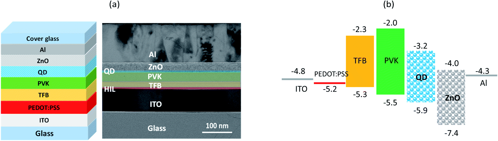 | ||
| Fig. 1 (a) Configuration and cross-sectional TEM image for the TFB/PVK device and (b) energy diagram of the QDLED. | ||
 | ||
| Fig. 2 (a) B–J–V curves, (b) CE–EQE–J curves, and (c) EL spectra of TFB device, PVK device and TFB/PVK devices with various PVK thickness. The inset of (c) depicts the EL spectra between 400 and 430 nm. | ||
| Device | Va (V) | CEb (cd A−1) | EQEc (%) | Wavelength (nm) | FWHM (nm) | LT50 (min) |
|---|---|---|---|---|---|---|
| a Measured at J = 1 mA cm−2.b Maximum CE.c Maximum EQE. | ||||||
| TFB | 2.7 | 0.38 | 0.6 | 466.1 | 21.9 | 44 |
| TFB/PVK (7 nm) | 3.5 | 0.75 | 1.2 | 465.5 | 22.9 | — |
| TFB/PVK (14 nm) | 3.6 | 2.53 | 4.1 | 464.8 | 21.3 | — |
| TFB/PVK (28 nm) | 5.4 | 3.41 | 5.6 | 464.8 | 20.3 | 76 |
| PVK | 5.3 | 1.74 | 2.9 | 470.0 | 25.9 | — |
For the operational lifetimes, TFB and TFB/PVK (28 nm) devices were chosen to stress with an initial luminance of 500 cd m−2. Fig. 3 depicts the luminescence decay curves and voltage increase curves over time. The luminance decreased to 30% of the initial luminance. LT50 of the TFB/PVK device significantly increased to 76 min, which corresponds to an improvement by a factor of 1.72, whereas that of the TFB device was only 44 min (LTX indicates the time at which luminance decreases to X% of the initial luminance). The PVK device exhibited a higher voltage increase than did the TFB/PVK device. The voltage increase over time occurred due to material degradation, which led to the formation of trap sites that could capture the carrier. This finding indicates that the TFB device suffered significantly more material damage than did the TFB/PVK device and the TFB/PVK structure can inhibit material degradation. To deeply understand the underlying mechanisms of performance enhancement and the elongation of the operational lifetime, TREL and steady-state PL were examined.
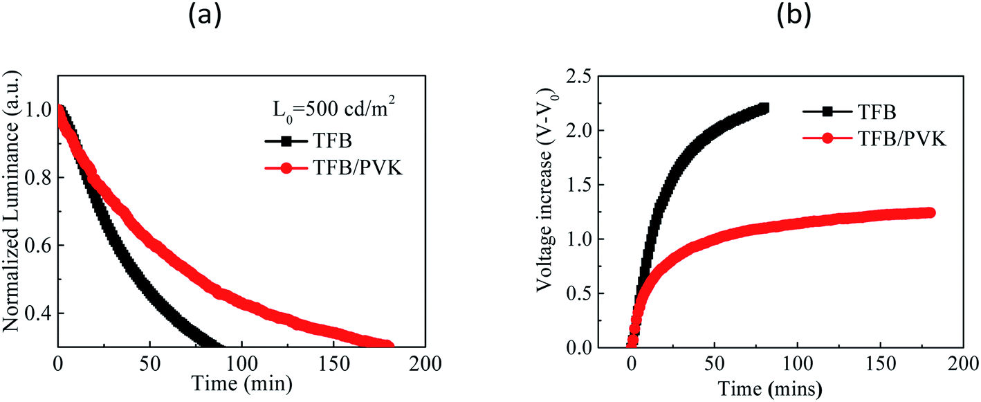 | ||
| Fig. 3 (a) Luminance decay curves over time and (b) voltage increase (V–V0) curves over time for the TFB and TFB/PVK (28 nm) devices. | ||
Analysis of device dynamics
TREL data are used to investigate the carrier and exciton dynamics between fresh and aged devices. For example, the carrier injection and transportation behaviors can be observed by tracing a TREL signal at the turn-on and rise of a square pulse.39–41 In TREL, a delayed time (Td) can be detected at starting point between voltage driving (time zero) and optical signals, which is typically attributable to the timespan of carrier injection and transport to the emission zone as represented by eqn (S1).† The residual and trapped carriers in the device and the long-lived exciton decay behavior can be observed by tracing the TREL signal at the turn-off and falling of the square pulse. Fig. 4a and b present TREL results at the rise of a square pulse for TFB and TFB/PVK devices, respectively. Td for the fresh TFB and TFB/PVK devices were determined to be 1.93 and 2.68 μs, respectively. The Td difference between them was 0.75 μs was resulted from the hole transporting mobility relied on PVK. In addition, this Td could be utilized to calculate the carrier mobility (see ESI†), the hole transporting mobility of approximately 7.46 × 10⁻⁶ cm2 S−1 V−1 for PVK was obtained, which totally agreed with the previous report.37 After aging, the delay time increased for both devices, and a larger increase in delay time was observed for the TFB device than for the TFB/PVK device. Typically, an increase in the delay time indicates poor carrier transport, which is attributable to material degradation, which can lead to the formation of carrier-trapping sites. Therefore, the TFB device suffered more material degradation than did the TFB/PVK device. In addition, both devices exhibited different EL rising behaviors. EL rose quickly and gradually reached a steady-state for TFB and TFB/PVK devices, respectively. Therefore, the rising time of the TFB device was shorter than that of the TFB/PVK device, which is attributed to the different hole-transporting behaviors of the two devices. Hole transport in TFB is nondispersive, whereas that in PVK is dispersive.42–44 For the TFB/PVK device, holes were transported dispersively in the PVK layer and injected into the EML; thus, the EL of this device increased gradually. | ||
| Fig. 4 TREL measured at 5 V, which represents the rise of the square pulse, for the (a) TFB and (b) TFB/PVK (28 nm) device as well as the decay time of the TREL measured at J = 10 mA cm−2, which represents the fall of the square pulse, for the (c) TFB and (d) TFB/PVK devices. | ||
Fig. 4c and d present the decay curves for the TFB and TFB/PVK devices, respectively. The decay times for the fresh TFB and TFB/PVK devices are 4.08 and 3.71 μs, respectively. The decay times (on the order of microseconds) of these devices were longer than the intrinsic decay time (on the order of nanoseconds) of the QD thin film; thus, another origin for the long EL decay might exist, such as the recombination of residual or trapped carriers in the device that becomes detrapped and then recombines to generate delayed EL after the end of the square pulse. The TFB/PVK device exhibited a shorter decay time than did the TFB device; thus, compared to the TFB device, the TFB/PVK device had fewer residual carriers and more carrier balance, which might be the origin of the higher efficiency of the TFB/PVK device. After aging, the decay time of the TFB device increased to 5.46 μs. This long decay time and the appearance of a large spike suggested that excess residual carriers or trapped carriers exist in the device after aging.45 The aforementioned increase in the decay time implies that an increased number of carriers were trapped during aging and acted as quenchers of the excitons, which led to luminance loss and decreased efficiency.46 The aged TFB/PVK device exhibited a decay time of 4.00 μs, which is similar to that observed for the fresh device (3.71 μs), and a relatively small spike (Fig. 4d). These results indicate the occurrence of less material degradation in the TFB/PVK device after aging. In general, the aforementioned-trapped sites and carriers arose due to material degradation.
To verify the material degradation, the steady-state PL of the devices was analyzed. First, a xenon lamp with a wavelength of 280 nm was used to excite the device, then, the PL emission of each layer in the device, including HTL, ETL, and QD layers, was observed. The experimental setup is presented in Fig. 5a. The PL of fresh and aged devices was compared to identify material stability achieved on aging. Fig. 5b and c present the PL spectra for TFB and TFB/PVK devices, respectively, at EL intensities of 100% (fresh) and 30% (aged). To evaluate the amount of material degradation, the PL difference was obtained by subtracting the aged PL spectrum from the initial PL spectrum, as displayed in Fig. 5d. In addition, several crests are observed in the PL spectrum (Fig. 5b). The QDs exhibited an emissive peak wavelength of approximately 465 nm, and the emission of the carrier transport layers, which corresponds to the emission from ZnO and TFB, occurred within the wavelength range of 350–425 nm. However, Fig. 5c indicates that the emissive peak of TFB at approximately 418 nm vanishes and becomes unidentifiable, which is attributed to an emission of PVK accounting for the total PL spectra (Fig. S2†). The PL intensity of QDs decreased after aging. The reduction in the QD intensity for TFB and TFB/PVK devices was 35% and 11%, respectively, which corresponded to decreases of approximately 550 and 200 in the counts of the PL intensity, respectively (Fig. 5d). The TFB/PVK device exhibited a marginally different PL spectrum to that of the TFB device. The TFB/PVK device exhibited less QD degradation than did the TFB device, which is attributable to the carrier balance created in the TFB/PVK device. This result indicates that the elongation of the operational lifetime is attributable to a decrease in material degradation. However, the PL intensity loss of QDs was less than their EL intensity loss after aging. Therefore, other reasons account for the degradation. As indicated in Fig. 5b and d, the PL of the TFB device (418 nm) decreased and the TFB layer experienced serious degradation. However, the PLs of the TFB layer for the aged and fresh TFB/PVK devices were almost the same and indicated that HTL of the TFB/PVK device marginally degraded, as displayed in Fig. 5c and d. Consequently, the elongation of the operational lifetime is attributable to the decreased degradation of HTL and QDs. The decreased degradation of HTL (TFB or PVK) can be ascribed to the following reasons: (i) PVK sufficiently confines the electrons to prevent them from damaging the TFB layer28 and (ii) PVK exhibits more robust material stability against electrons than TFB does.
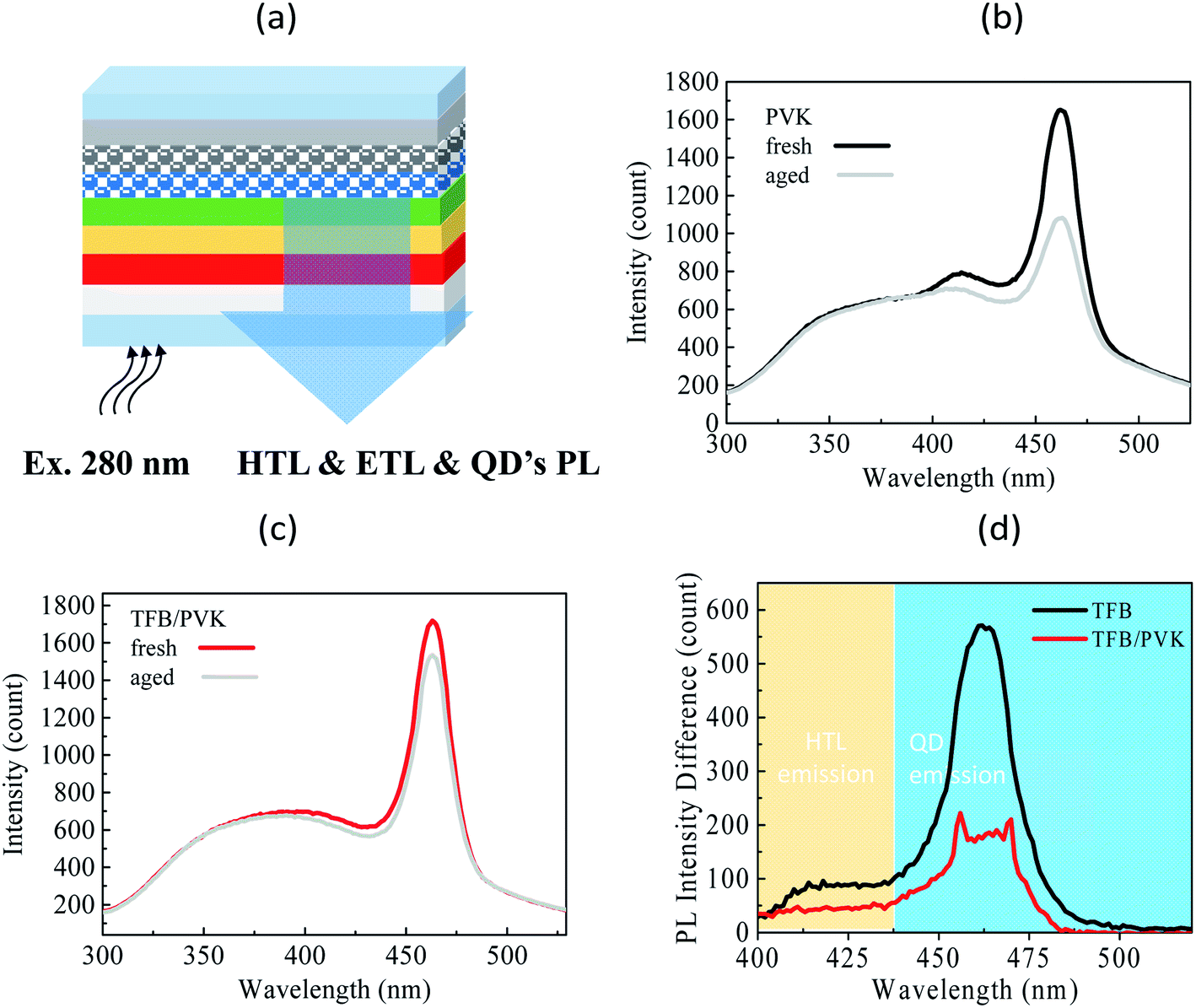 | ||
| Fig. 5 (a) Schematic of the steady-state PL spectrum; (b) PL spectra for the TFB device, where the black and gray lines denote the spectra for the fresh and aged devices, respectively; (c) PL spectra for the TFB and TFB/PVK devices, where the red and gray lines denote the spectra for the fresh and aged devices, respectively; and (d) PL difference between the TFB and TFB/PVK devices. | ||
To validate the electron-confinement ability and material stability of TFB and PVK, an EOD with the following structure was fabricated: ITO/ZnO/HTL/ZnO/Al, which refers to an EOD with structure: ITO/ZnO/QDs/ZnO/Al, used in the literature29 and modified from that. Here, the QD layer was replaced with HTL and TFB or PVK was used to observe the electron current flows for a comparison of electron-confinement ability. The fabrication parameters of EOD are identical to that of the device. The J–V curves of EOD are presented in Fig. 6a. The driving voltages of the TFB-EOD and PVK-EOD at J = 1 mA cm−2 were 0.3 and 0.7 V, respectively. The driving voltage of the PVK-EOD was higher than that of the TFB-EOD at a constant current density, which implies that PVK has superior electron-confinement ability of TFB. Both EODs were stressed at J = 25 mA cm−2 when observing the voltage variation over time during the test of material stability against electrons, as displayed in Fig. 6b. In addition, no voltage increase was observed for the PVK-EOD. However, an evident voltage increase was observed for the TFB-EOD, which indicates that TFB exhibits poor material stability against electrons. The aforementioned results validate our inference.
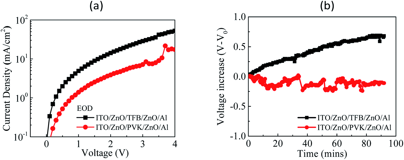 | ||
| Fig. 6 (a) J–V curves of the TFB-EOD and PVK-EOD and (b) V–V0 curves over time for the TFB-EOD and PVK-EOD measured at J = 25 mA cm−2. | ||
The aforementioned results clearly indicate the carrier dynamics and the degradation mechanism of TFB and TFB/PVK devices. The electron carriers and hole carriers are imbalanced in the TFB device. Moreover, the electrons migrate to the TFB layer, which results in leakage emission and induces material degradation as well. The EML is rich in hole carriers due to the leakage of electrons, and the excess holes cause Auger recombination, which leads to decreased efficiency and QD degradation. By contrast, in the TFB/PVK device, the PVK layer with a shallow LUMO level confines the electrons inside the QD layer for generating carrier balance and prevents electrons from leaking to the TFB layer. Due to these two advantages, high device efficiency and a long operational lifetime are achieved.
Conclusions
The device performances of QDLED were greatly improved by inserting a PVK layer at the interface of TFB HTL and QD EML. The PVK layer plays a crucial role in increasing a 9-fold efficiency and a 1.72-fold operational lifetime. These results were due to the improved hole injection, electron confinement and carrier balance in the QD EML, as well as the inhibition of HTL degradation. The carrier balance inside EML alleviated QD degradation and benefited the device efficiency and lifetime. In addition, PVK exhibits the electron-stability behavior to inhibit the electron-induced degradation on HTL, which contributes to the elongated lifetime.Conflicts of interest
There are no conflicts to declare.Acknowledgements
This work was supported by the Ministry of Science and Technology (MOST), Taiwan, under Grants MOST 109-2622-E-155-014, 108-2221-E-155-051-MY3, 108-2912-I-155-504, 108-2811-E-155-504, 107-2221-E-155-058-MY3, 107-2221-E-002-156-MY3, 107-2221-E-155-027, 107-3113-E-155-001-CC2, 106-3113-E-155-001-CC2, 106-2221-E-155-036, 106-2923-E-155-002-MY3, 106-2923-E-002-004-MY3, 105-2221-E-002-130-MY3, the MEGA project, which has received funding from the European Union's Horizon 2020 Research and Innovation Programme under the Marie Skłodowska-Curie grant agreement no. 823720 and Academia Industry Collaboration Project under number of 1909059, which was funding by AU Optronics Corporation, Taiwan.References
- S. Oh and J. Kim, Appl. Sci., 2019, 9(21), 4539 CrossRef CAS.
- W. C. Ding, C. Y. Lee, C. H. Chen, L. J. Huang, Y. P. Kuo, P. Y. Chen, H. H. Lu and J. H. Lee, SID Int. Symp. Dig. Tech. Pap., 2019, 50(1), 1700–1701 CrossRef CAS.
- L. Gao, L. N. Quan, F. P. G. de Arquer, Y. Zhao, R. Munir, A. Proppe, R. Quintero-Bermudez, C. Zou, Z. Yang, M. I. Saidaminov, O. Voznyy, S. Kinge, Z. H. Lu, S. O. Kelly, A. Amassian, J. Tang and E. H. Sargent, Nat. Photonics, 2020, 14(4), 227–233 CrossRef CAS.
- X. Li, Y. B. Zhao, F. Fan, L. Levina, M. Liu, R. Quintero-Bermudez, X. Gong, L. N. Quan, J. Z. Fan, Z. Yang, S. Hoogland, O. Voznyy, Z. H. Lu and E. H. Sargent, Nat. Photonics, 2018, 12, 159–164 CrossRef CAS.
- S. Oh, C. Y. Han, H. Yang and J. Kim, Nanoscale, 2019, 11(19), 9276–9280 RSC.
- S. K. Kim and Y. S. Kim, J. Appl. Phys., 2019, 126(3), 035704 CrossRef.
- D. Y. Park, J. H. Lim, M. Y. Ha and D. G. Moon, J. Nanosci. Nanotechnol., 2020, 20(7), 4454–4457 CrossRef CAS PubMed.
- S. Kumar, J. Jagielski, T. Tian, N. Kallikounis, W. C. Lee and C. J. Shih, ACS Energy Lett., 2018, 4(1), 118–125 CrossRef.
- S. Kumar and C. J. Shih, J. Appl. Phys., 2020, 128(12), 120901 CrossRef CAS.
- I. P. Liu, L. Y. Chen and Y. L. Lee, J. Power Sources, 2016, 325, 706–713 CrossRef CAS.
- J. Kwak, J. Lim, M. Park, S. Lee, K. Char and C. Lee, Nano Lett., 2015, 15(6), 3793–3799 CrossRef CAS PubMed.
- N. J. L. K. Davis, J. R. Allardice, J. Xiao, A. Karani, T. C. Jellicoe, A. Rao and N. C. Greenham, Mater. Horiz., 2019, 6, 137–143 RSC.
- G. J. Supran, K. W. Song, G. W. Hwang, R. E. Correa, J. Scherer, E. A. Dauler, Y. Shirasaki, M. G. Bawendi and V. Bulović, Adv. Mater., 2015, 27(8), 1437–1442 CrossRef CAS PubMed.
- X. Wang, G. I. Koleilat, J. Tang, H. Liu, I. J. Kramer, R. Debnath, L. Brzozowski, D. A. R. Barkhouse, L. Levina, S. Hoogland and E. H. Sargent, Nat. Photonics, 2011, 5, 480–484 CrossRef CAS.
- J. Bao and M. G. Bawendi, Nature, 2015, 523(7558), 67–70 CrossRef CAS PubMed.
- H. Shen, Q. Gao, Y. Zhang, Y. Lin, Q. Lin, Z. Li, L. Chen, Z. Zeng, X. Li, Y. Jia, S. Wang, Z. Du, L. S. Li and Z. Zhang, Nat. Photonics, 2019, 13, 192–197 CrossRef CAS.
- V. L. Colvin, M. C. Schlamp and A. P. Alivisatos, Nature, 1994, 370, 354–357 CrossRef CAS.
- H. Peng, W. Wang and S. Chen, IEEE Electron Device Lett., 2015, 36(4), 369–371 CAS.
- W. Ji, Y. Tian, Q. Zeng, S. Qu, L. Zhang, P. Jing, J. Wang and J. Zhao, ACS Appl. Mater. Interfaces, 2014, 6(16), 14001–14007 CrossRef CAS PubMed.
- S. Pradhan, F. Di Stasio, Y. Bi, S. Gupta, S. Christodoulou, A. Stavrinadis and G. Konstantatos, Nat. Nanotechnol., 2019, 14(1), 72–79 CrossRef CAS PubMed.
- W. Zhang, Z. Wu, X. Zhang, S. Liang, B. Jiao and X. Hou, Chin. Sci. Bull., 2011, 56(21), 2210–2214 CrossRef CAS.
- Q. Su, H. Zhang, Y. Sun, X. W. Sun and S. Chen, ACS Appl. Mater. Interfaces, 2018, 10, 23218–23224 CrossRef CAS PubMed.
- Q. Chen, Y. Yan, X. Wu, X. Wang, G. Zhang, J. Chen, H. Chen and T. Guo, J. Mater. Chem. C, 2020, 8, 1280–1285 RSC.
- L. Wang, Y. Lv, J. Lin, Y. Fan, J. Zhao, Y. Wang and X. Liu, Nanoscale, 2017, 9(20), 6748–6754 RSC.
- K. P. Acharya, A. Titov, J. Hyvonen, C. Wang, J. Tokarz and P. H. Holloway, Nanoscale, 2017, 9, 14451–14457 RSC.
- Q. Su, Y. Sun, H. Zhang and S. Chen, Adv. Sci., 2018, 5, 1800549 CrossRef PubMed.
- Y. Liu, C. Jiang, C. Song, J. Wang, L. Mu, Z. He, Z. Zhong, Y. Cun, C. Mai, J. Wang and Y. Cao, ACS Nano, 2018, 12(2), 1564–1570 CrossRef CAS PubMed.
- X. Xue, J. Y. Dong, S. Wang, H. Z. Zhang, H. Zhang, J. Zhao and W. Ji, J. Mater. Chem. C, 2020, 8, 2014–2018 RSC.
- S. Chen, W. Cao, T. Liu, S. W. Tsang, Y. Yang, X. Yan and L. Qian, Nat. Commun., 2019, 10(1), 1–9 CrossRef PubMed.
- T. Davidson-Hall and H. Aziz, Nanoscale, 2018, 10(5), 2623–2631 RSC.
- T. Davidson-Hall and H. Aziz, Nanoscale, 2019, 11(17), 8310–8318 RSC.
- D. Zou, M. Yahiro and T. Tsutsui, Appl. Phys. Lett., 1998, 72(19), 2484–2486 CrossRef CAS.
- Y. Yang, A. Titov, J. Hyvonen, Y. Zheng, L. Qian and P. H. Holloway, US Pat., 9780256B2, 2017 Search PubMed.
- Y. Sun, Y. Jiang, X. W. Sun, S. Zhang and S. Chen, Chem. Rec., 2019, 19(8), 1729–1752 CrossRef CAS PubMed.
- H. Zhang, S. Chen and X. W. Sun, ACS Nano, 2018, 12(1), 697–704 CrossRef CAS PubMed.
- N. J. Davis, J. R. Allardice, J. Xiao, A. Karani, T. C. Jellicoe, A. Rao and N. C. Greenham, Mater. Horiz., 2019, 6(1), 137–143 RSC.
- J. Pan, J. Chen, Q. Huang, L. Wang and W. Lei, RSC Adv., 2017, 7(69), 43366–43372 RSC.
- J. H. Lee, B. Y. Lin, Y. H. Lan, T. L. Chiu, P. Y. Lee and C. F. Lin, Org. Electron., 2015, 24, 182–187 CrossRef CAS.
- W. Brütting, H. Riel, T. Berierlein and W. Riess, J. Appl. Phys., 2001, 89, 1704 CrossRef.
- M. Ichikawa, J. Amagai, Y. Horiba, T. Koyama and Y. Taniguchi, J. Appl. Phys., 2003, 94, 7796 CrossRef CAS.
- B. Wei, K. Furukawa, J. Amagai, M. Ichikawa, T. Koyama and Y. Tanguchi, Semicond. Sci. Technol., 2004, 19, L56–L59 CrossRef CAS.
- H. H. Fong, A. Papadimitratos and G. G. Malliaras, Appl. Phys. Lett., 2006, 89, 172116 CrossRef.
- A. P. Tyutnev, V. S. Saeko, E. D. Pozhidaev and V. A. Kolesnikov, J. Phys.: Condens. Matter, 2006, 18, 6365 CrossRef CAS.
- F. C. Bos, T. Guion and D. M. Burland, Phys. Rev. B: Condens. Matter Mater. Phys., 1889, 39, 12633 CrossRef PubMed.
- D. Kasemann, R. Brückner, H. Fröb and K. Leo, Phys. Rev. B: Condens. Matter Mater. Phys., 2011, 84(11), 115208 CrossRef.
- T. Y. Cheng, J. H. Lee, C. H. Chen, P. H. Chen, P. S. Wang, C. E. Lin, B. Y. Lin, Y. H. Lan, Y. H. Hsieh, J. J. Huang, H. F. Lu, I. Chao, M. k. Leung, T. L. Chiu and C. F. Lin, Sci. Rep., 2019, 9, 365 CrossRef PubMed.
Footnote |
| † Electronic supplementary information (ESI) available. See DOI: 10.1039/d1ra03310g |
| This journal is © The Royal Society of Chemistry 2021 |