
 Open Access Article
 This Open Access Article is licensed under a Creative Commons Attribution-Non Commercial 3.0 Unported Licence
Enhanced dielectric properties with a significantly reduced loss tangent in (Mg2+, Al3+) co-doped CaCu3Ti4O12 ceramics: DFT and experimental investigations†
Jakkree Boonlakhorn ab,
Jedsada Manyamc,
Sriprajak Krongsukab,
Prasit Thongbaiab and
Pornjuk Srepusharawoot*ab
ab,
Jedsada Manyamc,
Sriprajak Krongsukab,
Prasit Thongbaiab and
Pornjuk Srepusharawoot*ab
aGiant Dielectric and Computational Design Research Group (GD-CDR), Department of Physics, Faculty of Science, Khon Kaen University, Khon Kaen 40002, Thailand. E-mail: spornj@kku.ac.th
bInstitute of Nanomaterials Research and Innovation for Energy (IN-RIE), NANOTEC-KKU RNN on Nanomaterials Research and Innovation for Energy, Khon Kaen University, Khon Kaen 40002, Thailand
cNational Nanotechnology Center (NANOTEC), National Science and Technology Development Agency (NSTDA), Pathum Thani 12120, Thailand
First published on 19th July 2021
Abstract
CaCu3Ti4O12 and CaCu2.95Mg0.05Ti3.95Al0.05O12 ceramics were fabricated via a solid-state reaction method. A single-phase of CaCu3Ti4O12 was found in these two ceramics. Very great grain size expansion was produced by co-doping with Mg2+ and Al3+. DFT results indicate that both Mg and Al atoms preferentially occupy Cu sites, creating liquid-phase sintering decomposition at grain boundary layers. Very high dielectric permittivity of ∼58![[thin space (1/6-em)]](https://www.rsc.org/images/entities/char_2009.gif) 397 and low loss tangent of about 0.047 were achieved in a CaCu2.95Mg0.05Ti3.95Al0.05O12 ceramic. Additionally, the temperature stability of the dielectric response was improved. Better dielectric properties in the co-doped ceramic have possible origins from enhanced grain boundary responses, especially from the influences of metastable phases and oxygen enrichment at the grain boundaries. Experimental and computational results indicate that the colossal dielectric properties in CaCu3Ti4O12 ceramics might be correlated with an internal barrier layer capacitor structure.
397 and low loss tangent of about 0.047 were achieved in a CaCu2.95Mg0.05Ti3.95Al0.05O12 ceramic. Additionally, the temperature stability of the dielectric response was improved. Better dielectric properties in the co-doped ceramic have possible origins from enhanced grain boundary responses, especially from the influences of metastable phases and oxygen enrichment at the grain boundaries. Experimental and computational results indicate that the colossal dielectric properties in CaCu3Ti4O12 ceramics might be correlated with an internal barrier layer capacitor structure.
Introduction
Nowadays, simple and complex oxides with their unique physical properties can be converted to essential electronic manufacturing elements to produce a variety of electronic devices.1–19 The development of complex perovskites for use in materials for energy storage applications has been extensively reported over the past ten years.1–12,20 One of the many improvements of ceramic dielectrics and related materials is used as the capacitive components of capacitors. However, almost all ceramic capacitors are produced using ferroelectric materials such as PbTiO3.1 Up to the present time, many types of advanced ceramics, ceramic–polymer composites, metal–polymer composites, and other related materials, have been candidates for capacitive materials. Considering capacitors and other electronic applications, the dielectric and electrical properties of co-doped TiO2,13–17 co-doped SnO2,18,19 and single- as well as co-doped CaCu3Ti4O12 (CCTO)2–6 have been investigated and reported. Simultaneously, ceramic–polymer and metal–ceramic–polymer composite materials have also been suggested to be new high-performance dielectric materials with outstanding physical properties, such as being flexible and environmentally friendly, among others.21–24 The CCTO ceramic has impressive dielectric properties in terms of its high-dielectric permittivity (ε′ ∼103 to 105) at 1 kHz and room temperature (RT).2–8 The origin of the giant dielectric properties of CCTO is still unclear. An internal barrier layer capacitor (IBLC) model has been widely accepted as the primary origin of the giant dielectric response.2–8 Insulating grain boundaries (GB) and semiconducting grains in the CCTO structure are closely related to this dielectric model.25 In addition to the microscopic scale based on an IBLC, the nanoscale barrier layer capacitance (NBLC) mechanism and the influence of domain boundaries, attributed to the potential barriers formed by the intrinsic structural defects, have also been accepted to be the nanoscopic origins of its giant dielectric response.26,27 In specific cases, sample–electrode contact,9 intrinsic defects due to charge compensation,28 and other defect clusters29,30 are much more dominant than the IBLC, NBLC, and domain boundary effects. Therefore, the IBLC model and other possible origins should be considered to accurately describe the giant dielectric behaviour of CCTO ceramics.There are many ways to improve the dielectric properties of CCTO ceramics by significantly reducing their loss tangent (tanδ).2–8 This is effective since a relatively high tanδ is the most severe barrier of this perovskite oxide to practical use in capacitor applications. Preparation and sintering methods have been modified to prepare low energy loss materials.2,3,7,8 Also, the substitution of metal ions into the lattice has been examined to produce highly capacitive ceramics with low loss factors.3–6 According to earlier works with co-doped TiO2 and co-doped SnO2, co-substitutions of (Nb5+, In3+),14 (Nb5+, Al3+),13,19 (Nb5+, Cr3+),18 (Nb5+, Zn2+),15 (Ta5+, Al3+),16 and (Nb5+, Gd3+),17 among others, can enhance ε′ values while reducing tanδ. Additionally, enhancement of dielectric properties with reduced tanδ values can be done via co-substitution of (Ni2+, Ge4+),10,11 (Sr2+, Ge4+),12 (Zn2+, Zr4+),5 and (Zn2+, Al3+)4 in a CCTO lattice. Interestingly, experimental results indicate that co-doping of metal ions in the CCTO structure can improve its giant dielectric response. Interestingly, previous research studies have investigated the construction and design of defects generated in the lattice of oxides to study the impact of intrinsic defects on the physical properties of each work.11,12,31–33 Also, earlier works with (Ni2+, Ge4+)11 and (Sr2+, Ge4+)12 dopants in CCTO ceramics investigated the dielectric and electrical responses as well as their origins by employing experimental and computational methods. It was found that one of two dopants could occupy some sites in unexpected ways (e.g., Ge4+ preferentially occupies Cu2+ sites rather than Ti4+), causing a decomposition of metastable insulating phases at GBs. Additionally, the computational results indicate that an influence of co-substitution is a decrease in oxygen loss. As a result, the total energy loss factor can be reduced in these two ways. Although investigations of co-doped CCTO ceramics have been extensively reported, only experimental factors have been presented. It is reasonable to propose that experimental work combined with computational methods based on advanced dielectric and electrical properties may provide great insights. Using the co-doping concept of our previous work, we changed dopants as Ni2+ → Mg2+ and Ge4+ → Al3+ since these conditions have not yet been reported. Thus, these preparations and characterizations were systematically made.
In this research, a solid-state reaction (SSR) method was chosen to synthesize the CaCu3Ti4O12 and CaCu2.95Mg0.05Ti3.95Al0.05O12 ceramics. Structural, dielectric, and electrical factors were systematically examined. Also, the stable structure of Mg and Al codoped CCTO structure was inspected through density functional theory (DFT). The stable location of oxygen vacancies in (Mg2+, Al3+) doped CCTO lattice was scrutinized. Details of fabrication, characterization, results, and a discussion are presented in the following.
Experimental details
1. Ceramic preparation
MgO (Sigma-Aldrich, 99.99% purity), Al2O3 (Sigma-Aldrich, 99.99% purity), TiO2 (Sigma-Aldrich, 99.9% purity), CuO (Sigma-Aldrich, 99.0% purity), CaCO3 (Sigma-Aldrich, 99.0% purity), and C2H5OH (RCI Labscan, 99.5% purity) were used in the preparation of CaCu3Ti4O12 and CaCu2.95Mg0.05Ti3.95Al0.05O12 ceramics via a SSR method. First, stoichiometric quantities of starting raw metallic materials for these two conditions were mixed with C2H5OH and zirconia balls in plastic bottles. Then, the bottles were used as ball mills rotating at 200 rpm for 24 h. Second, the mixed raw materials were dried in an oven at 80 °C for ∼24 h. Third, the resulting powders were calcined at 850 °C for 12 h. Details of forming pellet-shaped bodies have been previously published.34 The pellet bodies were sintered in air at 1050 °C for 3 h. In this work, the sintered CaCu3Ti4O12 and CaCu2.95Mg0.05Ti3.95Al0.05O12 ceramics are references as the CCTO and Mg05Al05 samples, respectively.2. Characterizations
Crystal structure and phase arrangements of the sintered samples were characterized using X-ray diffractometry (XRD, PANalytical, EMPYREAN) coupled with HighScore Plus Software Version 3.0e. The XRD patterns were collected over the 2θ range of 20°–80° using a step increase of 0.01°. The XRD data were analyzed using the Rietveld refinement method. The refinement factors are given in previous work.34 A desktop scanning electron microscope (MiniSEM, SNE-4500M) was performed to investigate a morphology of our fabricated ceramics. An energy-dispersive X-ray spectroscopy (EDS) technique was used to research the dispersion of various common elements. Valence states of the Cu and Ti were determined using X-ray photoelectron spectroscopy (XPS, AXIS Ultra DLD).3. Computational calculations
DFT calculations were done using the Vienna Ab initio Simulation Package (VASP)35 to determine the lowest-energy configuration of the Mg and Al dopants in the CCTO structure. Moreover, the most stable position of oxygen vacancy (VO) in the Mg and Al codoped CCTO lattice was also considered. Computational details are given in our previous work.12 With the Projector Augmented Waves (PAW) pseudopotential used in the present work, we chose 2p and 3s valence states for Mg and 3s and 3p valence states for Al.4. Dielectric and electrical tests
Sample surfaces were polished to prepare smooth surface layers before applying an Au film coating. A Polaron SC500 sputter coating unit was used in the Au deposition process for dielectric and electrical tests. Dielectric and electrical measurements were carried over respective temperature and frequency ranges of −60 to 210 °C and 40 to 107 Hz using an impedance analyzer (KEYSIGHT E4990A) coupled with a temperature controller (Delta Design Chamber 9023 model). The oscillation voltage (Vrms) for dielectric measurements was 500 mV.Results and discussion
XRD patterns of the CCTO and Mg05Al05 samples are shown in Fig. 1(a). A single CCTO phase (JCPDS No. 75-2188) was found in these two ceramics. XRD spectra specify a body-centered cubic (bcc) structure with an Im3 space group.36 No possible impurities, such as TiO2, CuO, CaTiO3, Al2O3, MgO, and other related phases, were detected. The Rietveld method was performed to analyse XRD data. Structural factors are summarized in Table 1. The R-factors, including the weighted profile R-factor (Rwt), the expected R-factor (Rexp), and the profile R-factor (Rp), were less than 6%. As a result of these small R-factors, the goodness of fit (GOF) factor was also relatively low (GOF ∼ 1.4–1.6). Structural factors of this magnitude are acceptable values for the Rietveld refinement.37 The lattice parameter (a) values of the CCTO and Mg05Al05 ceramics were 7.3936(0) and 7.3910(0) Å, respectively. Interestingly, the a value decreases when substituting with both Mg2+ and Al3+. As reported by Sun et al.,38 lattice parameter of CaCu3−xMgxTi4O12 ceramic with x = 0.05 is unchanged compared to CaCu3Ti4O12. Simultaneously, the same result can be seen in the work of Nautiyal et al.39 It is reasonable to suggest that influence of Mg2+ dopant does not affect to the change of lattice parameter of Mg05Al05. Interestingly, as reported by Choi and Hong,40 the lattice parameter of CaCu3Ti3.90Al0.10O12 (∼7.3906 Å) is smaller than that of CaCu3Ti4O12 (∼7.3937 Å), which is agreed with our work. Therefore, a slightly decrease in the lattice parameter of the Mg05Al05 ceramic might be originated by the Al3+ dopants. | ||
| Fig. 1 (a) XRD patterns of the CCTO and Mg05Al05 ceramics. (b and c) Rietveld profile fits of CCTO and Mg05Al05 ceramics, respectively. | ||
To consider the locations of dopants in the CCTO host, the ionic radii and coordination numbers are used. The ionic radius of Mg2+ with 4 nearest neighbours is equal to that of Cu2+, namely 0.57 Å.41 Although, the ionic radius of Ca2+ with 6 nearest neighbours (1.0 Å) is larger than that of Mg2+. Hence, Mg2+ dopant might substitute at Cu2+ site. Al3+ with 4 and 6 nearest neighbours has ionic radius of 0.39 and 0.535 Å, respectively. The ionic radius of Ti4+ with 6 nearest neighbours is 0.605 Å which is rather close to the radius of Al3+ with 6 nearest neighbours. Consequently, Al3+ might replace at either Cu2+ or Ti4+ site. This leads us to perform the DFT calculations using the VASP code to determine the most stable positions of both Mg and Al in the CCTO lattice. Our computational investigations (see Fig. 4 and 4S in the ESI†) revealed that both Mg and Al dopants are likely to be at Cu site. The presence of Mg2+ and Al3+ at Cu sites might suppress the oxygen loss during the sintering process; thus, the dielectric and electrical properties of CCTO might be improved.
The theoretical densities (ρT) calculated using XRD data of CCTO and Mg05Al05 ceramics were 5.0469 and 5.1174 g cm−3, as listed in Table 1. Surface morphologies and grain size distributions of sintered the CCTO and Mg05Al05 samples are shown in Fig. 2. A small degree of abnormal grain growth (grain size ∼ 80.78 ± 37.25 μm) was surrounded by fine grains (grain size ∼ 2.13 ± 0.38 μm) in the CCTO ceramic.
 | ||
| Fig. 2 SEM images and size distributions of (a) CCTO and (b) Mg05Al05 ceramics. | ||
Interestingly, the grains of the Mg05Al05 ceramic were primarily expanded by co-doping with Mg2+ and Al3+. The mean grain size of the Mg05Al05 ceramic was 302.64 ± 78.14 μm. The large increase in this ceramic grain size is likely associated with a liquid-phase sintering (LPS) mechanism.11,12,20 As disclosed in Fig. 3, EDS mapping of the Mg05Al05 ceramic showed that Mg and Al elements have suitable dispersions. Simultaneously, Ca and Ti at the grain area showed a homogeneous distribution, while these two elements are scarcely observed in the GB region. Interestingly, the Cu-rich phases were present in good quantities in the GB layers. This EDS mapping result is similar to those of other reports of the LPS mechanism.11,12,20
 | ||
| Fig. 3 EDS mapping of the Mg05Al05 ceramic showing the dispersions of Ca, Cu, Ti, Mg, and Al ions. | ||
As reported in previous research, the microstructure of Mg2+ doped CCTO ceramics fabricated using the SSR method and sintered at 1100 °C had no significant size difference.28 Thus, the Mg2+ dopant might not substantially impact grain size expansion at a relatively low sintering temperature of 1050 °C. According to our previous work, the replacement of dopant at unexpected sites might be a significant cause of these microstructural changes.11,12
It is well known that the LPS mechanism coming from the excess Cu in the CCTO host originates from the substitution of either Al or Mg at Cu sites. Consequently, the grain size is enlarged. Oppositely, this mechanism cannot be existed for the case of Al or Mg replaced at Ti sites. In general, the eutectic phases of MgO–TiO2, MgO–Al2O3, CaO–TiO2, and Al2O3–TiO2 cannot be created at a temperature lower than 1200 °C,42 whereas, this phase is formed at 950 °C in air for CuO–TiO2. In this work, the liquid phase may be formed at lower temperature (about 850 °C which is calcination temperature). This is due to the replacement of Al into Cu sites of the CCTO lattice leading to excess Cu content in the Mg05Al05. In the sintering step, the liquid phase existed at the contact zones between particles or grains in the microstructure. These can increase the diffusion rate of ions across the GB, resulting in an enhanced grain growth rate. As a result, the grain size was expressively enlarged. In the current work, to solve this assumption, DFT calculations were performed to address this issue.
In our first-principles studies, we initially tested the most preferable substitution site of both Al and Mg dopants in the CCTO host. In the current study, the CCTO structure is the Ca20Cu60Ti80O240 formula unit. This led us to calculate the formation energy when either Ca, Cu, and Ti sites in the CCTO lattice were replaced by Mg or Al atoms. A lower formation energy corresponds to a more stable structure.
As clearly illustrated in Fig. 4, the formation energies of Mg when Ca, Cu, and Ti atoms were replaced by Mg atoms are +2.39, −2.56, and +3.20 eV, respectively. Also, the formation energies of Al substituted at Ca, Cu, and Ti sites are +4.41, −3.25, and +1.44 eV, respectively. These results indicated that both Mg and Al are preferentially substituted at Cu sites in the CCTO host. In addition, we also performed extra calculations to calculate the formation energies when both Mg and Al dopants are in the CCTO host simultaneously. As presented by Fig. 4S in the ESI,† our calculation results revealed that Mg and Al atoms are likely to be occupied at Cu sites simultaneously. This finding is in excellent agreement with our experimental results, i.e., XRD and EDS mapping. The largely increased grain sizes observed in our experiments arise from the liquid-phase sintering mechanism. This mechanism is associated with Mg and Al occupancy at Cu sites in the CCTO lattice. Generally, a eutectic liquid of CuO–TiO2 can be created in air at 950 °C.43 Therefore, excess Cu generated by dopants can induce much more interaction between CuO–TiO2 at this temperature, causing greatly increased grain sizes in the Mg05Al05 ceramic. In the Mg05Al05 sample, Mg and Al atoms are substituted into Cu sites in the CCTO host. Next, the most stable structure of CCTO codoped by the Mg and Al dopants needs to be determined. In the current study, we considered two different structures, namely Structures A and B.
 | ||
| Fig. 4 Formation energies of Mg and Al occupied at Ca, Cu and Ti sites of the CCTO structure. | ||
In Structure A, depicted in Fig. 5, a Mg atom is near an Al atom in the CCTO structure. Additionally, the Mg atom does not interact with the Al atom in the CCTO host, which is presented as Structure B in Fig. 5. Our total energy calculations revealed that Structure B has a lower total energy than Structure A, 0.3 eV. Hence, Structure B is found to be the most stable. Therefore, Mg and Al atoms might homogeneously disperse in the Cu sites of the CCTO lattice.
 | ||
| Fig. 5 Total energies when Mg and Al atoms are in close proximity (Structure A) and Mg does not interact with Al in the CCTO lattice (Structure B). | ||
In the present work, we also evaluated the optical property related to the energy band theory such as total density of states (DOS) of CCTO and the Mg2+ and Al3+ co-doping CCTO. These results were found in Fig. 3S of the ESI.† It was found from our calculations that the DOS of both structures is almost identical. Therefore, the optical property of the CCTO and Mg05Al05 is indifferent. Usually, oxygen vacancies (VO) are found in our samples during the preparation process. To gain insight into the most preferable position of the VO in the Mg05Al05 structure, the total energies of various positions of VO in the Mg and Al doped CCTO structure were calculated. In the current work, three possible positions of VO in the Mg05Al05 structure were inspected. Structure I of Fig. 6 represents the VO and Mg atoms in close proximity. Additionally, the VO interacts with the Al atom, as illustrated in Structure II of Fig. 6. The VO is distant from both the Al and Mg atoms, as shown in Structure III in Fig. 6. Our results reveal that the structure giving the lowest total energy is Structure III. Hence, based on our calculations, the VO is preferentially isolated from both the Mg and Al dopant atoms. According to our stable form presented as Structure II in Fig. 6, electron-pin defects, e.g., diamond or triangular shapes, are not observed. Hence, the effect of grain boundaries directly relates to the colossal dielectric properties of the Mg05Al05 structure. In other words, the giant dielectric properties of the Mg05Al05 support the internal barrier layer capacitance (IBLC) model.
 | ||
| Fig. 6 Total energies of three different positions of an oxygen vacancy in the Mg and Al codoped CCTO. Structures I and II represent cases where the oxygen vacancy is close to an Mg atom, and the oxygen vacancy is close to an Al atom in the Mg05Al05 structure, respectively. Structure III indicated a case where the VO remains independent of both Al and Mg atoms in this structure. | ||
According to the computational results presented in Fig. 4 and 5, the LPS mechanism observed in the Mg05Al05 ceramic might be formed by placing Al3+ ions into Cu2+ sites. A previous report showed that the LPS mechanism and oxygen enrichment at GBs could improve the dielectric properties of CCTO ceramics by enhancing the GB response.10–12 Hence, in this work, the resistances of grains (Rg) and GBs (Rgb) should increase with a reduction in the low-frequency tanδ values. To confirm this assumption, electrical and dielectric property studies were done.
The electrical response of sintered samples was studied using an impedance spectroscopy technique. The complex impedance (Z* = Z′ − jZ′′) can be calculated using the following relationship:
 | (1) |
 | ||
| Fig. 7 Impedance complex Z* plots at 30 °C of CCTO and Mg05Al05 ceramics. Insets (1), (2) and (3) show high-frequency Z* plots, modelled IBLC structure, and equivalent circuit represented the electrical heterogeneous microstructure of semiconducting grain and insulating grain boundary, respectively. | ||
As shown in Structure III of Fig. 6, no Vo was produced at anion positions close to the Al and Mg ions. Also, Mg and Al ions occupied sites independently of other Mg/Al ions, as shown in Structure B of Fig. 5. Therefore, Rg of the Mg05Al05 ceramic can be increased in this way. Interestingly, the origins of the enhanced Rgb of this ceramic might have more than one cause. The first cause is similar to an increase in Rg as the VO concentration in the lattice decreases. Another crucial cause might be the presence of a metastable insulating layer produced by the LPS mechanism. These two factors may result in an enhanced Rgb. This result is similar to our earlier findings.10–12
The dielectric properties of CCTO and Mg05Al05 ceramics were systematically examined. Frequency dependencies of ε′ and tanδ at 30 °C are shown in Fig. 8 and its inset (1). The ε′ values of the Mg05Al05 ceramic are much larger than those of the CCTO ceramic throughout a frequency range of 40 to 104 Hz. Additionally, the ε′ value of the co-doped ceramic has much more frequency stability than that of the pure sample over this frequency range. As listed in Table 2, ε′ at 1 kHz of CCTO and Mg05Al05 ceramics were 23062 and 58397, respectively. The difference of ε′ values between these two samples is consistent with their microstructural factors.
 | ||
| Fig. 8 Frequency dependencies at 30 °C of ε′ of CCTO and Mg05Al05 ceramics. Insets (1) and (2) show the frequency dependency of tanδ and the temperature dependency of ε′ at 1 kHz, respectively. | ||
δ at 1 kHz and 30 °C, Rg at 30 °C, Rgb at 110 °C, activation energies of GBs (Egb) of the CCTO and Mg05Al05 ceramics
| Sample | ε′ | tanδ |
Rg (Ω cm) | Rgb (Ω cm) | Eg (eV) | Egb (eV) |
|---|---|---|---|---|---|---|
| CCTO | 23062 |
0.185 | 155 | 2.04 × 10³ | 0.077 | 0.599 |
| Mg05Al05 | 58397 |
0.047 | 430 | 1.33 × 10⁵ | 0.116 | 0.796 |
Interestingly, although the number of GB layers per unit volume of Mg05Al05 ceramic decreases, the total Rgb of Mg05Al05 ceramic is much larger than that of the pure CCTO ceramic. However, a substantial contribution of a sample–electrode contact was found in the CCTO sample due to its low resistance (its Z* spectra at 110 °C is given in the ESI†). In general, the influence of a sample–electrode contact has usually occurred in the low resistive materials or a specific environment that induces the material's resistance to decrease, for example, under DC bias.9
With removal of the impact of a sample–electrode contact from Rgb calculation, a complex electric modulus (M* = M′ + jM′′) can be considered. A M* plot can be calculated using the following equations:
| M* = jωC0Z* = M′ + jM′′ | (2) |
 | (3) |
| ωτgb = ωRgbCgb = 1 | (4) |
 is the maximal value of M′′, τgb = 1/ωmax is the variation of relaxation time. The Rgb at 110 °C estimated from M* plots of CCTO and Mg05Al05 ceramics were 2.04 × 10³ and 1.33 × 10⁵ Ω cm, respectively. Enhanced Rgb in Mg05Al05 ceramic results in a reduction of its low-frequency tanδ compared to that of CCTO, as shown in inset (2) of Fig. 8. The tanδ values at 1 kHz of CCTO and Mg05Al05 ceramics were 0.185 and 0.047, respectively. In addition to enhancing ε′ and reducing tanδ, co-doping with Mg2+ and Al3+ can suppress variations of ε′ at 1 kHz throughout a temperature range of −60 to 130 °C, as shown in inset (2) of Fig. 8. Compared to Ca0.95Sr0.05Cu3Ti3.95Ge0.05O12 ceramic,12 the dielectric permittivity and loss tangent of the Mg05Al05 are still acceptable for capacitor applications, namely dielectric permittivity ≥ 5000 and loss tangent ≤ 0.05 at 1000 ± 50 Hz at room temperature. Also, the temperature stability of the dielectric permittivity in the Mg05Al05 sample is higher than that in the Ca0.95Sr0.05Cu3Ti3.95Ge0.05O12 ceramic. For Mg05Al05 samples, the temperature coefficient of dielectric permittivity at 1000 ± 50 Hz (
 ) is rather stable over the temperature range of −60 to 130 °C, whereas, this coefficient is unchanged in the temperature range of −60 to 100 °C for Ca0.95Sr0.05Cu3Ti3.95Ge0.05O12. As previously mentioned, the dielectric property of the Ca0.95Sr0.05Cu3Ti3.95Ge0.05O12 ceramic (ref. 12) satisfies the X5R capacitor. Interestingly, the temperature stability of dielectric permittivity of the Mg05Al05 sample meets the standard of the X7R capacitor, which is better than X5R capacitor.
Frequency dependencies of M′ and M′′ of sintered samples are shown in Fig. 9. The trends for the change in the  position for both CCTO and Mg05Al05 ceramics were similar. As soon as the temperature increased, the
  position immediately moved to a higher frequency, showing thermal dielectric relaxation.28 Furthermore, this behaviour also specified a decrease of Rgb with a temperature increase. In the case of Rg, this electrical factor can be reduced by increasing temperature [data not shown].
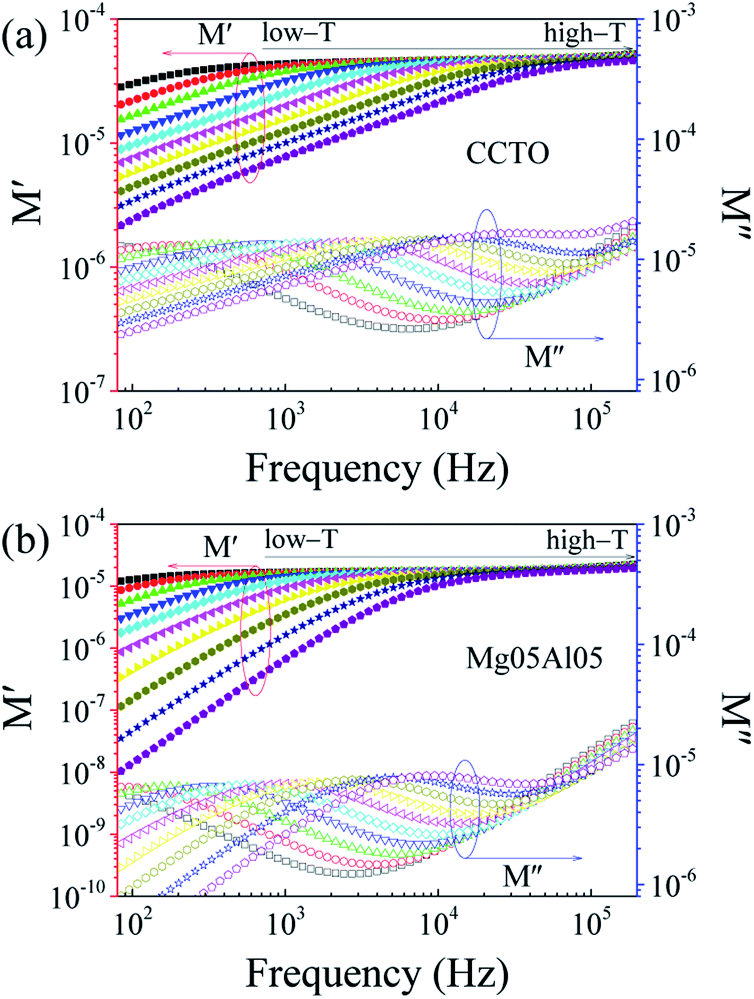 | ||
| Fig. 9 Frequency dependencies of M′ and M′′ over a wide temperature range for (a) CCTO and (b) Mg05Al05 ceramics. | ||
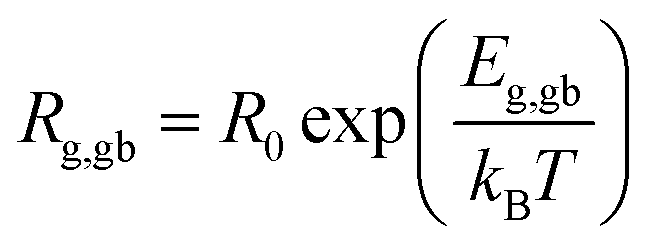
For grains (Eg) and GBs (Egb), the activation energies were evaluated by using the Arrhenius law, as follows:
 | (5) |
δ values. Oxygen enrichment and the metastable insulating layer at GBs might substantially impact the enhanced dielectric response, especially the reduced tanδ value.
 | ||
| Fig. 10 Arrhenius plots of Rg (solid symbols) and the estimated Rgb (open symbols) of CCTO and Mg05Al05 ceramics. | ||
The XPS spectra of Cu and Ti ions are illustrated in Fig. 11, showing the oxidations states of these two elements. The XPS spectra of Cu2p and Ti2p were measured in the binding energy (BE) ranges of ∼926–970 and 448–470 eV, respectively. The XPS data of transition metal ions were fitted using MultiPak software based on Gaussian–Lorentzian profile fitting. As shown in Fig. 11(a and b), the XPS Cu2p3/2 peaks of the CCTO and Mg05Al05 ceramics showed the mixing of Cu+ and Cu2+ ions. The prominent peak indicating Cu2+ was found at a BE value of ∼933.89–934.18 eV. The minor peak observed at BE ∼932.80–933.20 eV indicates the presence of Cu+. The ratios of Cu+/Cu2+ in CCTO and Mg05Al05 ceramics were ∼20.70/79.30% and ∼14.02/85.98%, respectively.
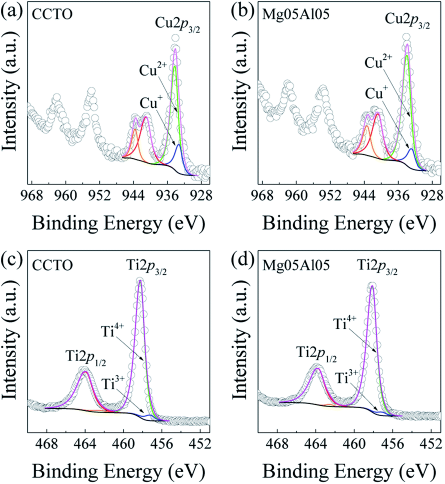 | ||
| Fig. 11 (a and b) XPS Cu2p spectra of CCTO and Mg05Al05 ceramics, respectively. (c and d) XPS Ti2p spectra of these respective ceramics. | ||
The oxidation states of Ti were also examined. Both Ti3+ and Ti4+ were found in XPS Ti2p3/2 and Ti2p1/2 peaks, as shown in Fig. 11(c and d). In the Ti2p3/2 peak, the primary peak position indicates that the Ti4+ state could be found at a BE value of ∼458.09–458.21 eV. Simultaneously, a minimal peak of Ti3+ was detected at ∼457.11–457.20 eV. The ratios of Ti3+/Ti4+ in CCTO and Mg05Al05 ceramics were ∼4.20/95.80 and ∼2.75/97.25%, respectively. The existence of Cu+ and Ti3+ signifies the existence of VO's in the ceramic lattice, inducing the structure's charge compensation mechanism to obtain a charge balance. Interestingly, percentages of Cu+ and Ti3+ are closely related to the Rg value of each sample. Besides investigating the Cu2p and Ti2p spectra, the O1s spectra were also inspected (data have been included in the ESI†). The examination shows that the O1s spectra were separated to obtain two peaks. The first peak was detected at the BE position ∼529.63–529.70 eV and the second peak can be observed at BE position ∼531.41–531.46 eV. The first oxygen peak depicts oxygen bonded in the lattice (OL), while the second oxygen peak indicates oxygen-deficient, showing the presence of unbounded oxygen molecules or VO.45 The ratios between OL/VO of the CCTO and Mg05Al05 ceramics were 59.81/40.19 and 67.51/32.49%, respectively. Interestingly, the XPS specifies that the substitutions of Mg2+ and Al3+ into the CCTO lattice could suppress oxygen loss during the sintering process at relatively high temperatures (VO decreased), which is consistent with the computational results. According to the previous work, the charge carrier hopping between Cu+ ↔ Cu2+ and Ti3+ ↔ Ti4+ induces a small conductivity inside the grains;28,46 therefore, a slight increase in Rg of the Mg05Al05 ceramic might be caused by a decrease of Cu+ and Ti3+ (VO decreases). Also, the n-type semiconductive region inside the grains might have been from charge carrier hopping between Cu+ ↔ Cu2+ and Ti3+ ↔ Ti4+. Therefore, the origin of colossal dielectric permittivity might have been derived from an IBLC effect.
Conclusions
This work deals with the dielectric, electrical, and structural properties of (Mg, Al) co-doped CaCu3Ti4O12. The XRD data of all sintered ceramics show a single phase of CaCu3Ti4O12. DFT results confirm that Mg2+ and Al3+ dopant ions occupied Cu2+ sites. These results are consistent with the very great grain size expansion due to the liquid-phase sintering mechanism. The enhancement of dielectric properties with very high dielectric permittivity of about 58397 and a low loss tangent of about 0.047 was accomplished in a CaCu2.95Mg0.05Ti3.95Al0.05O12 ceramic. Additionally, the temperature stability of the dielectric response was improved. The results of this work indicate that the colossal dielectric properties of these samples are associated with an internal barrier layer capacitor model. The XPS results show the presence of Cu+ and Ti3+, which might be one of many vital contributing factors to n-type semiconducting grains in CaCu3Ti4O12 based ceramics.
Author contributions
J. B., P. T., and P. S. designed this project. J. B. and P. S. performed experiments and computations. J. B., J. M., S. K., P. T., and P. S. analysed the computational and experimental data. J. B. and P. S. write the manuscript.Conflicts of interest
The authors declare no competing financial interests.Acknowledgements
We would like to acknowledge the Basic Research Fund of Khon Kaen University for financial funding. This project has been supported by Research and Graduate Studies, Khon Kaen University. Also, this work has been partially supported by the Research Network NANOTEC (RNN) program of the National Nanotechnology Center (NANOTEC), NSTDA, Ministry of Higher Education, Science, Research and Innovation (MHESI), and Khon Kaen University, Thailand (Grant No. P1851882).References
- Y. Yu, J. Yang, J. Wu, X. Gao, L. Bian, X. Li, X. Xin, Z. Yu, W. Chen and S. Dong, J. Eur. Ceram. Soc., 2020, 40, 3003–3010 CrossRef CAS.
- H. M. Kotb, M. M. Ahmad, S. Aldabal, A. Alshoaibi and A. Aljaafari, J. Mater. Sci.: Mater. Electron., 2019, 30, 18259–18267 CrossRef CAS.
- J. Sun, C. Xu, X. Zhao, J. Liang and R. Liao, IEEE Trans. Dielectr. Electr. Insul., 2020, 27, 1400–1408 CAS.
- C. Xu, X. Zhao, L. Ren, J. Sun, L. Yang, J. Guo and R. Liao, J. Alloys Compd., 2019, 792, 1079–1087 CrossRef CAS.
- D. Xu, X. Yue, J. Song, S. Zhong, J. Ma, L. Bao, L. Zhang and S. Du, Ceram. Int., 2019, 45, 11421–11427 CrossRef CAS.
- J. Tang, Y. Teng, Y. Chen, X. Zhao, S. Wang, W. Wang and R. Ahuja, Ceram. Int., 2021, 47, 10006–10012 CrossRef CAS.
- W. Wan, W. Tang, M. Tao, H. Cao, J. Luo, W.-x. Yuan and T. Qiu, J. Mater. Sci.: Mater. Electron., 2020, 31, 5360–5367 CrossRef CAS.
- P. Mao, J. Wang, S. Liu, L. Zhang, Y. Zhao and L. He, J. Alloys Compd., 2019, 778, 625–632 CrossRef CAS.
- K. Wu, Y. Huang, L. Hou, Z. Tang, J. Li and S. Li, J. Mater. Sci.: Mater. Electron., 2018, 29, 4488–4494 CrossRef CAS.
- J. Boonlakhorn, P. Kidkhunthod and P. Thongbai, Mater. Today Commun., 2019, 21, 100633 CrossRef CAS.
- J. Boonlakhorn, J. Prachamon, J. Manyam, P. Thongbai and P. Srepusharawoot, Ceram. Int., 2021, 47, 13415–13422 CrossRef CAS.
- J. Boonlakhorn, N. Chanlek, P. Thongbai and P. Srepusharawoot, J. Phys. Chem. C, 2020, 124, 20682–20692 CrossRef CAS.
- W. Hu, K. Lau, Y. Liu, R. L. Withers, H. Chen, L. Fu, B. Gong and W. Hutchison, Chem. Mater., 2015, 27, 4934–4942 CrossRef CAS.
- W. Hu, Y. Liu, R. L. Withers, T. J. Frankcombe, L. Norén, A. Snashall, M. Kitchin, P. Smith, B. Gong, H. Chen, J. Schiemer, F. Brink and J. Wong-Leung, Nat. Mater., 2013, 12, 821–826 CrossRef CAS PubMed.
- X. Wei, W. Jie, Z. Yang, F. Zheng, H. Zeng, Y. Liu and J. Hao, J. Mater. Chem. C, 2015, 3, 11005–11010 RSC.
- H. Peng, B. Shang, X. Wang, Z. Peng, X. Chao, P. Liang and Z. Yang, Ceram. Int., 2018, 44, 5768–5773 CrossRef CAS.
- Z. Cao, J. Zhao, J. Fan, G. Li and H. Zhang, Ceram. Int., 2021, 47, 6711–6719 CrossRef CAS.
- M. Maleki Shahraki, M. Golmohammad, M. D. Chermahini, P. Mahmoudi and H. A. Moghadam, Mater. Chem. Phys., 2020, 246, 122843 CrossRef CAS.
- Y. Song, X. Wang, X. Zhang, X. Qi, Z. Liu, L. Zhang, Y. Zhang, Y. Wang, Y. Sui and B. Song, Appl. Phys. Lett., 2016, 109, 142903 CrossRef.
- L. L. Kozlinskei, A. T. de Andrade Paes, E. C. Grzebielucka, C. P. F. Borges, A. V. C. de Andrade, E. C. F. de Souza and S. R. M. Antunes, Appl. Phys. A, 2020, 126, 447 CrossRef CAS.
- P. Kum-onsa, N. Phromviyo and P. Thongbai, RSC Adv., 2020, 10, 40442–40449 RSC.
- P. Kum-onsa, N. Phromviyo and P. Thongbai, Results Phys., 2020, 18, 103312 CrossRef.
- Y. Yu, X. Wang, X. Wang, X. Li, L. Weng and X. Zhang, J. Mater. Sci.: Mater. Electron., 2020, 31, 18336–18343 CrossRef.
- A. Sasmal, A. Patra, P. S. Devi and S. Sen, Dalton Trans., 2021, 50, 1824–1837 RSC.
- D. C. Sinclair, T. B. Adams, F. D. Morrison and A. R. West, Appl. Phys. Lett., 2002, 80, 2153 CrossRef CAS.
- M. S. Ivanov, F. Amaral, V. A. Khomchenko, J. A. Paixão and L. C. Costa, RSC Adv., 2017, 7, 40695–40704 RSC.
- S. Y. Chung, I. D. Kim and S. J. L. Kang, Nat. Mater., 2004, 3, 774–778 CrossRef CAS PubMed.
- L. Ni and X. M. Chen, Solid State Commun., 2009, 149, 379–383 CrossRef CAS.
- S. Ke, H. Huang and H. Fan, Appl. Phys. Lett., 2006, 89, 182904 CrossRef.
- J. Boonlakhorn, J. Prachamon, J. Manyam, S. Krongsuk, P. Thongbai and P. Srepusharawoot, RSC Adv., 2021, 11, 16396–16403 RSC.
- W. Jian, S.-P. Wang, H.-X. Zhang and F.-Q. Bai, Inorg. Chem. Front., 2019, 6, 2660–2666 RSC.
- B. Li and H. Metiu, J. Phys. Chem. C, 2010, 114, 12234–12244 CrossRef CAS.
- H.-Y. Su and K. Sun, J. Mater. Sci., 2015, 50, 1701–1709 CrossRef CAS.
- J. Boonlakhorn, P. Thongbai, B. Putasaeng, P. Kidkhunthod, S. Maensiri and P. Chindaprasirt, J. Am. Ceram. Soc., 2017, 100, 3478–3487 CrossRef CAS.
- G. Kresse and J. Furthmüller, Comput. Mater. Sci., 1996, 6, 15–50 CrossRef CAS.
- M. A. Subramanian, D. Li, N. Duan, B. A. Reisner and A. W. Sleight, J. Solid State Chem., 2000, 151, 323–325 CrossRef CAS.
- E. Jansen, W. Schafer and G. Will, J. Appl. Crystallogr., 1994, 27, 492–496 CrossRef CAS.
- L. Sun, R. Zhang, Z. Wang, E. Cao, Y. Zhang and L. Ju, J. Alloys Compd., 2016, 663, 345–350 CrossRef CAS.
- A. Nautiyal, C. Autret, C. Honstettre, S. De Almeida Didry, M. El Amrani, S. Roger, B. Negulescu and A. Ruyter, J. Eur. Ceram. Soc., 2016, 36, 1391–1398 CrossRef CAS.
- S. W. Choi, S. H. Hong and Y. M. Kim, J. Am. Ceram. Soc., 2007, 90, 4009–4011 CAS.
- R. D. Shannon, Acta Crystallogr., Sect. A: Cryst. Phys., Diffr., Theor. Gen. Crystallogr., 1976, 32, 751–767 CrossRef.
- G. J. Janz, C. B. Allen, N. P. Bansal, R. M. Murphy and R. P. T. Tomkins, Physical properties data compilations relevant to energy storage, 1. Molten salts: Eutectic Data, 1979 Search PubMed.
- S. Y. Lee, H. E. Kim and S. I. Yoo, J. Am. Ceram. Soc., 2014, 97, 2416–2419 CrossRef CAS.
- T. B. Adams, D. C. Sinclair and A. R. West, J. Am. Ceram. Soc., 2006, 89, 3129–3135 CrossRef CAS.
- T. Kim, G. Baek, S. Yang, J. Y. Yang, K. S. Yoon, S. G. Kim, J. Y. Lee, H. S. Im and J. P. Hong, Sci. Rep., 2018, 8, 8532 CrossRef PubMed.
- X. J. Luo, Y. T. Zhang, D. H. Xu, S. S. Chen, Y. Wang, Y. Chai, Y. S. Liu, S. L. Tang, C. P. Yang and K. Bärner, Ceram. Int., 2019, 45, 12994–13003 CrossRef CAS.
Footnote |
| † Electronic supplementary information (ESI) available. See DOI: 10.1039/d1ra02896k |
| This journal is © The Royal Society of Chemistry 2021 |