
 Open Access Article
 This Open Access Article is licensed under a Creative Commons Attribution-Non Commercial 3.0 Unported Licence
Bandgap recovery of monolayer MoS2 using defect engineering and chemical doping†
Frederick Aryeetey *a,
Sajedeh Pourianejadb,
Olubukola Ayanbajoa,
Kyle Nowlinb,
Tetyana Ignatova*b and
Shyam Aravamudhan*a
*a,
Sajedeh Pourianejadb,
Olubukola Ayanbajoa,
Kyle Nowlinb,
Tetyana Ignatova*b and
Shyam Aravamudhan*a
aDepartment of Nanoengineering, North Carolina A&T State University, 2907 East Gate City Blvd, Greensboro, NC 27401, USA. E-mail: saravamu@ncat.edu; Fax: +1-336-500-0115; Tel: +1-336-285-2810
bDepartment of Nanoscience, University of North Carolina at Greensboro, 2907 East Gate City Blvd, Greensboro, North Carolina 27401, USA. E-mail: t_ignato@uncg.edu; Fax: +1-336-500-0115; Tel: +1-336-285-2820
First published on 11th June 2021
Abstract
Two-dimensional transition metal dichalcogenide materials have created avenues for exciting physics with unique electronic and photonic applications. Among these materials, molybdenum disulfide is the most known due to extensive research in understanding its electronic and optical properties. In this paper, we report on the successful growth and modification of monolayer MoS2 (1L MoS2) by controlling carrier concentration and manipulating bandgap in order to improve the efficiency of light emission. Atomic size MoS2 vacancies were created using a Helium Ion Microscope, then the defect sites were doped with 2,3,5,6-tetrafluro7,7,8,8-tetracyanoquinodimethane (F4TCNQ). The carrier concentration in intrinsic (as-grown) and engineered 1L MoS2 was calculated using Mass Action model. The results are in a good agreement with Raman and photoluminescence spectroscopy as well as Kelvin probe force microscopy characterizations.
1 Introduction
Recent advances in materials research have focused on novel, atomically thin semiconducting materials. Starting with gapless graphene,1 a broad family of two-dimensional (2D) dichalcogenide materials have been fabricated in monolayer and few-layers form.2–4 These materials possess unique properties enabling creation of a new generation of flexible and ultrathin optoelectronic devices. Among this family, direct bandgap semiconducting monolayer molybdenum disulfide (1L MoS2) is the most popular one.5,6 There are numerous reports of successful Chemical Vapor Deposition (CVD) synthesis processes. Unfortunately, CVD grown 2D MoS2 always contains sulfur vacancies resulting in the creation of unsaturated chemical bonds at the molybdenum atoms. Sulfur vacancies represented by dangling bonds may serve as active sites for chemical adsorption of species. They will also result in quenching and broadening of MoS2 photoluminescence (PL) by bringing additional defective states that are not available in the perfect system.7–12 These vacancies influence drastically the carrier concentration and exciton generation in a sample. In a perfect system two exciton states are formed at the K and K′ point of MoS2 Brillouin zone – exciton A (around 1.8 eV) and exciton B (around 2 eV). In the presence of sulfur vacancies, interaction of exciton and free carrier gives rise to the formation of a many-body bound state, a negatively charged exciton, also referred as a trion. It is already known that the PL of monolayer MoS2 can be enhanced by reducing concentration of the excessive electrons and related shift of oscillator strength between trions and excitons.13,14 Various techniques have been employed to modulate optical properties of 1L MoS2 by controlling free carrier density, namely electrical gating, gas physisorption,13,15 and chemical doping.16–19In this study, we first investigated intrinsic doping of as-grown monolayer MoS2. We later modified monolayer MoS2 using focused helium ion irradiation, consequently introducing monosulfur and disulfur vacancies predominately. The carrier concentration in as-grown and defected samples was linked with 2D MoS2 optical response. Finally, we restored/enhanced PL of defected monolayer MoS2 via chemical p-type doping.
2 Experimental procedures
2.1 Sample preparation
High quality 2D MoS2 samples were grown at 650 °C on Si/SiO2 substrates using a home-built CVD setup with a one-inch quartz tube fitted in Lindberg furnace equipment. Fig. 1a–d shows that the morphology and shape of 2D MoS2 varies depending on the stoichiometric ratio of Molybdenum to sulfur![[thin space (1/6-em)]](https://www.rsc.org/images/entities/char_2009.gif) :hexagon shape flakes grow when the ratio is 1:1, an uneven ratio will give rise to triangles. The SEM and Raman analysis confirm that the majority of MoS2 flakes are monolayers, however, some flakes, especially hexagons, have small islands of second- and third-layer.
:hexagon shape flakes grow when the ratio is 1:1, an uneven ratio will give rise to triangles. The SEM and Raman analysis confirm that the majority of MoS2 flakes are monolayers, however, some flakes, especially hexagons, have small islands of second- and third-layer.
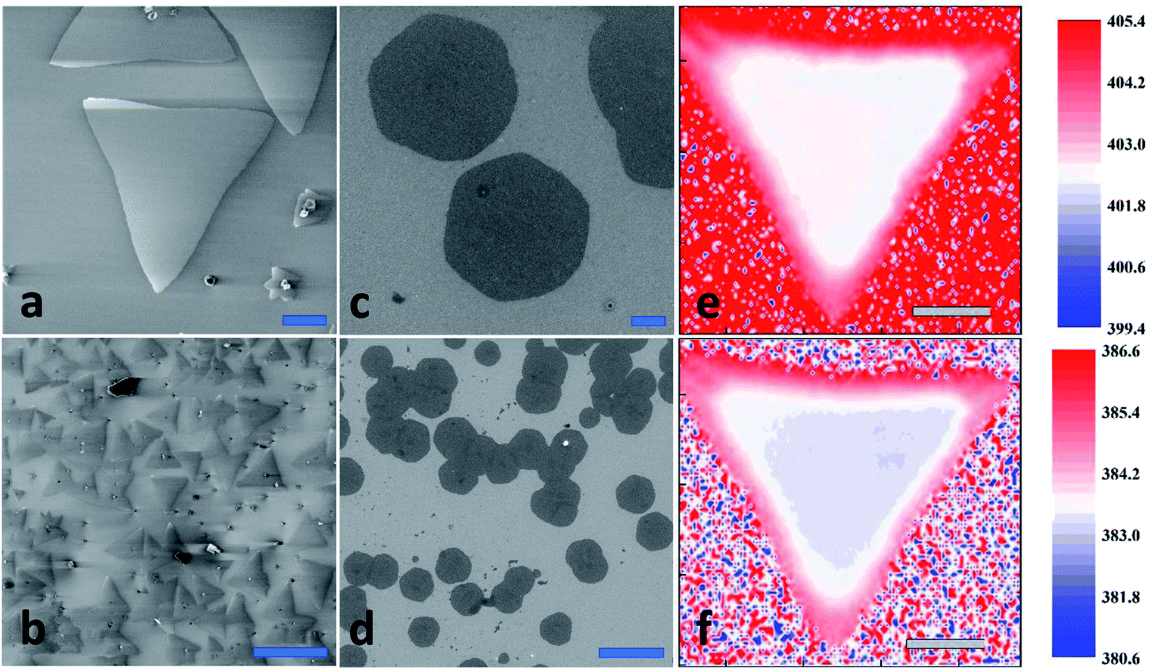 | ||
| Fig. 1 (a and b) Helium Ion Microscopy of as-grown MoS2; (c and d) SEM images of MoS2 transferred to conductive substrate for CAFM characterization; Raman map of 1LMoS2: (f) E2g at 383 cm−1, and (e) A1g at 402 cm−1. The scale bars in (a, d, e and f) are 5 μm, in (b) 50 μm, in (c) 500 nm. | ||
MoS2 samples were irradiated in a Zeiss Helium Ion Microscope operating at accelerating voltage of 30 kV with doses of (1) 1 × 10¹³, (2) 5 × 10¹⁴, (3) 9 × 10¹⁴, (4) 1 × 10¹⁵, (5) 5 × 10¹⁵, (6) 9 × 10¹⁵, and (7) 1 × 10¹⁶ He+ ions per cm2. The exposure was performed using patterning software to raster the focused helium ion beam over a large area (up to 50 μm). A beam current of 5 pA was used for all exposures with dosage being controlled by exposure time. This resulted in the introduction of defects with inter-defect distances varying from 10.3 nm to 3.7 nm as we reported elsewhere.20 Prior to doping, MoS2 samples were placed in the middle of a CVD tube furnace and annealed at 250 °C for 1 hour. The samples were then soaked in a solution of 0.3 μmol ml−1 of 2,3,5,6-tetrafluro7,7,8,8-tetracyanoquinodimethane (F4TCNQ) in Chloroform for 12 hours, then rinsed to remove unbounded F4TCNQ as suggested in.21 Thereafter, the samples were heated on a hot plate at 100 °C for 30 minutes.
2.2 Characterization techniques
Photoluminescence (PL) and Raman spectra were recorded with a Horiba XploRa Confocal Raman Microscope at 532 nm of excitation. The laser power was kept below 0.5 mW to avoid thermal damage due to heating. Scanning Probe Microscopy was performed on an Oxford Asylum Research Atomic Force Microscope (AFM) MFP-3D Infinity.Surface potential imaging was performed in amplitude-modulated mode with conductive Si tips coated with Pt/Ir (EFM-20, NanoWorld). The Asylum's ORCA™ module was used for conductive mode (CAFM). For this characterization, we transfered MoS2 samples to a Si substrate coated with a 50 nm gold film using the wet KOH transfer method.22 The I–V curves were recorded before and after modification of the MoS2 samples, with the CAFM tip (CDT-NCHR-SPL) being engaged very gently with only a few nN of force being applied until the current signal stabilized. All above measurements were performed at ambient conditions. The X-ray Photoelectron Spectroscopy (XPS) data were obtained on a Thermo Fisher ESCALAB 250 Xi. The atomically resolved images of the MoS2 sample were recorded using the Scanning Transmission Electron Microscope Nion Ultra HAADF-STEM 100 at Oak Ridge National Laboratory.
3 Results and discussions
By adjusting proper synthesis conditions, we grew 2D MoS2 flakes with the area up to 270 μm2 as shown on Fig. 1a–d. Scanning Electron and Helium Ion Microscopy allow for visualization of shape, lateral dimensions, and homogeneity of grown MoS2 samples. However, these techniques do not provide quantitative information for the number of MoS2 layers in a single flake. Confocal Raman spectroscopy is the most popular tool for reliable identification the MoS2 layer number, as well as for doping and strain. The two prominent Raman peaks located around 402 cm−1 and 383 cm−1 assigned to the out-of-plane (A1g) and in-plane (E2g) phonon vibration modes respectively. The band separation Δf = 19 − 20 cm−1 corresponds to 1L MoS2. With the increasing number of layers, the difference Δf will also increase, for instance, Δf = 21 − 22 cm−1 corresponds to bilayer of MoS2.Our typical results of Raman mapping show spatial homogeneity of E2g (Fig. 1f) and A1g (Fig. 1e) over the MoS2 flake area: the intensity and variation for both peaks were negligible, so we have identified as grown flakes as pristine monolayers. The pristine 1L MoS2 exhibits a strong PL peak centered at 1.83 eV. However, the efficiency and broadening of MoS2 emission is far from the theoretical limits of the direct band gap semiconductor material. It is already known that p-doping can positively influence the optical properties of 1L MoS2.23–25 To prove this, we started with conducting ambient surface potential measurements using two-pass AM-KPFM on the as-grown sample. The work function value Φsample and, consequently, Fermi energy shift were calculated by equation:
| Φsample = e × VCPD − Φprobe | (1) |
26 and Fermi energy is in the middle of bandgap. The measured value for as-grown 1L MoS2 showed shift of Fermi energy towards conduction band by 450 meV (Fig. 2c) indicating intrinsic n-doping of as-grown sample. These results are in agreement with previous reports on CVD grown 2D MoS2 on Si/SiO2, and are attributed mainly to the existence of natural defects such as sulfur vacancies.27,28 As expected, a small increase in the local work function was found after incubation of as-grown sample with p-dopant F4TCNQ, such that the average Fermi energy shifted towards the center of bandgap by only 200 meV (Fig. 2b, c). According to DFT calculations,29 the F4TCNQ molecule has a relatively weak adsorption on pristine MoS2 surface. Therefore, we attribute this shift of Fermi energy to the interaction of F4TCNQ with the MoS2 defect sites as further corroborated by TEM images in ESI (Fig. S5).† To have better control over optoelectronic properties of MoS2, we propose here to combine doping and defect engineering. Our earlier work has demonstrated the ability to introduce defects by irradiating MoS2 samples using Helium Ion Microscope,20 although tuning of MoS2 optical response had not been investigated earlier.
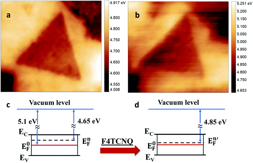 | ||
| Fig. 2 The MoS2 work function map acquired (a) before and (b) after p-doping with F4TCNQ; simplified sketch of MoS2 electronic structure before doping (c) and after doping (d). | ||
Multiple doses of Helium ion irradiation (from 1 × 10¹³ to 1 × 10¹⁶ He+ ions per cm2) were used to modify 1L MoS2 electronic structure by generating sulfur vacancies. An AFM image of the irradiated sample is presented in Fig. 3c. The high-resolution HAADF-STEM image of the sample irradiated with the dose of 1 × 10¹⁴ He+ ions per cm2 shows details of alternating symmetry of atoms arranged in hexagonal rings (Fig. 3a red arrows). Over this area, four defect sites are seen that would be available for adsorption and doping. There is also a MoS2 grain boundary that is stitching together three parts of the 1L MoS2 flake. Notably, there are no sulfur vacancies associated with broken symmetry near the grain boundaries.
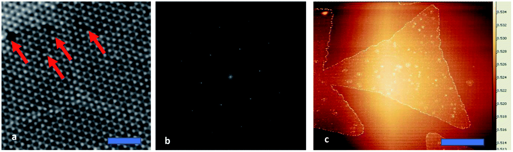 | ||
| Fig. 3 The 1L MoS2 irradiated at 1 × 10¹⁴ He+ ions per cm2 dose. (a) HAADF-STEM image; scale bar is 4 nm; the red arrows indicate single and double sulfur terminations. (b) Fourier transform of STEM image. (c) AFM topography; scale bar is 4 μm. | ||
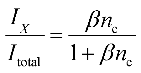
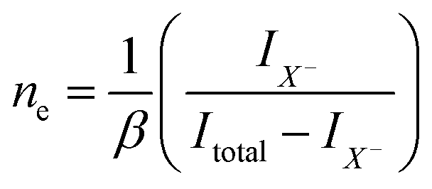
Despite of the fact, that the Fourier Transform of the STEM image (Fig. 3b) confirms preserved of the Brillouin zones hexagonal geometry, PL intensity of this sample decreased by 30%, and for the next dose it dropped down further by 60% when compared to pristine 1L MoS2 sample (Fig. 4a black-red-blue curves). To calculate the carrier concentration in the as-grown, defected, and defected-doped sample we applied the Mass Action model as introduced by J. Ross et al.30 for a three level system.14 According to this model, the relations between concentrations of excitons (NX), trions (NX−) and the excess electrons (ne) in transition metal dichalcogenides can be written as:
 | (2) |
 is related to the excess electron concentration ne:
 | (3) |
 | (4) |
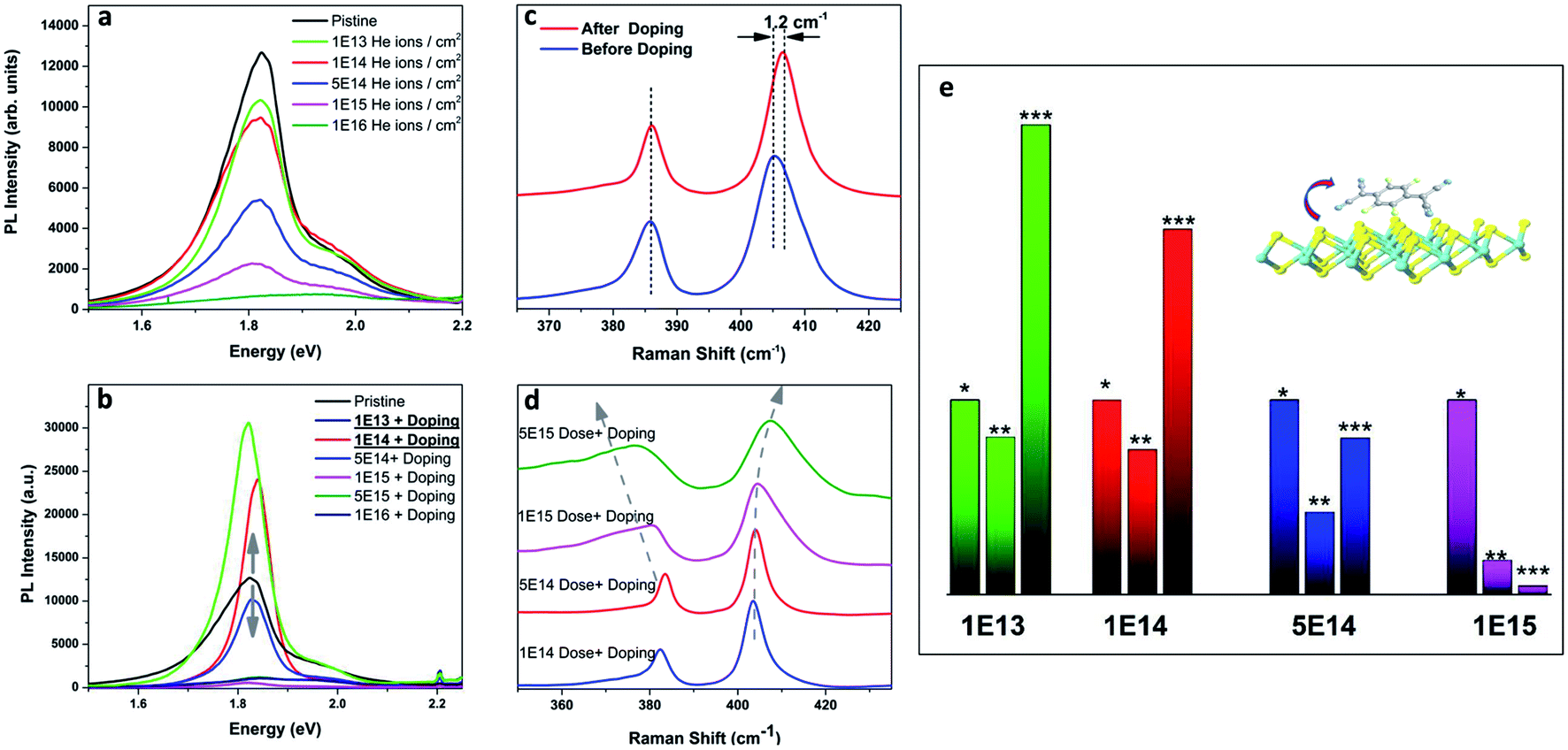 | ||
| Fig. 4 (a) MoS2 PL degradation with an increase of ion irradiation dose; and (c) Raman spectra before and after F4TCNQ doping (no ion irradiation) (b and d) PL and Raman spectra defected and doped MoS2; (e) PL Intensity of pristine (*), defected (**), and defected and doped (***) MoS2. Doses 1 × 10¹³ and 1 × 10¹⁴ provide perfect bandgap recovery and PL enhancement. | ||
We found that the trion PL weight in irradiated samples increases from 0.38 to 0.46 and correspondingly electron concentration of doped 1L MoS2 increases from 1.56 × 10¹³ 1 cm−2 to 2.2 × 10¹² 1 cm−2 (Table 1). Indeed, 1 × 10¹⁴ dose causes negligible damage. In contrast, 1 × 10¹⁶ dose disrupts MoS2 lattice symmetry completely.
| Applied doses (ions per cm2) | Trion weight | Electr. conc. (cm−2) |
|---|---|---|
| 0 | 0.38 | 1.56 × 10¹³ |
| 1 × 10¹³ | 0.383 | 1.53 × 10¹³ |
| 1 × 10¹⁴ | 0.390 | 1.62 × 10¹³ |
| 5 × 10¹⁴ | 0.410 | 1.72 × 10¹³ |
| 1 × 10¹⁵ | 0.460 | 2.2 × 10¹³ |
A simple and effective chemical p-doping method was used to tune the carrier concentration in 1L MoS2. The F4TCNQ molecule can easily bind to the sulfur vacancies and act as an acceptor. As we discussed above, Raman spectroscopy could be used to trace the doping effect in 1L MoS2. In the case of p-doping, frequency of E2g peak should remain constant, but the frequency of A1g peak is blue-shifted.32,33 Raman characterization of the F4TCNQ doped as-grown sample (untreated with ion beam) shows that the A1g peak position shifts by 1.2 cm−1 while E2g peak position remains the same (Fig. 4c). However, after irradiation, E2g/A1g modes are both red/blue shifted, and widened due to the appearance of new phonon modes. There is a shoulder (at 362 cm−1) to the left of E2g mode, and one (at 415 cm−1) to the right of A1g mode, which are assigned to a defect mode.33–35 Both peaks are significantly enhanced after irradiation with helium ions.
After p-doping of defected samples, we observe a gigantic enhancement of MoS2 PL for the dose of 1 × 10¹³ and 1 × 10¹⁴ (compare green and red curves in Fig. 4a and b), and PL recovery for the dose 5 × 10¹⁴ (blue curves in Fig. 4a and b). There is no PL recovery for the doses 1 × 10¹⁵ and higher. We attribute it to substantial damage in the MoS2 lattice by the ion bombardment. The spectral shape of the PL peak is also changing with dosage. It slightly shifts towards visible range with increase of dosage (from 1.83 eV to 1.81 eV) due to decrease of the trion weight. It is slightly lower than reported for p-doped pristine 1L MoS2 previously.14
We apply the Mass Action model to calculate carrier concentration after defect engineering and doping. Excess electron concentration decreased in comparison to the pristine sample from 1.56 to 1.13 × 1013 cm−2 (Table 2). Fig. 4e presents data for pristine, defect, and defect-doped samples. One can see that PL efficiency is increased for the 1 × 10¹³ sample by 230% and for the 1 × 10¹⁴ sample by 90%. We attribute it to a sufficient reduction of excess electron concentration and as a result, increase of exciton oscillator strength.
| Applied doses (ions per cm2) | Trion weight | Electr. conc. (cm−2) |
|---|---|---|
| 1 × 10¹³ | 0.370 | 1.40 × 10¹³ |
| 1 × 10¹⁴ | 0.306 | 1.13 × 10¹³ |
| 5 × 10¹⁴ | 0.310 | 1.12 × 10¹³ |
For I–V characterization, 1L MoS2 was transferred on the conductive substrate (Fig. 5a). The XPS characterization confirmed elemental composition Mo:S – 1:2 (Fig. 5b). The bias applied to the sample caused current flow into the conductive AFM tip, which was then recorded by a current amplifier. Fig. 4c shows the I–V graphs of as-grown, irradiated, and irradiated-doped 1L MoS2 measured by CAFM. The CAFM voltage was in the range of −1 V to 1 V. All samples: as-grown, doped, and defected and doped exhibited a clear non-linear slope of the I–V curve, which is characteristic of a metal/semiconductor junction. A clear difference is observed between the I–V curves recorded on a pristine, irradiated, irradiated-doped samples. Particularly, in the forward bias regime, higher current response is measured at the same voltage (−0.65 V) for the irradiated compared to the as-grown and irradiated-doped MoS2. After irradiation at ion dose of 1 × 10¹⁴ and doping, defected-doped 1L MoS2 showed a characteristic I–V curve of an ideal Schottky diode compared to the as-grown sample and irradiated MoS2 sample. The results of transport measurements are consistent with the Raman and Photoluminescence characterization confirming that the F4TCNQ molecules in solution can strongly withdraw electrons from MoS2 layers.
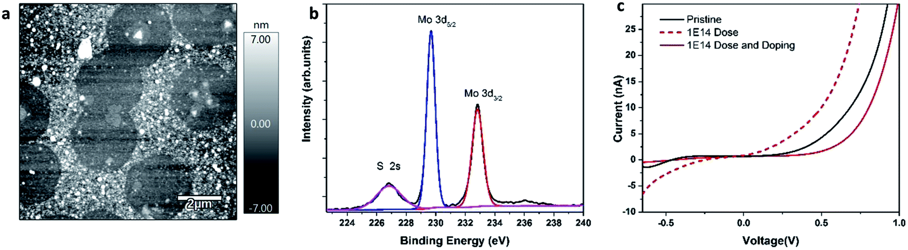 | ||
| Fig. 5 (a) AFM topography of transferred MoS2 on conductive substrate; (b) XPS core-level spectra of molybdenum 3d and sulfur 2 s; (c) I–V characterization for pristine and doped, defected and doped MoS2. | ||
4 Conclusions
In conclusion, we performed a systematic modification of the electronic structure of 1L MoS2 by (a) gentle defect introduction using helium ion microscope with doses ranging from 1 × 10¹³ to 1 × 10¹⁶ ion per cm2, and (b) subsequent p-doping of defected MoS2 sites. Reduced PL intensity was restored and drastically enhanced due to the adsorption of p-type dopants (F4TCNQ molecules) by 1L MoS2. We explain the MoS2 bandgap recovery is due to decrease of excess electron concentration resulting in an increase of exciton oscillator strength. Our findings can be useful for improvement in the efficiency of light emission devices based on two-dimensional materials beyond MoS2.Conflicts of interest
There are no conflicts to declare.Acknowledgements
Part of this work was performed at the Joint School of Nanoscience and Nanoengineering (JSNN), a member of the Southeastern Nanotechnology Infrastructure Corridor (SENIC) and National Nanotechnology Coordinated Infrastructure (NNCI), which is supported by the National Science Foundation (Grant ECCS-1542174). Some MoS2 samples for this publication was provided by The Pennsylvania State University Two-Dimensional Crystal Consortium – Materials Innovation Platform (2DCC-MIP), which is supported by NSF cooperative agreement DMR-1539916. Scanning Transmission Electron Microscope (STEM) imaging was conducted at the Center for Nanophase Materials Sciences, which is a DOE Office of Science User Facility.References
- A. K. Geim and K. S. Novoselov, Nat. Mater., 2007, 6, 183–191 CrossRef CAS PubMed.
- W. Choi, N. Choudhary, G. H. Han, J. Park, D. Akinwande and Y. H. Lee, Mater. Today, 2017, 20, 116–130 CrossRef CAS.
- S. Manzeli, D. Ovchinnikov, D. Pasquier, O. V. Yazyev and A. Kis, Nat. Rev. Mater., 2017, 2, 17033 CrossRef CAS.
- B. M. Bersch, S. M. Eichfeld, Y.-C. Lin, K. Zhang, G. R. Bhimanapati, A. F. Piasecki, M. Labella and J. A. Robinson, 2D Materials, 2017, 4, 025083 CrossRef.
- K. F. Mak, C. Lee, J. Hone, J. Shan and T. F. Heinz, Phys. Rev. Lett., 2010, 105, 136805 CrossRef PubMed.
- D. Jariwala, V. K. Sangwan, L. J. Lauhon, T. J. Marks and M. C. Hersam, ACS Nano, 2014, 8, 1102–1120 CrossRef CAS PubMed.
- P. K. Chow, R. B. Jacobs-Gedrim, J. Gao, T.-M. Lu, B. Yu, H. Terrones and N. Koratkar, ACS Nano, 2015, 9, 1520–1527 CrossRef CAS PubMed.
- J. Li, S. Hu, S. Wang, H. Kang, Z. Chen, S. Zhao, Y. Zhang, Y. Sui and G. Yu, Mater. Lett., 2021, 290, 129421 CrossRef CAS.
- M. Erementchouk, M. A. Khan and M. N. Leuenberger, Phys. Rev. B, 2015, 92, 121401 CrossRef.
- H. M. Oh, G. H. Han, H. Kim, J. J. Bae, M. S. Jeong and Y. H. Lee, ACS Nano, 2016, 10, 5230–5236 CrossRef CAS PubMed.
- B. Chen, H. Sahin, A. Suslu, L. Ding, M. I. Bertoni, F. M. Peeters and S. Tongay, ACS Nano, 2015, 9, 5326–5332 CrossRef CAS PubMed.
- T. Völzer, F. Fennel, T. Korn and S. Lochbrunner, Phys. Rev. B, 2021, 103, 045423 CrossRef.
- S. Tongay, J. Zhou, C. Ataca, J. Liu, J. S. Kang, T. S. Matthews, L. You, J. Li, J. C. Grossman and J. Wu, Nano Lett., 2013, 13, 2831–2836 CrossRef CAS PubMed.
- S. Mouri, Y. Miyauchi and K. Matsuda, Nano Lett., 2013, 13, 5944–5948 CrossRef CAS PubMed.
- T. Granzier-Nakajima, K. Fujisawa, V. Anil, M. Terrones and Y.-T. Yeh, Nanomaterials, 2019, 9, 425 CrossRef CAS PubMed.
- D. Pierucci, H. Henck, Z. Ben Aziza, C. H. Naylor, A. Balan, J. E. Rault, M. G. Silly, Y. J. Dappe, F. Bertran, P. Le Fèvre, F. Sirotti, A. T. C. Johnson and A. Ouerghi, ACS Nano, 2017, 11, 1755–1761 CrossRef CAS PubMed.
- A. Molle, F. Fabbri, D. Campi, A. Lamperti, E. Rotunno, E. Cinquanta, L. Lazzarini, D. Kaplan, V. Swaminathan, M. Bernasconi, M. Longo and G. Salviati, Adv. Electron. Mater., 2016, 2, 1600091 CrossRef.
- Y. Cai, H. Zhou, G. Zhang and Y.-W. Zhang, Chem. Mater., 2016, 28, 8611–8621 CrossRef CAS.
- M. Yarali, Y. Zhong, S. N. Reed, J. Wang, K. A. Ulman, D. J. Charboneau, J. B. Curley, D. J. Hynek, J. V. Pondick, S. Yazdani, N. Hazari, S. Y. Quek, H. Wang and J. J. Cha, Adv. Electron. Mater., 2021, 7, 2000873 CrossRef CAS.
- F. Aryeetey, T. Ignatova and S. Aravamudhan, RSC Adv., 2020, 10, 22996–23001 RSC.
- D. M. Sim, M. Kim, S. Yim, M.-J. Choi, J. Choi, S. Yoo and Y. S. Jung, ACS Nano, 2015, 9, 12115–12123 CrossRef CAS PubMed.
- H. Van Ngoc, Y. Qian, S. K. Han and D. J. Kang, Sci. Rep., 2016, 6, 33096 CrossRef PubMed.
- K. H. Kim, K. S. Kim, Y. J. Ji, I. Moon, K. Heo, D.-H. Kang, K. N. Kim, W. J. Yoo, J.-H. Park and G. Y. Yeom, J. Mater. Chem. C, 2020, 8, 1846–1851 RSC.
- K. Cho, M. Min, T.-Y. Kim, H. Jeong, J. Pak, J.-K. Kim, J. Jang, S. J. Yun, Y. H. Lee, W.-K. Hong and T. Lee, ACS Nano, 2015, 9, 8044–8053 CrossRef CAS PubMed.
- J. Yang, H. Kawai, C. P. Y. Wong and K. E. J. Goh, J. Mater. Chem. C, 2019, 123, 2933–2939 CAS.
- L. Britnell, R. M. Ribeiro, A. Eckmann, R. Jalil, B. D. Belle, A. Mishchenko, Y.-J. Kim, R. V. Gorbachev, T. Georgiou, S. V. Morozov, A. N. Grigorenko, A. K. Geim, C. Casiraghi, A. H. C. Neto and K. S. Novoselov, Science, 2013, 340, 1311–1314 CrossRef CAS PubMed.
- I. Sharma and B. R. Mehta, J. Alloys Compd., 2017, 723, 50–57 CrossRef CAS.
- W. H. Chae, J. D. Cain, E. D. Hanson, A. A. Murthy and V. P. Dravid, Appl. Phys. Lett., 2017, 111, 143106 CrossRef.
- O. K. Le, V. Chihaia, V. Van On and D. N. Son, RSC Adv., 2021, 11, 8033–8041 RSC.
- J. S. Ross, S. Wu, H. Yu, N. J. Ghimire, A. M. Jones, G. Aivazian, J. Yan, D. G. Mandrus, D. Xiao, W. Yao and X. Xu, Nat. Commun., 2013, 4, 1474 CrossRef PubMed.
- K. F. Mak, K. He, C. Lee, G. H. Lee, J. Hone, T. F. Heinz and J. Shan, Nat. Mater., 2013, 12, 207–211 CrossRef CAS PubMed.
- B. Chakraborty, A. Bera, D. V. S. Muthu, S. Bhowmick, U. V. Waghmare and A. K. Sood, Phys. Rev. B, 2012, 85, 161403 CrossRef.
- H. Li, Q. Zhang, C. C. R. Yap, B. K. Tay, T. H. T. Edwin, A. Olivier and D. Baillargeat, Adv. Funct. Mater., 2012, 22, 1385–1390 CrossRef CAS.
- S. Mignuzzi, A. J. Pollard, N. Bonini, B. Brennan, I. S. Gilmore, M. A. Pimenta, D. Richards and D. Roy, Phys. Rev. B, 2015, 91, 195411 CrossRef.
- Y. Chen, S. Huang, X. Ji, K. Adepalli, K. Yin, X. Ling, X. Wang, J. Xue, M. Dresselhaus, J. Kong and B. Yildiz, ACS Nano, 2018, 12, 2569–2579 CrossRef CAS PubMed.
Footnote |
| † Electronic supplementary information (ESI) available. See DOI: 10.1039/d1ra02888j |
| This journal is © The Royal Society of Chemistry 2021 |