
 Open Access Article
 This Open Access Article is licensed under a
 Creative Commons Attribution 3.0 Unported Licence
Morphology and surface analyses for CH3NH3PbI3 perovskite thin films treated with versatile solvent–antisolvent vapors
Nasir Awolab,
Chernet Amentec,
Gaurav Verma *bd and
Jung Yong Kim*ae
*bd and
Jung Yong Kim*ae
aSchool of Materials Science and Engineering, Jimma Institute of Technology, Jimma University, P. O. Box 378, Jimma, Ethiopia. E-mail: jungyong.kim@ju.edu.et
bDr Shanti Swarup Bhatnagar University Institute of Chemical Engineering and Technology, Panjab University, Chandigarh, 160014, India. E-mail: gauravverma@pu.ac.in
cDepartment of Physics, College of Computational and Natural Science, Addis Ababa University, P. O. Box 1176, Addis Ababa, Ethiopia
dCentre for Nanoscience & Nanotechnology, University Institute for Emerging Areas in Science and Technology, Panjab University, Chandigarh, 160014, India
eSchool of Chemical Engineering, Jimma Institute of Technology, Jimma University, P. O. Box 378, Jimma, Ethiopia
First published on 17th May 2021
Abstract
Organometal halide perovskite (CH3NH3PbI3) semiconductors have been promising candidates as a photoactive layer for photovoltaics. Especially for high performance devices, the crystal structure and morphology of this perovskite layer should be optimized. In this experiment, by employing solvent–antisolvent vapor techniques during a modified sequential deposition of PbI2–CH3NH3I layers, the morphology engineering was carried out as a function of antisolvent species such as: chloroform, chlorobenzene, dichlorobenzene, toluene, and diethyl ether. Then, the optical, morphological, structural, and surface properties were characterized. When dimethyl sulfoxide (DMSO, solvent) and diethyl ether (antisolvent) vapors were employed, the CH3NH3PbI3 layer exhibited relatively desirable crystal structures and morphologies, resulting in an optical bandgap (Eg) of 1.61 eV, crystallite size (t) of 89.5 nm, and high photoluminescence (PL) intensity. Finally, the stability of perovskite films toward water was found to be dependent on the morphologies with defects such as grain boundaries, which was evaluated through contact angle measurement.
1. Introduction
Organometal halide perovskite solar cells (PSCs) have received tremendous interest for a next-generation photovoltaic (PV) technology.1–5 Perovskite can be designated by a common formula known as ABX3 where ‘A’ is a large organic cation [CH3NH3 or HC (NH2)2], ‘B’ is a metal cation (Pb, Sn), and ‘X’ is a halide (Cl, Br, I). The perovskite material is a light-harvesting component of the PSCs, and is able to offer many desirable characteristics such as low-temperature solution processability,6,7 high absorption coefficient,8 long carrier diffusion length,9 high charge carrier mobility,10 and adjustable direct bandgap with suitable alternative metals, halogens, and organic cations.11–14 These characteristics can be further modified by using additives,15–17 compositional adjustments,18,19 and solvent–antisolvent extraction approaches.20 Hence, the PSCs have been a promising candidate for commercialization in the current PV industries.In general, the PV performance of PSCs relies on the morphologies of the perovskite thin film because the structural characteristics of a photoactive layer decide PV performances of devices.21–32 For example, if there is a trap site (e.g., surface defect and grain boundary) in a perovskite layer, it acts as carrier recombination sites,33 resulting in a reduced performance of devices. Thus, the morphology and crystallinity of the perovskite thin film should be very important for fabricating high-efficiency PV devices.34
To date, numerous approaches have been developed to obtain a high quality and defect-minimized perovskite thin film.35,36 For example, thermal annealing of a perovskite film at 85–120 °C has been employed.37 Furthermore, low-temperature antisolvent assisted fabrication of devices are one of the useful techniques for obtaining a film with desired morphologies.18,19 Importantly, it is notable that the additive and antisolvent strategies are both significantly promising in improving the performance of PSCs.38–49 Moreover, the dipping time,50 precursor's type and concentration,51 spin-speed,52 solvent types,53,54 and temperature are important processing factors for optimizing a perovskite layer. In the sequential deposition of the PbI2 and CH3NH3I (MAI) layers, the MAI's intercalation into the PbI2 layer is critically important to obtain a high quality perovskite without any unreacted precursor material. If there is an incomplete conversion of PbI2–MAI into a perovskite, it may be a problem for device performances.55 However, for improving the stability of PSCs, there are researchers who used a PbI2 interfacial nanolayer in their device configuration.56–60
In this work, we employed a modified sequential deposition method for fabricating organometal halide perovskite thin films. For this purpose, the solvent–antisolvent vapor techniques were adopted as a method of morphology engineering. The five anti-solvents such as chloroform (CF), chlorobenzene (CB), 1,2-dichlorobenzene (DCB), toluene (Tol), and diethyl ether (Et2O) were tested, which may act as an extractor of a solvent, dimethyl sulfoxide (DMSO). Then the properties of CH3NH3PbI3 thin films were investigated as a function of antisolvent species, which may include UV-vis light absorption, micro-/nano-structural morphologies, crystal structures, photoluminescence (PL) emission, and surface analysis through the water contact-angle measurements. In this study, it was observed that when a perovskite layer is well crystallized, the surface polarity of perovskite films remains a longer time, i.e., an enhanced stability toward water or its vapor.
2. Experimental section
2.1. Materials and methods
In all synthesis methods, analytical grade high purity reagents were used. All solvents and antisolvents were purchased from Fine Chemicals Ltd. Indium tin oxide/fluorine-doped tin oxide (ITO/FTO) coated glass substrates were purchased from TECHINSTRO Chemicals Ltd. PbI2 precursors were purchased from Tokyo chemical industries (TCI) and synthesized using a hydrothermal method.27 CH3NH3I (MAI) was synthesized by reacting methylamine (aqueous, 40 wt%) and hydroiodic acid (aqueous, 57 wt%) in an ice bath for 2 h with stirring. Then the solvent was evaporated using a rotary evaporator and the precipitate was collected and washed using Et2O three times and dried at 60 °C for 24 h in a vacuum oven. The resulting product, MAI, was used without further purification. To obtain a CH3NH3PbI3 precursor, the synthesized PbI2 and MAI were deposited on the top of poly(3,4-ethylenedioxythiophene):polystyrene sulfonate (PEDOT:PSS)-coated substrate using a modified sequential deposition technique: (a) PbI2/DMSO deposition, (b) MAI/IPA deposition at a 1![[thin space (1/6-em)]](https://www.rsc.org/images/entities/char_2009.gif) :1 mole ratio, and (c) solvent–antisolvent exposure, in which the solvent is DMSO, and the antisolvents are CF, CB, DCB, Tol, and Et2O.
:1 mole ratio, and (c) solvent–antisolvent exposure, in which the solvent is DMSO, and the antisolvents are CF, CB, DCB, Tol, and Et2O.
2.2. Thin-film preparation
To study the effect of a solvent, DMSO was used to prepare 1 M of PbI2 (461.78 mg ml−1 of DMSO) solution and annealed at 80 °C for 12 hours. ITO coated glass substrates were used to deposit the samples and sequentially washed with detergent, DI water, and ethanol in an ultrasonic bath. A hole transporting material PEDOT:PSS was deposited on the top of the ITO glass substrate. Then, the PbI2 precursor solution was filtered by a 2 μm sterile polytetrafluoroethylene (PTFE) membrane filter. PbI2/DMSO was spin-coated on the top of the PEDOT:PSS layer and heated at a temperature of 100 °C. Then, the as-synthesized MAI in isopropyl alcohol (IPA) solution was spin-coated on the top of the PbI2 layer. After deposition of the MAI, the thin film was exposed to a DMSO vapor at 80 °C for 10 minutes, and then the crystallizable perovskite layer was exposed to different antisolvent vapor at 70 °C for 10 minutes. The optical, structural, morphological, and surface properties of organometal halide perovskite thin films were then investigated, accordingly.2.3 Characterization
UV-visible spectra measurements were taken on thin films using Shimadzu UV-2600-Series, diffused reflectance spectrophotometer double-beam source at a range of 350–800 nm fitted with deuterium and halogen lamps as sources. Transmission and reflection modes were recorded simultaneously. ITO glasses have been used as a background reference for thin films. The X-ray diffraction (XRD) patterns of the as-prepared perovskite samples have been characterized by Philips X'pert PRO-240 mm diffractometer provided with an integrated germanium detector Cu-Kα, radiation source at λ = 1.54060 Å operating at an applied voltage of 45 kV with a current intensity of 40 mA. The equatorial scans in the continuous mode were taken from 2θ = 4° to 80° at a step of 0.017° with a scan step time of 24.4 seconds. To probe the electron transition behavior of samples photoluminescence (PL) spectroscopy was utilized by F-7000 fluorescence spectrophotometer, Hitachi, Japan, using a xenon lamp at a wavelength of 532 nm with an emission wavelength starting from 600 nm to 850 nm at a scan speed of 1200 nm min−1. The morphologies of perovskite films were investigated by field-emission scanning electron microscopy (FE-SEM; Hitachi, Japan, SU8000 Series) at an accelerating voltage of 5.0 kV. Energy-dispersive X-ray spectroscopy (EDX) investigation has been performed to probe the elemental distribution variations present in the thin film. Mapping analysis has been done to obtain elemental maps in the range of nanoscale. Contact Angle Goniometer (KRUSS GmbH, DSA25; Germany) was used to record and analyze the effect of antisolvents on the surface energies of perovskite thin films. To determine contact angle, the edge detection of the water droplet was fitted by a polynomial fitting approach. Measurements were taken in time intervals of 40 ms over a period of 30 seconds.3. Results and discussion
Fig. 1(a) shows a modified sequential deposition of the perovskite layer. For the first step, PbI2 is deposited on the top of PEDOT:PSS/ITO substrate, then, the MAI is spin coated on the top of PbI2/PEDOT:PSS/ITO. Finally, the solvent (DMSO) and antisolvent (CF, CB, DCB, Tol, Et2O) vapors are sequentially exposed to the perovskite layer. The properties of solvent and antisolvents were summarized in Table 1. Here, the solubility parameter (δ) with the dimension of (cal cm−3)1/2 is in the order of 14.5 (DMSO) > 10 (DCB) > 9.5 (CB) > 9.2 (CF) > 8.9 (Tol) > 7.4 (Et2O), indicating that DMSO is the most polar, whereas Et2O is the most nonpolar. Furthermore, the boiling point (bp) is in the order of 189 °C (DMSO) > 180 °C (DCB) > 131 °C (CB) > 111 °C (Tol) > 61 °C (CF) > 35 °C (Et2O), displaying Et2O is the most volatile.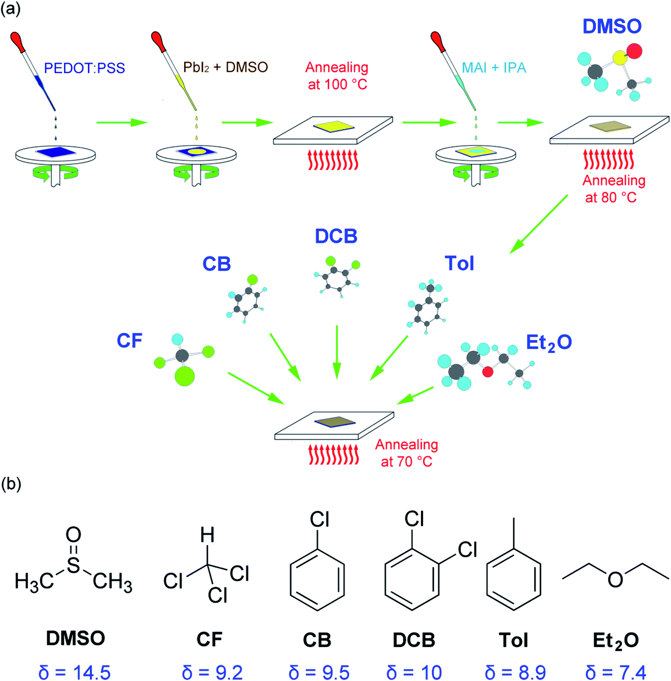 | ||
| Fig. 1 (a) A modified sequential deposition technique for perovskite film, for which a solvent–antisolvent vapor-exposure technique was employed for morphology engineering. (b) Chemical structures of solvent and antisolvents for organometal halide perovskites. Here δ is the solubility parameter with a dimension of (cal cm−3)1/2. | ||
| Molecule | Chemical formula | δa (cal cm−3)1/2 | δ MPa1/2 | MW (g mol−1) | ρ (g cm−3) | bp (°C) |
|---|---|---|---|---|---|---|
| a In the text, the dimension of (cal cm−3)1/2 was used for solubility parameter. | ||||||
| DMSO | C2H6OS | 14.5 | 29.71 | 78.13 | 1.10 | 189 |
| CF | CHCl3 | 9.2 | 18.85 | 119.38 | 1.49 | 61 |
| CB | C6H5Cl | 9.5 | 19.47 | 112.56 | 1.11 | 131 |
| DCB | C4H4Cl2 | 10.0 | 20.49 | 147.01 | 1.30 | 180 |
| Tol | C7H8 | 8.9 | 18.24 | 92.14 | 0.87 | 111 |
| Et2O | C4H10O | 7.4 | 15.16 | 74.12 | 0.71 | 35 |
For solvent–antisolvent vapor engineering, the solvent/antisolvent should be miscible, whereas the perovskite/antisolvent immiscible. During the film-formation process, if the number of nucleation cites is reduced, the crystal and grain size of perovskite may increase, resulting in a high quality film with small grain boundaries. For this purpose, the solvent DMSO molecules should be quickly extracted from the wet DMSO/perovskite film by help of antisolvent.61,62 Furthermore, it is notable that although perovskite is hygroscopic and hydrophilic, the measured water-contact angle was reported to be very high (i.e., significantly hydrophobic). This paradox was solved by recognizing that the hydrophobic PbI2 is formed at the interface of water and CH3NH3PbI3.63 In other words, the measured water contact angle is not for CH3NH3PbI3, but for PbI2 (i.e., the result of a perovskite degradation). Here, of course, the contact angle data may include the effect of the morphologies of a film including grain boundaries.
Fig. 1(b) shows the chemical structure of solvent and antisolvents. Here the solubility parameter (δ) is equal to a square root of cohesive energy density (CED), i.e.,  , where Ûvap is the molar heat of vaporization, and
 ![[V with combining circumflex]](https://www.rsc.org/images/entities/i_char_0056_0302.gif) is the molar volume.64 Furthermore, two small organic molecules (here, solvent and antisolvent) are expected to be miscible because of a large entropic gain, although there is an enthalpic cost from the apparent dissimilarity in solubility parameters. Hence, ΔGmix = ΔHmix − TΔSmix < 0, in which ΔGmix, ΔHmix, andΔSmix denote the Gibbs free energy, enthalpy, and entropy of mixing, respectively, and T is temperature. On the other hand, for the intermolecular interactions between antisolvent and perovskite, the relation should be ΔGmix > 0, facilitating a wet perovskite film to undergo a drying process.
is the molar volume.64 Furthermore, two small organic molecules (here, solvent and antisolvent) are expected to be miscible because of a large entropic gain, although there is an enthalpic cost from the apparent dissimilarity in solubility parameters. Hence, ΔGmix = ΔHmix − TΔSmix < 0, in which ΔGmix, ΔHmix, andΔSmix denote the Gibbs free energy, enthalpy, and entropy of mixing, respectively, and T is temperature. On the other hand, for the intermolecular interactions between antisolvent and perovskite, the relation should be ΔGmix > 0, facilitating a wet perovskite film to undergo a drying process.
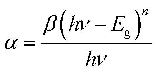
Fig. 2(a) shows the UV-vis absorption spectra of perovskite films as a function of antisolvent species. As shown in Fig. 2(a), although the overall shape of absorption is similar, the absorption edge, i.e., the optical bandgap (Eg), is a little bit different due to a non-identical ordering state of a film. Here, the absorption data was replot using the Tauc model,65
 | (1) |
 | ||
| Fig. 2 (a) UV-vis absorption spectra of the perovskite thin films as a function of nonsolvent species. (b) The plot (αhν)2 vs. hν: optical bandgaps of each perovskite film. | ||
As shown in Fig. 2(b), the plot (αhν)2 vs. hν, results in the optical bandgap of ∼1.61–1.63 eV. As an example, the absorption edge is 770.19 nm (Eg = 1.61 eV) for Et2O vapor condition, whereas it is 760.74 nm (Eg = 1.63 eV) for ‘None’ condition, i.e., the perovskite sample was not exposed to any solvent/antisolvent vapor. Here, the small bandgap indicates that the perovskite semiconductor has a well-organized structure, as observed in other stereoregular polymer semiconductors through red-shift in the absorption spectra.67–69 Note that, if the perovskite becomes a single crystalline wafer, the bandgap was reported to be much smaller like 1.36 eV, corresponding to the light absorption onset at 910 nm.70 This trend indicates that the allowed energy states of an electron increase with reducing defect densities in the crystalline lattice forming a periodic potential. In other words, the energy band increases and the bandgap decreases if the quality of perovskite films is improved. Furthermore, if there are any defects in perovskite, the typical trap energies are known to be shallow because of its defect-tolerance property.71–73 Hence, based on the optical data, the ordering of perovskite materials is in the order of: Et2O > Tol > DCB > CB > CF > ‘None’. Interestingly, if there is no solvent–antisolvent vapor treatment, the perovskite sample exhibits the smallest optical absorption, indicating that the vapor treatment is a useful technique for organizing the perovskite films.
Fig. 3 shows the SEM image for perovskite thin films as a function of antisolvent species: (a) ‘None’, (b) CF, (c) CB, (d) DCB, (e) Tol, and (f) Et2O. Interestingly, as expected from the UV-vis absorption data, (f) Et2O-vapor and (e) Tol-vapor conditions display the most organized crystal structures with three-dimensional cubic or cuboid shapes. However, (a) ‘None’ and (b) CF vapor conditions show two-dimensional flake-like structures, whereas (c) CB and (d) DCB antisolvent conditions exhibit non-uniform morphologies. Finally, if the two conditions, (e) Tol and (f) Et2O are compared each other, the latter has a better morphology with uniformity and fewer pinholes than the former as shown in Fig. 3(e) and (f), suggesting that Et2O's properties such as δ = 7.4 (cal cm−3)1/2 and bp = 34.6 °C should be helpful to extract DMSO from the wet DMSO/perovskite film.
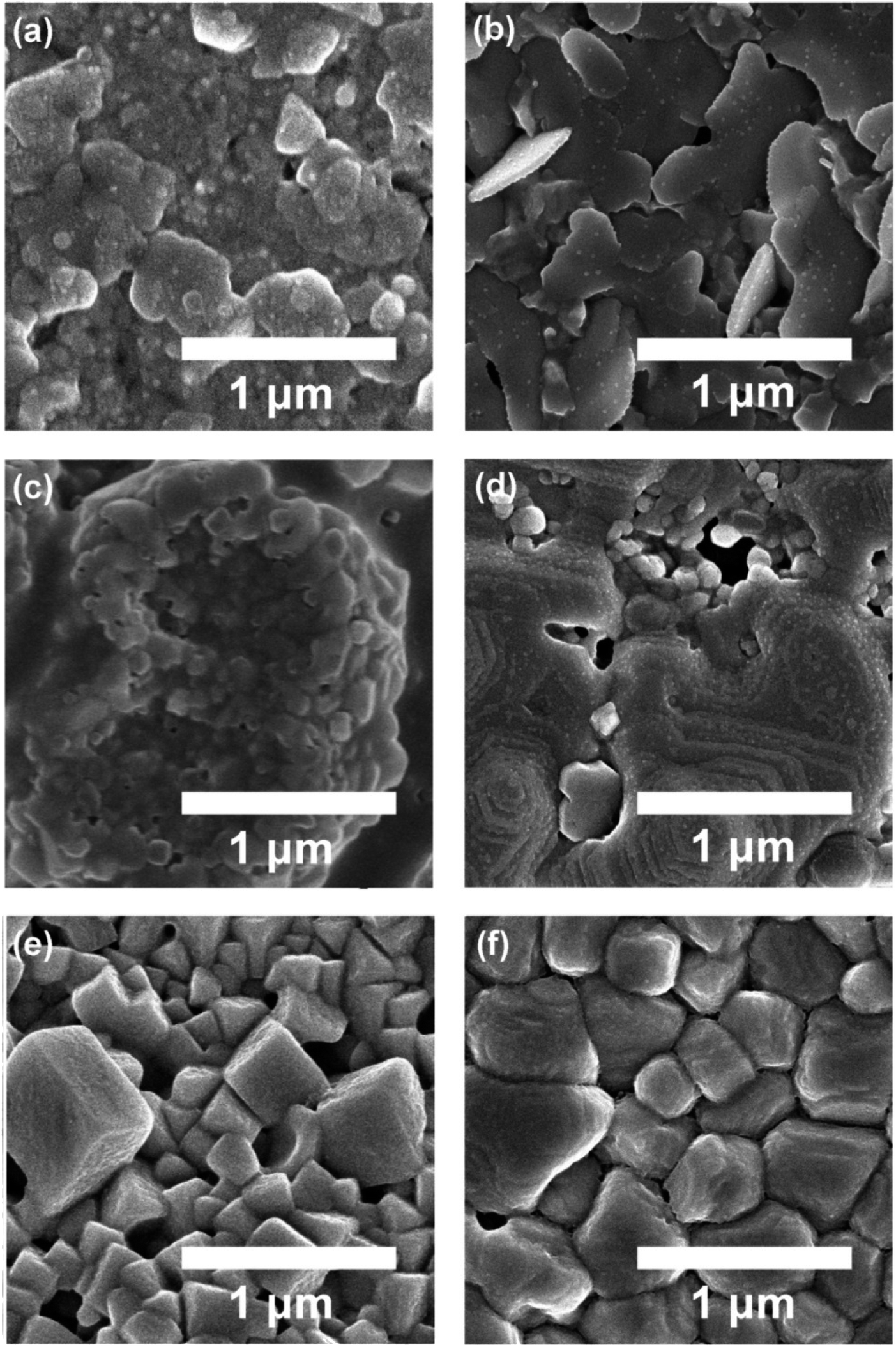 | ||
| Fig. 3 The SEM image of perovskite thin films deposited under different antisolvent conditions such as (a) ‘None’: without antisolvent, (b) CF, (c) CB, (d) DCB, (e) Tol, and (f) Et2O. | ||
Fig. 4 shows the elemental mapping images of perovskite films for the three representative cases, (a) ‘None’, (b) Tol, and (c) Et2O. Here, the mapping data follows the morphologies of a sample according to the SEM images (Fig. 3). Accordingly, Et2O-treated perovskite film shows a uniform distribution of organic/inorganic elements, whereas Tol-treated one exhibits some voids/pinholes as shown in Fig. 4.
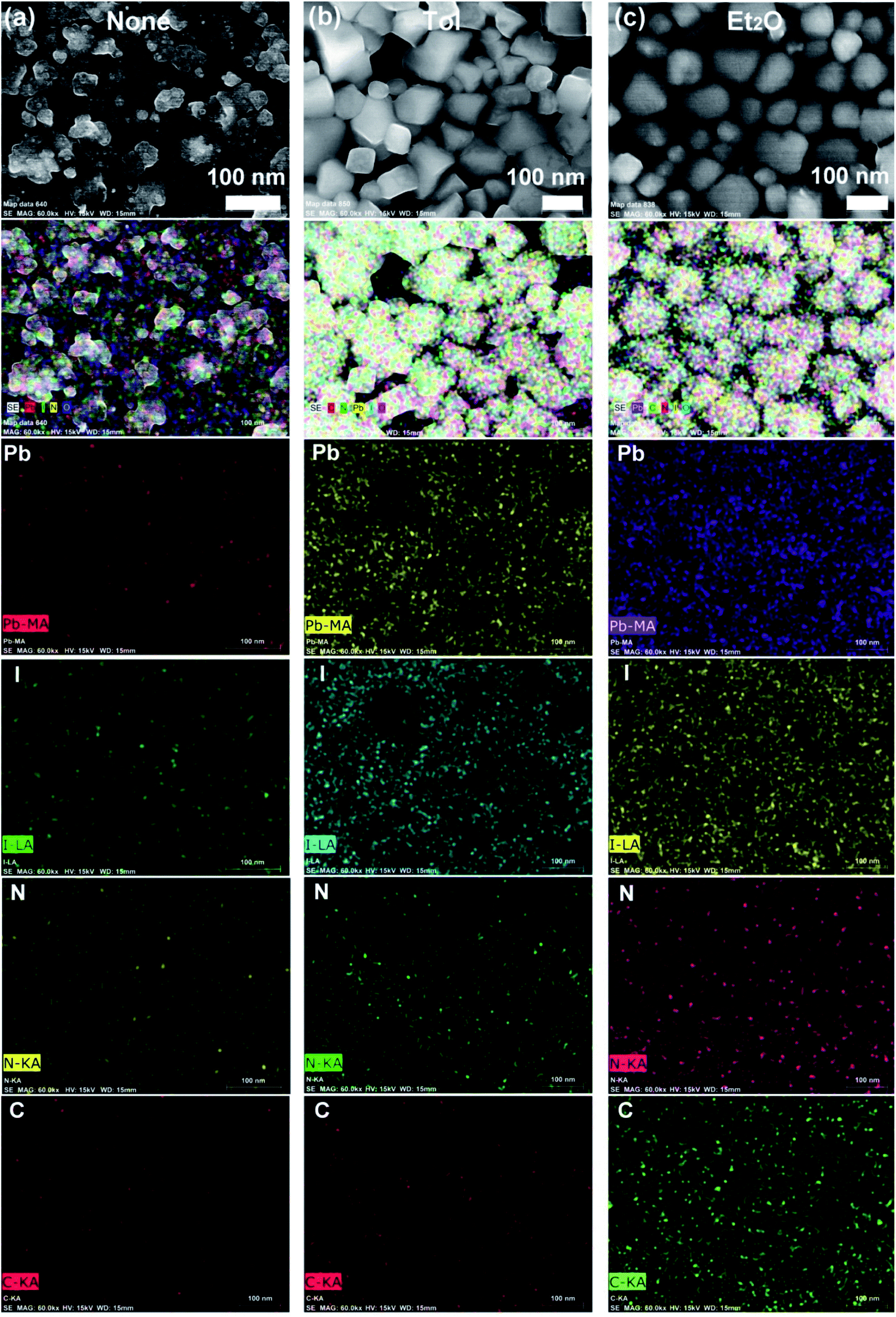 | ||
| Fig. 4 Elemental mapping images of the perovskite films according to each antisolvent condition: (a) ‘None’: without solvent–antisolvent vapors, (b) Tol, and (c) Et2O. | ||
Fig. 5(a) shows XRD patterns for the perovskite film as a function of antisolvent species at room temperature. Importantly, CH3NH3PbI3 is a polymorphic material, exhibiting the crystal structures of orthorhombic at T < 162.2 K, tetragonal at 162.2 K < T < 327.4 K, and cubic at T > 327.4 K.74 Indeed, based on the data in Fig. 5(a), the calculated lattice parameters are a = b = 8.87 Å and c = 12.65 Å, confirming that perovskite has a tetragonal structure at ∼298 K according to the literature report.75 Interestingly, in Fig. 5(a), it is noticeable that ‘None/CF/CB/DCB’ conditions display unreacted PbI2 peak at 2θ ≈ 13°,59 whereas Et2O and Tol conditions do not exhibit such a peak from unreacted PbI2. This observation indicates that, in a modified sequential deposition process, PbI2 compounds would be reacted with MAI completely when DMSO-Tol or DMSO-Et2O was used as a solvent–antisolvent couple system. This is because Et2O [δ = 7.4 (cal cm−3)1/2 and bp = 35 °C] and Tol [δ = 8.9 (cal cm−3)1/2 and bp = 111 °C] are relatively nonpolar and volatile, allowing the wet DMSO/perovskite film to be dried fast (i.e., the mixed DMSO-Tol or DMSO-Et2O molecules are quickly evaporated from the hygroscopic perovskite). This rapid crystallization results in a complete reaction between PbI2 and MAI. Furthermore, based on the most intense peak at (110) crystallographic planes in Fig. 5(a), the crystallite size of each perovskite film could be estimated. The result is displayed in Fig. 5(b). Importantly, the trend of crystallite size variation is in line with the UV-vis absorption data. However, one exception was observed in “CF’ condition which has volatile characteristics (bp = 61 °C). Recall the boiling point is in the order of 189 °C (DMSO) > 180 °C (DCB) > 131 °C (CB) > 111 °C (Tol) > 61 °C (CF) > 35 °C (Et2O). Table 2 shows the crystallite size of (110) crystallographic plane when d-spacing is 0.623 nm. Here the crystallite size (t) was calculated based on Scherrer's equation as follows,76,77
 | (2) |
sinθ).
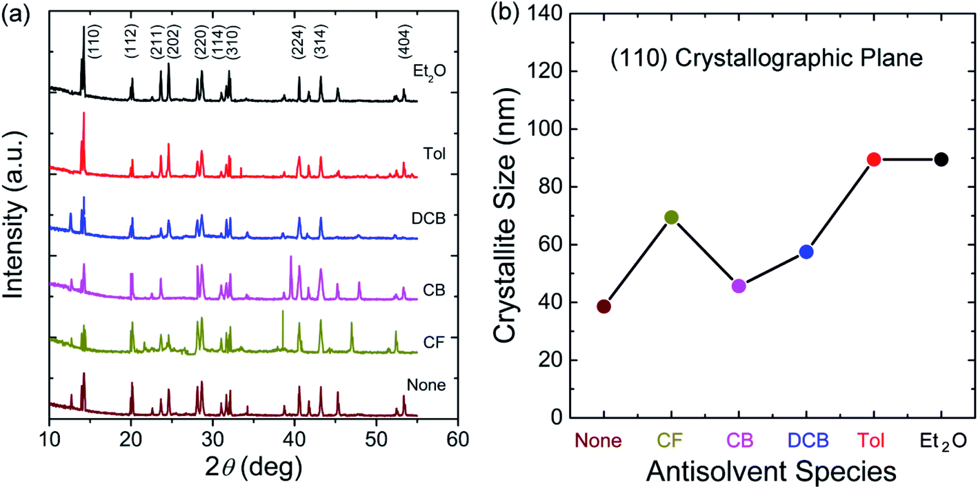 | ||
| Fig. 5 (a) XRD spectra of the perovskite thin films deposited under various antisolvent environments. (b) Crystallite size at the (110) crystallographic plane as a function of antisolvent species. | ||
| Antisolvent vapor when solvent vapor is DMSO | ||||||
|---|---|---|---|---|---|---|
| None | CF | CB | DCB | Tol | Et2O | |
| B (rad) | 0.00362 | 0.00201 | 0.00306 | 0.00243 | 0.00156 | 0.00156 |
| t (nm) | 38.6 | 69.5 | 45.6 | 57.5 | 89.5 | 89.5 |
Fig. 6 shows PL spectra for perovskite film as a function of antisolvent species, in which the peak was observed at 792.6 nm (‘None’), 792.0 nm (CF), 792.2 nm (CB), 792.5 nm (DCB), 792.6 nm (Tol), and 792.2 nm (Et2O), indicating the PL peak positions have no direct relationship with the optical bandgap (Eg) shown in Fig. 2(b). However, the PL intensity has a direct correlation with the Eg in the UV-vis absorption data. For example, when Eg is 1.61 eV (the most red-shift sample), the PL intensity is highest, indicating that, when crystallite size is large in a well-organized morphology, the radiative recombination process is carried out abundantly, resulting in the highest intensity of PL. In other words, when morphologies have a lot of defects like in ‘None’ or ‘CF’ conditions, the probability of non-radiative recombination is increased, resulting in a weak intensity of PL as proved in Fig. 6.
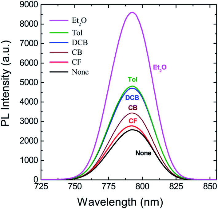 | ||
| Fig. 6 PL spectra for perovskite films as a function of antisolvent species. Note that here a perovskite film was directly deposited on the top of a glass slide (not PEDOT:PSS/ITO substrate) for the clarity of experiments. | ||
Finally, to understand the surface polarity of perovskite films depending on solvent–antisolvent vapor exposure, the water contact angle (θc: here, subscript ‘c’ stands for contact angle) was measured (see Fig. 7 and 8). Here, it should be bear in mind that, when water is dropped on the surface of perovskite film, the nanoscale PbI2 film is known to be immediately formed at the interface between water and perovskite through degradation of CH3NH3PbI3.63 However, despite this PbI2 formation, the stability of perovskite film could be studied. This is because polycrystalline morphologies contain a lot of defects such as grain boundaries through which water molecules can be easily penetrated, resulting in the change of surface polarity of a film.
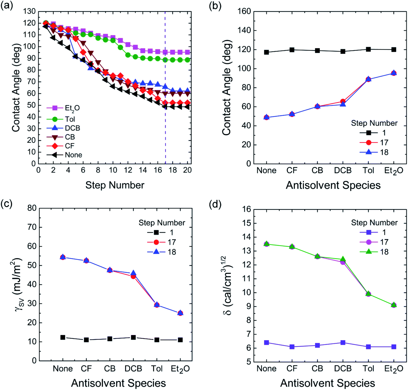 | ||
| Fig. 7 (a) Water contact angle (θc) as a function of step number for each perovskite film made by different antisolvent vapor exposure. (b) Water contact angle, (c) surface energy, and (d) solubility parameter as a function of antisolvent species when the step numbers are 1, 17, and 18. | ||
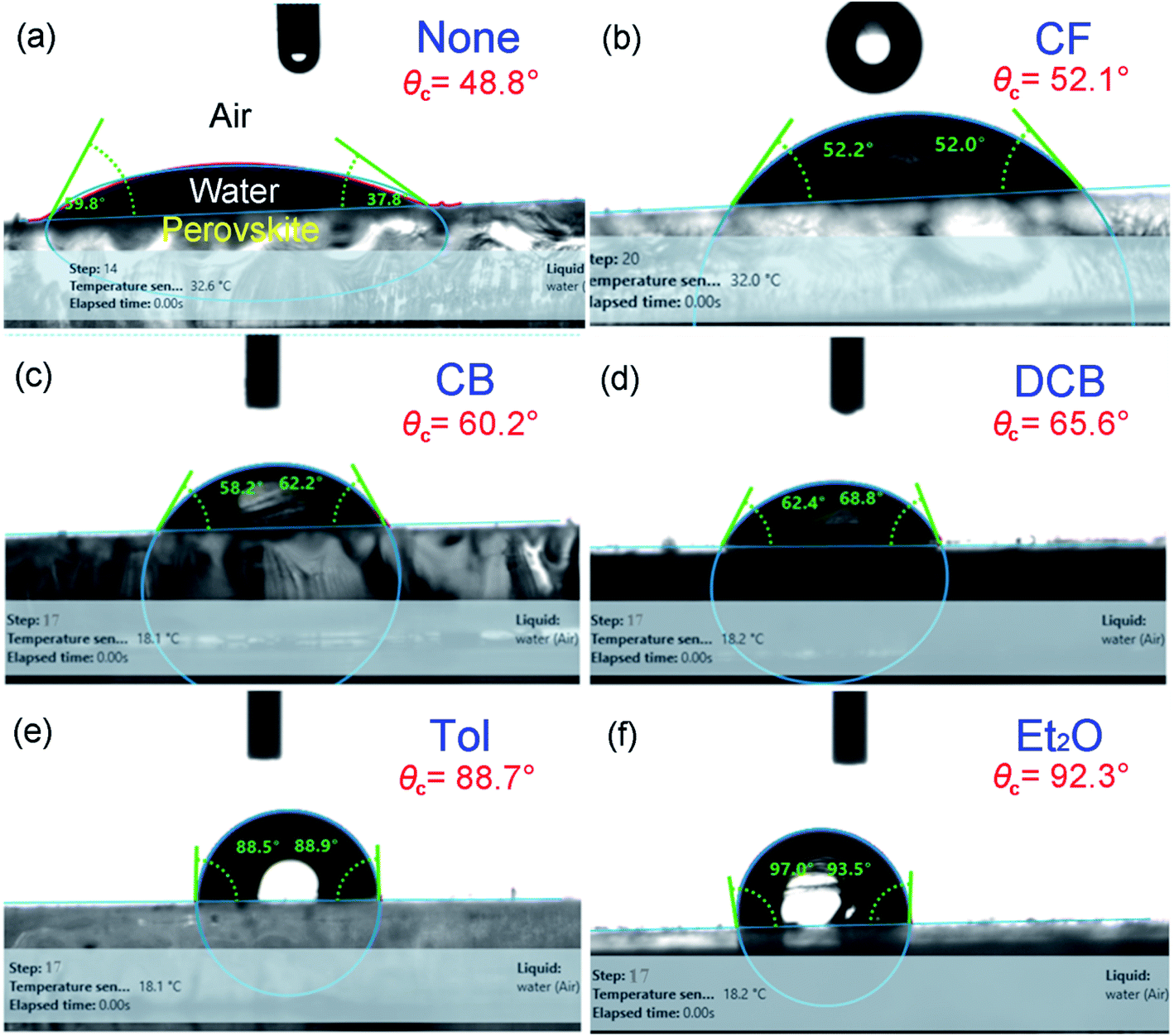 | ||
| Fig. 8 Examples of water contact angle (θc) raw data at step number 17: (a) None, (b) CF, (c) CB, (d) DCB, (e) Tol, and (f) Et2O. | ||
The raw contact-angle data at step number 17 is displayed in Fig. 8 as an example. Fig. 7(a) shows contact angle change as a function of step number in which each measurement was taken in time intervals of 40 ms over 30 s. In Fig. 7(a), the first striking observation is that, with increasing the step number, the contact angle decreased, indicating the polarity of a perovskite film was changed through the water-induced degradation effect. Note that in our previous work,27 the contact angle and surface energy for the pure PbI2 films (DMSO used as a processing solvent) were 130° and 6.3 mJ m−2, respectively. However, in this work, the perovskite film (from which PbI2 is formed, like a water/PbI2/CH3NH3PbI3 configuration) shows the water contact angle of about 120° and the average surface energy of ∼11.5 mJ m−2 (see Step 1 in Table 3). Hence, the water contact angle of a perovskite film should be affected by perovskite's degradation (PbI2), morphologies (including grain boundaries), and others.
| Antisolvent | Contact angle (°) | Surface energy (mJ m−2) | ||||
|---|---|---|---|---|---|---|
| Step 1 | Step 17 | Step 18 | Step 1 | Step 17 | Step 18 | |
| None | 117.2 | 48.8 | 48.8 | 12.3 | 54.3 | 54.3 |
| CF | 119.8 | 52.1 | 52.1 | 11.0 | 52.5 | 52.5 |
| CB | 118.9 | 60.2 | 60.2 | 11.6 | 47.5 | 47.5 |
| DCB | 118.1 | 65.6 | 62.3 | 12.3 | 44.3 | 45.9 |
| Tol | 120.3 | 88.7 | 88.7 | 11.0 | 29.3 | 29.3 |
| Et2O | 120.0 | 95.3 | 95.3 | 11.0 | 25.0 | 25.0 |
The change of water contact angle with time was smaller for the cases of Et2O and Tol compared to the others, indicating that, when the perovskite materials were well crystallized (recall Fig. 3), the stability of films (i.e., water-resistivity) should be significantly improved in humid conditions. The next observation is that at steps 17 and 18, the contact angle was saturated as shown in Fig. 7(b). In this study, it is noticeable that considering the golden triangle in solar cells (that is efficiency, stability, and cost),78 this stability-enhanced perovskite film should be important, providing a general insight for the necessity of a single crystal70 without any grain boundary as an ideal condition if there is a practical processibility.
4. Conclusion
The morphologies and surface properties of CH3NH3PbI3 thin films were studied by varying solvent–antisolvent vapor treatment conditions, for which the solvent was dimethyl sulfoxide (DMSO), and the antisolvents were chloroform (CF), chlorobenzene (CB), dichlorobenzene (DCB), toluene (Tol), and diethyl ether (Et2O). Major findings are as follows. First, according to UV-vis absorption data, the optical bandgap of perovskite films ranged from 1.61 eV (Et2O) to 1.63 eV (‘None’: without any solvent–antisolvent vapor treatment). Second, according to SEM images, when antisolvent was Et2O or Tol, the morphologies and crystal structures of perovskite films were improved. Third, when Et2O or Tol was used as an antisolvent, the precursor materials (PbI2 and CH3NH3I) were completely reacted (i.e., without any PbI2 residue) according to the XRD patterns. Forth, according to PL emission data, when the crystallite size (t = 89.5 nm for both ‘Et2O’ and ‘Tol’ conditions) was large, the PL intensity was higher than those of the other conditions (DCB, CB, CF, and ‘None’). Fifth, by measuring the water contact angle as a function of antisolvent species, the surface energy (γsv) of each perovskite film was estimated. Initially, the average γsv for all samples was 11.53 ± 0.64 mJ m−2. However, when the contact angle data were saturated at step number 17, the γsv values were different depending on the antisolvent condition: γsv = 25 mJ m−2 (Et2O), and γsv = 54.3 mJ m−2 (None), indicating that the high-quality films (exposed by Et2O) have more stability toward water compared to the others. Hence, the solvent–antisolvent vapor technique should be useful for the enhanced stability of perovskite layers if it is well utilized. Finally, our future works may include the device performances by extending the current study, leading to the processing-structure–property-performance relationship of perovskite solar cells.Conflicts of interest
The authors declare no competing financial interest.Acknowledgements
This work was supported by both Panjab University and Jimma Institute of Technology.References
- L. Qiu, S. He, L. K. Ono, S. Liu and Y. Qi, ACS Energy Lett., 2019, 4, 2147–2167 CrossRef CAS.
- C. Xin, X. Zhou, F. Hou, Y. Du, W. Huang, B. Shi, C. Wei, Y. Ding, G. Wang, G. Hou and Y. Zhao, J. Mater. Chem. A, 2019, 7, 1870–1877 RSC.
- P. Meredith and A. Armin, Nat. Commun., 2018, 9, 1–4 CrossRef PubMed.
- S. Yang, W. Fu, Z. Zhang, H. Chen and C. Z. Li, J. Mater. Chem. A, 2017, 5, 11462–11482 RSC.
- K. Bruening, B. Dou, J. Simonaitis, Y. Y. Lin, M. F. van Hest and C. J. Tassone, Joule, 2018, 2, 2464–2476 CrossRef CAS.
- J. T. Wang, J. M. Ball, E. M. Barea, A. Abate, J. A. Alexander-Webber, J. Huang, M. Saliba, I. Mora-Sero, J. Bisquert, H. J. Snaith and R. J. Nicholas, Nano Lett., 2013, 14, 724–730 CrossRef PubMed.
- H. A. Abbas, R. Kottokkaran, B. Ganapathy, M. Samiee, L. Zhang, A. Kitahara, M. Noack and V. L. Dalal, APL Mater., 2015, 3, 016105 CrossRef.
- J. H. Im, C. R. Lee, J. W. Lee, S. W. Park and N. G. Park, Nanoscale, 2011, 3, 4088–4093 RSC.
- S. D. Stranks, G. E. Eperon, G. Grancini, C. Menelaou, M. J. Alcocer, T. Leijtens, L. M. Herz, A. Petrozza and H. J. Snaith, Science, 2013, 342, 341–344 CrossRef CAS PubMed.
- G. Xing, N. Mathews, S. Sun, S. S. Lim, Y. M. Lam, M. Grätzel, S. Mhaisalkar and T. C. Sum, Science, 2013, 342, 344–347 CrossRef CAS PubMed.
- C. C. Stoumpos, C. D. Malliakas and M. G. Kanatzidis, Inorg. Chem., 2013, 52, 9019–9038 CrossRef CAS PubMed.
- Y. Takahashi, R. Obara, Z. Z. Lin, T. Naito, T. Inabe, S. Ishibashi and K. Terakura, Dalton Trans., 2011, 40, 5563–5568 RSC.
- J. H. Noh, S. H. Im, J. H. Heo, T. N. Mandal and S. Seok, Nano Lett., 2013, 13, 1764–1769 CrossRef CAS PubMed.
- T. M. Koh, T. Krishnamoorthy, N. Yantara, C. Shi, W. L. Leong, P. P. Boix, A. C. Grimsdale, S. G. Mhaisalkar and N. Mathews, J. Mater. Chem. A, 2015, 3, 14996–15000 RSC.
- Y. Chen, Y. Zhao and Z. Liang, Chem. Mater., 2015, 27, 1448–1451 CrossRef CAS.
- Y. S. Jung, K. Hwang, Y. J. Heo, J. E. Kim, D. Lee, C. H. Lee, H. I. Joh, J. S. Yeo and D. Y. Kim, ACS Appl. Mater. Interfaces, 2017, 9, 27832–27838 CrossRef CAS PubMed.
- S. Bae, J. W. Jo, P. Lee and M. J. Ko, ACS Appl. Mater. Interfaces, 2019, 11, 17452–17458 CrossRef CAS PubMed.
- J. Zhao, R. Tavakoli and M. M. Tavakoli, Chem. Commun., 2019, 55, 9196–9199 RSC.
- D. Prochowicz, R. Runjhun, M. M. Tavakoli, P. Yadav, M. Saski, A. Q. Alanazi, D. J. Kubicki, Z. Kaszkur, S. M. Zakeeruddin, J. Lewinski and M. Grätzel, Chem. Mater., 2019, 31, 1620–1627 CrossRef CAS.
- Y. Zhou, M. Yang, W. Wu, A. L. Vasiliev, K. Zhu and N. P. Padture, J. Mater. Chem. A, 2015, 3, 8178–8184 RSC.
- J. Cai, M. Wu, Y. Wang, H. Zhang, M. Meng, Y. Tian, X. Li, J. Zhang, L. Zheng and J. Gong, Chem, 2017, 2, 877–892 CAS.
- N. K. Noel, A. Abate, S. D. Stranks, E. S. Parrott, V. M. Burlakov, A. Goriely and H. J. Snaith, ACS Nano, 2014, 8, 9815–9821 CrossRef CAS PubMed.
- K. Domanski, W. Tress, T. Moehl, M. Saliba, M. K. Nazeeruddin and M. Grätzel, Adv. Funct. Mater., 2015, 25, 6936–6947 CrossRef CAS.
- M. M. Lee, J. Teuscher, T. Miyasaka, T. N. Murakami and H. J. Snaith, Science, 2012, 338, 643–647 CrossRef CAS PubMed.
- M. Liu, M. B. Johnston and H. J. Snaith, Nature, 2013, 501, 395–398 CrossRef CAS PubMed.
- C. S. Ponseca, E. M. Hutter, P. Piatkowski, B. Cohen, T. Pascher, A. Douhal, A. Yartsev, V. Sundström and T. J. Savenije, J. Am. Chem. Soc., 2015, 137, 16043–16048 CrossRef CAS PubMed.
- N. Awol, C. Amente, G. Verma and J. Y. Kim, J. Alloys Compd., 2020, 829, 154486 CrossRef CAS.
- Y. Zhao and K. Zhu, J. Mater. Chem. A, 2015, 3, 9086–9091 RSC.
- G. E. Eperon, V. M. Burlakov, P. Docampo, A. Goriely and H. J. Snaith, Adv. Funct. Mater., 2014, 24, 151–157 CrossRef CAS.
- N. Marinova, S. Valero and J. L. Delgado, J. Colloid Interface Sci., 2017, 488, 373–389 CrossRef CAS PubMed.
- M. M. Tavakoli, P. Yadav, D. Prochowicz, M. Sponseller, A. Osherov, V. Bulović and J. Kong, Adv. Energy Mater., 2019, 9, 1803587 CrossRef.
- W. Li, J. Fan, J. Li, Y. Mai and L. Wang, J. Am. Chem. Soc., 2015, 137, 10399–10405 CrossRef CAS PubMed.
- S. Sidhik, S. S. Panikar, C. R. Pérez, T. L. Luke, R. Carriles, S. C. Carrera and E. De la, ACS Sustainable Chem. Eng., 2018, 6, 15391–15401 CrossRef CAS.
- T. Salim, S. Sun, Y. Abe, A. Krishna, A. C. Grimsdale and Y. M. Lam, J. Mater. Chem. A, 2015, 3, 8943–8969 RSC.
- L. Li, N. Liu, Z. Xu, Q. Chen, X. Wang and H. Zhou, ACS Nano, 2017, 11, 8804–8813 CrossRef CAS PubMed.
- H. Tsai, W. Nie, P. Cheruku, N. H. Mack, P. Xu, G. Gupta, A. D. Mohite and H. L. Wang, Chem. Mater., 2015, 27, 5570–5576 CrossRef CAS.
- A. Dualeh, N. Tétreault, T. Moehl, P. Gao, M. K. Nazeeruddin and M. Grätzel, Adv. Funct. Mater., 2014, 24, 3250–3258 CrossRef CAS.
- F. Yang, M. A. Kamarudin, D. Hirotani, P. Zhang, G. Kapil, G. Ma and S. Hayase, Sol. RRL, 2019, 3, 1800275 CrossRef.
- L. Meng, C. Sun, R. Wang, W. Huang, Z. Zhao, P. Sun, T. Huang, J. Xue, J. Lee, C. Zhu, Y. Huang, Y. Li and Y. Yang, J. Am. Chem. Soc., 2018, 140, 17255–17262 CrossRef CAS PubMed.
- H. Kim, Y. H. Lee, T. Lyu, J. H. Yoo, T. Park and J. H. Oh, J. Mater. Chem. A, 2018, 6, 18173–18182 RSC.
- T. Zhang, N. Guo, G. Li, X. Qian, L. Li and Y. Zhao, J. Mater. Chem. A, 2016, 4, 3245–3248 RSC.
- J. H. Im, H. S. Kim and N. G. Park, APL Mater., 2014, 2, 081510 CrossRef.
- H. Mehdi, A. Mhamdi, R. Hannachi and A. Bouazizi, RSC Adv., 2019, 9, 12906–12912 RSC.
- J. Burschka, N. Pellet, S. J. Moon, R. Humphry, R. Baker, P. Gao, M. K. Nazeeruddin and M. Grätzel, Nature, 2013, 499, 316–319 CrossRef CAS PubMed.
- T. Liu, Q. Hu, J. Wu, K. Chen, L. Zhao, F. Liu, C. Wang, H. Lu, S. Jia, T. Russell and R. Zhu, Adv. Energy Mater., 2016, 6, 1501890 CrossRef.
- X. Sun, C. Zhang, J. Chang, H. Yang, H. Xi, G. Lu, D. Chen, Z. Lin, X. Lu, J. Zhang and Y. Hao, Nano Energy, 2016, 28, 417–425 CrossRef CAS.
- N. Ahn, D. Y. Son, I. H. Jang, S. M. Kang, M. Choi and N. G. Park, J. Am. Chem. Soc., 2015, 137, 8696–8699 CrossRef CAS PubMed.
- M. Saliba, T. Matsui, J. Y. Seo, K. Domanski, J. P. Correa-Baena, M. K. Nazeeruddin, S. M. Zakeeruddin, W. Tress, A. Abate, A. Hagfeldt and M. Grätzel, Energy Environ. Sci., 2016, 9, 1989–1997 RSC.
- B. Conings, L. Baeten, C. De Dobbelaere, J. D'Haen, J. Manca and H. G. Boyen, Adv. Mater., 2014, 26, 2041–2046 CrossRef CAS PubMed.
- M. Adnan and J. K. Lee, Sci. Rep., 2018, 8, 2168 CrossRef PubMed.
- H. Tsai, W. Nie, Y. H. Lin, J. C. Blancon, S. Tretiak, J. Even, G. Gupta, P. M. Ajayan and A. D. Mohite, Adv. Energy Mater., 2017, 7, 1602159 CrossRef.
- L. C. Chen, K. L. Lee, W. T. Wu, C. F. Hsu, Z. L. Tseng, X. H. Sun and Y. T. Kao, Nanoscale Res. Lett., 2018, 13, 140 CrossRef PubMed.
- P. H. Huang, Y. H. Wang, J. C. Ke and C. J. Huang, Energies, 2017, 10, 599 CrossRef.
- M. M. Tavakoli, P. Yadav, D. Prochowicz, M. Sponseller, A. Osherov, V. Bulović and J. Kong, Adv. Energy Mater., 2019, 9, 1803587 CrossRef.
- H. Y. Wang, M. Y. Hao, J. Han, M. Yu, Y. Qin, P. Zhang, Z. X. Guo, X. C. Ai and J. P. Zhang, Chem.–Eur. J., 2017, 23, 3986–3992 CrossRef CAS PubMed.
- Q. Chen, H. Zhou, T. B. Song, S. Luo, Z. Hong, H. S. Duan, L. Dou, Y. Liu and Y. Yang, Nano Lett., 2014, 14, 4158–4163 CrossRef CAS PubMed.
- F. Liu, Q. Dong, M. K. Wong, A. B. Djurišic, A. Ng, Z. Ren, Q. Shen, C. Surya, W. K. Chan, J. Wang, A. M. C. Ng, C. Liao, H. Li, K. Shih, C. Wei, H. Su and J. Dai, Adv. Energy Mater., 2016, 6, 1502206 CrossRef.
- B. W. Park, N. Kedem, M. Kulbak, D. Y. Lee, W. S. Yang, N. J. Jeon, J. Seo, G. Kim, K. J. Kim, T. J. Shin, G. Hodes, D. Cahen and S. I. Seok, Nat. Commun., 2018, 9, 3301 CrossRef PubMed.
- Y. Chen, Q. Meng, Y. Xiao, X. Zhang, J. Sun, C. B. Han, H. Gao, Y. Zhang, Y. Lu and H. Yan, ACS Appl. Mater. Interfaces, 2019, 11, 44101–44108 CrossRef CAS PubMed.
- G. Tumen-Ulzii, C. Qin, D. Klotz, M. R. Leyden, P. Wang, M. Auffray and C. Adachi, Adv. Mater., 2020, 32, 1905035 CrossRef CAS PubMed.
- N. J. Jeon, J. H. Noh, Y. C. Kim, W. S. Yang, S. Ryu and S. I. Seok, Nat. Mater., 2014, 13, 897–903 CrossRef CAS PubMed.
- M. Xiao, F. Huang, W. Huang, Y. Dkhissi, Y. Zhu, J. Etheridge, A. Gray-Weale, U. Bach, Y.-B. Cheng and L. Spiccia, Angew. Chem., 2014, 126, 1–7 CrossRef.
- C. Caddeo, D. Marongiu, S. Meloni, A. Filippetti, F. Quochi, F. Saba and M. Mattoni, Adv. Mater. Interfaces, 2019, 6, 1801173 Search PubMed.
- M. Belmares, M. Blanco, W. A. Goddard III, R. B. Ross, G. Caldwell, S.-H. Chou, J. Pham, P. M. Olofson and C. Thomas, J. Comput. Chem., 2004, 25, 1814–1826 CrossRef CAS PubMed.
- J. Tauc, Mater. Res. Bull., 1968, 3, 37–46 CrossRef CAS.
- J. Y. Kim, Macromolecules, 2018, 51, 9026–9034 CrossRef CAS.
- J. Y. Kim, Macromolecules, 2019, 52, 4317–4328 CrossRef CAS.
- J. Y. Kim, Polymers, 2021, 13, 983 CrossRef CAS PubMed.
- T. Wang, B. Daiber, J. M. Frost, S. A. Mann, E. C. Garnett, A. Walsh and B. Ehrler, Energy Environ. Sci., 2017, 10, 509–515 RSC.
- Y. Liu, X. Ren, Z. Yang, D. Yang, F. Yu, J. Sun, C. Zhao, Z. Yao, B. Wang, Q. Wei, F. Xiao, H. Fan and S. F. Liu, Sci. China: Chem., 2017, 60, 1367–1376 CrossRef CAS.
- M. V. Kovalenko, L. Protesescu and M. I. Bodnarchuk, Science, 2017, 358, 745–750 CrossRef CAS PubMed.
- R. E. Brandt, V. Stevanović, D. S. Ginley and T. Buonassisi, MRS Commun., 2015, 5, 265–275 CrossRef CAS.
- H. Jin, E. Debroye, M. Keshavarz, I. G. Scheblykin, M. B. J. Roeffaers, J. Hofkens and J. A. Steele, Mater. Horiz., 2020, 7, 397–410 RSC.
- A. Poglitsch and D. Weber, J. Chem. Phys., 1987, 87, 6373–6378 CrossRef CAS.
- A. T. Giday and J. Y. Kim, J. Mater. Sci.: Mater. Electron., 2020, 31, 12257–12268 CrossRef.
- B. D. Cullity and S. R. Stock, Elements of x-ray diffraction, Prentice Hall, NJ, 2001 Search PubMed.
- J. Y. Kim and C. D. Frisbie, J. Phys. Chem. C, 2008, 112, 17726–17736 CrossRef CAS.
- L. Meng, J. You and Y. Yang, Nat. Commun., 2018, 9, 5265 CrossRef CAS PubMed.
| This journal is © The Royal Society of Chemistry 2021 |