
 Open Access Article
 This Open Access Article is licensed under a Creative Commons Attribution-Non Commercial 3.0 Unported Licence
Silicon surface patterning via galvanic microcontact imprinting lithography†
Fuqiang Zhang,
Haoxin Fu and
Kui-Qing Peng *
*
Department of Physics and Beijing Key Laboratory of Energy Conversion and Storage Materials, Beijing Normal University, Beijing, China. E-mail: kq_peng@bnu.edu.cn
First published on 25th June 2021
Abstract
Surface patterning without requiring expensive facilities and complex procedures is a major scientific and technological challenge. We report a simple surface patterning strategy on a silicon wafer surface. This strategy, termed galvanic microcontact imprinting lithography (GMIL), is based on the spontaneous galvanic oxidation of silicon due to the electrically coupled silicon/gold mold with lithographically defined patterns. The galvanic induced silicon oxide pattern can be selectively removed in dilute HF solution or serve as a robust etchant resist in alkaline solution, enabling the formation of regular silicon microstructures on the silicon surface, affording an accessible, simple and cheap surface patterning method with no requirement of expensive and sophisticated instrumentation and facilities. These results may open exciting prospects for next-generation low-cost lithographic techniques.
1. Introduction
The search for surface patterning techniques with micro- and nano-scale control is crucial for micro- and nano-fabrication. So far, a wide variety of well-established lithography technologies1–10 such as photolithography, electron beam lithography (EBL), soft-lithography, scanning probe lithography (SPL) and atomic force microscopy (AFM)-based lithography techniques, have been available for surface patterning. However, these existing lithographic techniques are either costly or time-consuming, low-throughput and/or resolution-limited for surface patterning etchant resists. It remains a challenging task to create surface patterns under simplified processing conditions with no requirement of expensive and sophisticated instrumentation and facilities.The galvanic effect has always been a serious global economic problem by degrading materials in electronic devices and public infrastructures;11,12 ironically the same effect can also be harnessed for great advantages. For example, besides its wide range of applications for primary batteries, electroplating and cathodic protection systems, the galvanic effect has recently been actively exploited to generate metals, semiconductors and oxides nanostructures with controlled morphologies and compositions.13–17 Those applications involve a galvanic corrosion process driven by the electrode potential difference between two dissimilar metals or semiconductors placed in contact with each other in the presence of an electrolyte. The galvanic metal-induced silicon etching, first described as metal-induced microroughness on Si wafer surface during wet cleaning processes in diluted HF (DHF) or DHF–H2O2 solutions in the early 1990s by Ohmi et al.18,19 and then explored for producing luminescent porous silicon by Li et al.20 and high aspect ratio silicon nanostructures such as nanowires by Peng et al.21,22 in aqueous hydrofluoric acid (HF) solution, has attracted considerable attention because it offers exciting opportunities for both fundamental science and practical applications of silicon nanostructures such as silicon nanowires ranging from energy conversion and storage devices to bio/chemical applications.23–36 Azeredo et al. demonstrated etch transfer using stamps on porous silicon in aqueous HF solution.37 Since etch transfer using stamps is still carried out in aqueous HF solution containing H2O2 and the etching behavior is identical to that in patterned metal-assisted chemical etching (MacEtch or MACE) of silicon in aqueous oxidizing HF solution,38–40 thus representing a modified patterned MACE of silicon, especially noted such modified MACE method is not well-controlled due to the difficulties including etching solution diffusion, gas evolution and highly corrosive environment. Despite recent impressive advances, turning fabrication of silicon nanostructures using the well-known noble metal/silicon galvanic effects, into a competitive and practical nanofabrication approach remains challenging. Towards this goal, we have explored galvanic metal-induced silicon etching for more than fifteen years, and envisioned that the localized galvanic induced silicon oxidation effect has the potential to become the scientific and technological basis of next-generation lithography method. Here we report a simple galvanic microcontact strategy that enables surface patterning with micro- and nano-scale control through the use of a conventional lithograph-defined gold mold in close contact with silicon wafer surface in the ambient atmosphere.
2. Experimental section
2.1. Gold mold fabrication
The fabrication process flow is as follows: one-side polished single crystalline silicon wafers are first RCA cleaned, then the AR 80 photoresist solution was spin-coated (4000 r s−1) onto the wafer surface, with the final thickness of the photoresist layer at 780 nm. The sample was then exposed by using Stepper NSR1755i7B for 600 ms. After that, the sample is baked at 110 °C for 90 s. The Ti/Au films are deposited by electron beam evaporation. 10 nm thick titanium layer is firstly evaporated onto the silicon surface to improve adhesion of the 100 nm thick gold layer. After photoresist is lifted off by soaking the mold sample with photoresist in acetone, the gold mold with designed patterns are produced.2.2. Galvanic microcontact imprinting lithography (GMIL) process
Before the GMIL process, the silicon wafers with different doping types and concentrations are ultrasonically cleaned in acetone and ethanol for 10 min, respectively. Then, the silicon wafer is immersed in the boiling solution of H2SO4![[thin space (1/6-em)]](https://www.rsc.org/images/entities/char_2009.gif) :H2O2 = 3:1 for 30 min. After rising with excess DI water, the Si wafer was immersed in diluted hydrofluoric acid (DHF) solution for 10 minutes to remove the thin oxide layer on wafer surface. After blow-dry with nitrogen, the clean silicon wafer was brought into contact with the gold master mold by applying pressure between two large-area ultra-flat glass plates with the gold mold on top of the clean silicon wafer. The pressure between the gold mold and the silicon wafer was provided by a custom-built hydrostatic pressure device. The photograph of the hydrostatic pressure device is shown in Fig. S1.† The GMIL experiments were conducted in the air at room temperature and relative humidity of 40–60%. The gold mold and silicon wafer are subsequently separated after designed contact time, leaving a galvanic-induced SiO2 layer pattern on silicon surface in the regions underneath the gold pattern. Finally, the GMIL-patterned samples were etched in dilute 5% HF aqueous solution for 10–20 minutes at room temperature or in a mixed 5% KOH and 8% isopropanol aqueous solution at 50–80 °C.
:H2O2 = 3:1 for 30 min. After rising with excess DI water, the Si wafer was immersed in diluted hydrofluoric acid (DHF) solution for 10 minutes to remove the thin oxide layer on wafer surface. After blow-dry with nitrogen, the clean silicon wafer was brought into contact with the gold master mold by applying pressure between two large-area ultra-flat glass plates with the gold mold on top of the clean silicon wafer. The pressure between the gold mold and the silicon wafer was provided by a custom-built hydrostatic pressure device. The photograph of the hydrostatic pressure device is shown in Fig. S1.† The GMIL experiments were conducted in the air at room temperature and relative humidity of 40–60%. The gold mold and silicon wafer are subsequently separated after designed contact time, leaving a galvanic-induced SiO2 layer pattern on silicon surface in the regions underneath the gold pattern. Finally, the GMIL-patterned samples were etched in dilute 5% HF aqueous solution for 10–20 minutes at room temperature or in a mixed 5% KOH and 8% isopropanol aqueous solution at 50–80 °C.
3. Results and discussion
The working principle of our galvanic microcontact imprinting lithography (GMIL) is the highly localized electrochemical oxidation of silicon due to the electrically coupled silicon-gold mold, which spontaneously constructs a galvanic cell in the ambient atmosphere, as schematically illustrated in Fig. 1. In the gold/silicon galvanic cell, the gold is the cathode where oxygen reduction reaction (gain of electrons) takes place and the silicon is the anode where silicon oxidation reaction (loss of electrons) occurs, while the electrode potential difference between gold and silicon is the driving force for the electrochemical silicon oxidation reaction. The overall reactions shown in the scheme clearly shown that the pattern formed is due to the galvanic oxidation in the ambient atmosphere. Evidently, this GMIL process is similar to the MACE in oxidizing HF solutions, and the presence of oxygen and H2O is essential for the formation of SiO2 pattern, indicating the mass transfer of oxygen and water into the silicon/gold interface will significantly affect the GMIL. In the case of GMIL, the galvanic effect induces highly localized silicon oxidation at the point of contact on silicon surface, enabling the transfer of gold mold features to the silicon surface with high fidelity. The localized galvanic oxidation of silicon electrically coupled with gold mold exposed to the air is a dynamic electrochemical process, and the oxygen reduction reaction is catalyzed by gold mold cathode, in which the electrons are extracted from the nearby silicon forming thin passive silicon oxide (SiO2) layer accordingly through transfer of oxygen and water into the silicon/gold interface. The electron transfer is facilitated by gold across the ultrathin insulating silicon oxide film, resulting in sustained faradaic current flow between silicon and gold due to continuing electrochemical oxygen reduction and silicon oxidation reactions. The GMIL process is highly time and humidity dependent, and can be sped up by increasing the humidity in the air. A variety of silicon surface structures can be chemically generated by etching away the galvanically induced SiO2 layers in aqueous HF solution or by using the passive SiO2 layers as robust etchant resist in alkaline solutions. Thus, this gold pattern-induced highly localized galvanic silicon oxidation reaction provides a scientific and technological basis for the realization of GMIL technology, in which the gold mold galvanically induced silicon oxide pattern can be selectively removed in pure HF or serve as a robust etchant resist in alkaline solution, enabling the formation of regular silicon nanostructures with the use of simple wet etching, thus is different from the metal-assisted chemical etching of silicon and modified metal-assisted chemical etching of silicon that are typically carried out in aqueous HF solution containing oxidizing agents such as hydrogen dioxide and silver nitrate. Our results show that the GMIL represents an attractive inexpensive alternative to conventional lithography technologies for etchant resists patterning, and offers unprecedented opportunities for surface patterning in ordinary laboratory without expensive and sophisticated instrumentation and facilities. Noted that the resolution of GMIL is limited by the resolution of lithographic techniques such as photolithography that used to fabricate gold mold. | ||
| Fig. 1 Schematic of the working principle of galvanic microcontact imprinting lithography (GMIL) on silicon wafer surface in the ambient atmosphere. | ||
The conceptual diagram of GMIL process is schematically illustrated in Fig. 2A–D. In this GMIL concept, the used master molds contain regular gold patterns having periodicities with the length scales ranging from nanometer to micrometer that are fabricated on silicon wafer surface by conventional photolithography, followed by Ti/Au deposition by electron beam evaporation. The thin layer of titanium (thickness ∼ 10 nm) is firstly deposited onto the silicon substrate to improve adhesion of the gold features layer (thickness∼ 100 nm). The GMIL performance strongly depends on the geometry and the quality of the gold molds. The proof-of-concept experiment was carried out in our chemical laboratory with no super clean condition. The experimental details are described as follows. First, a gold master mold was brought into close contact with a clean silicon wafer surface by the pressure (Fig. 2A), which was applied by sandwiching them between two large ultra-flat glass plates with the gold mold on top of the bare silicon wafer. The pressure between the gold mold and the silicon wafer was provided by a simple custom-built pressure device, and can be carefully adjusted by the pressure control screws used. The GMIL experiment was conducted in the air at room temperature and relative humidity of 40–60%. The gold mold and silicon substrate are subsequently separated after 1–5 hours in close contact, leaving a galvanic-induced ultrathin SiO2 layer pattern in silicon surface in the regions underneath the gold pattern. In addition, we noted that the GMIL process can be greatly accelerated by applying a bias between gold mold and silicon substrate. This is very similar to the advanced scanning probe lithography or bias-induced surface patterning methodology (9). The galvanic induced silicon oxide pattern can be selectively removed in dilute HF solution or serve as a robust etchant resist in alkaline solution, enabling the formation of regular silicon microstructures whose geometries depend on the lithographically defined patterns on gold molds. A variety of silicon microstructures such as arrays of isolated pits, pillars, pyramids and inverted pyramids can be readily generated after simple wet chemical etching in HF or KOH solutions, as depicted in Fig. 2D.
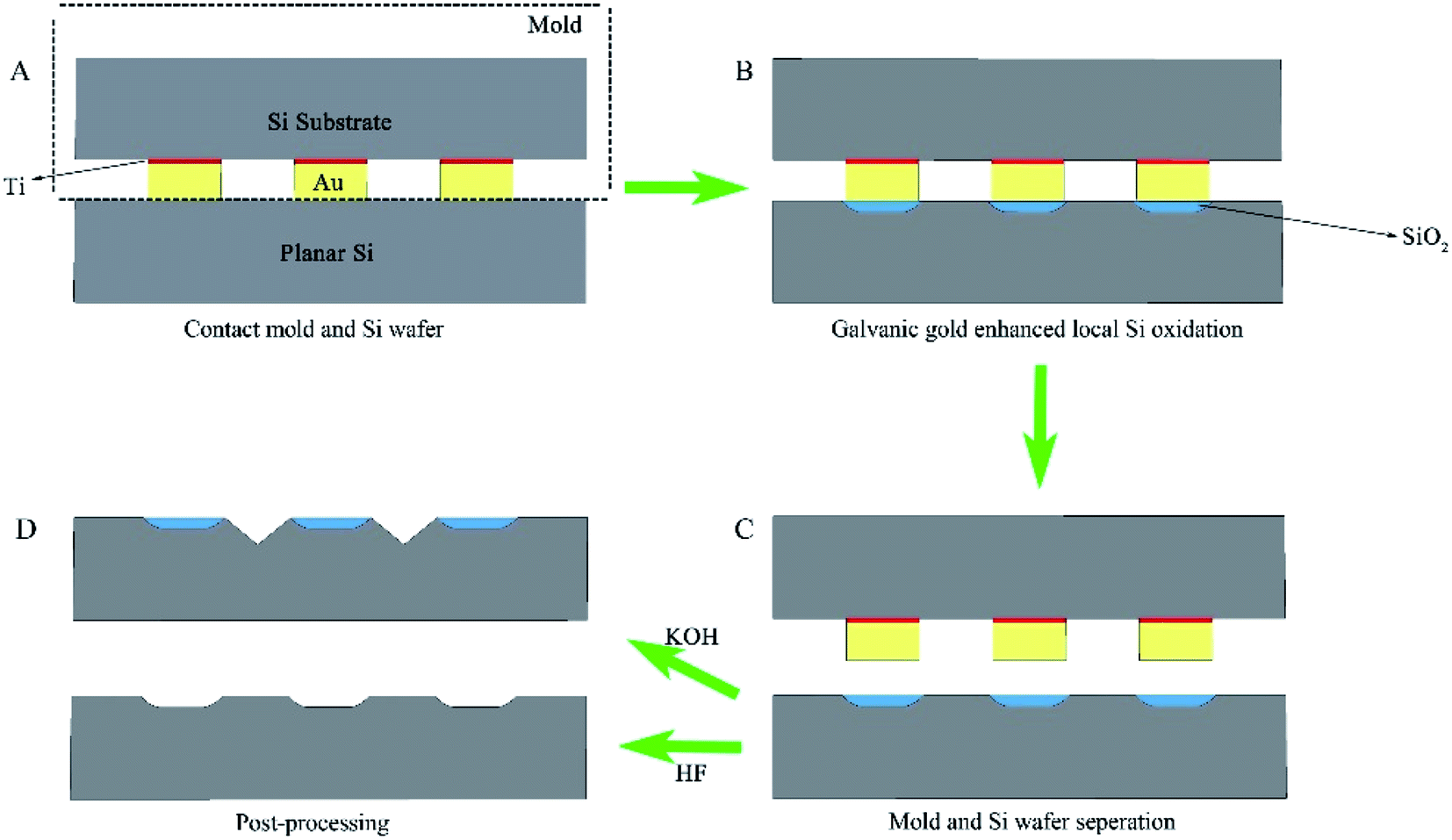 | ||
| Fig. 2 Schematic of the conceptual diagram of GMIL processing flow, showing the experimental steps involved in surface patterning on silicon wafer surface. (A) A gold mold with defined pattern is brought into close contact with the silicon wafer surface by the pressure. (B) The spontaneous generation of thin SiO2 layer pattern by gold galvanic induced site-specific silicon oxidation. (C) The gold mold and silicon wafer are separated after desired close contact time, leaving a galvanic-induced SiO2 pattern in silicon wafer surface. (D) Schematic of the processing flow in which the GMIL induced silicon oxide pattern can be selectively removed in dilute HF solution or serve as a robust etchant resist in alkaline solution, enabling the formation of regular silicon microstructures on silicon wafer surface. | ||
The surface patterning capabilities of proposed GMIL technique on silicon surface are revealed by simple wet chemical etching of GMIL–silicon in aqueous HF or KOH solutions. After etching, the as-prepared patterned silicon microstructures were examined by using a high-resolution field-emission scanning electron microscope (SEM). We found that the pattern of the gold mold can be transferred onto the silicon wafer surface with high fidelity, and large-area arrays of various patterned silicon microstructures can be achieved after simple wet chemical etching. Shown in Fig. 3 are the top-view SEM images of the gold molds, and the corresponding silicon patterns after 10 min wet etching in aqueous HF solution. The photogram images of the used gold pillar and grating molds are shown in Fig. S2.† Large-area periodic shallow pits and gratings arrays in silicon surface (p-Si, B doped, 1–10 Ω cm) are achieved after etching in dilute HF solution, indicating the removal of SiO2 galvanic generated in silicon/gold interface. The SEM images show that the resulting shallow Si pits (Fig. 3B) and trenches (Fig. 3D) after etching in aqueous HF solution are consistent with the gold master mold features (Fig. 3A and C), revealing the SiO2 removal process replicates the features from the gold master mold and that the achievable GMIL resolution increased with decreasing lateral dimensions of gold patterns. For short time contact, the diameter of the pits and width of the trenches are slightly smaller than those of the gold master molds. The size variations may come from the slight shrink of the true microcontact areas between the gold molds and silicon substrates, which was caused by the shrinking effect of the top surface of gold pillars and gratings during gold deposition by e-beam evaporation. In other words, both the resolution and quality of pattern silicon structures exclusively depend on the gold mold fabrication process. Significantly, the gold master mold after more than 10 times of GMIL usage shows no observable damage (Fig.S3†) revealing the remarkable durability of the gold mold.
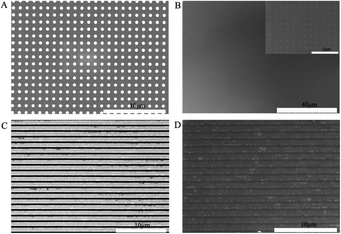 | ||
| Fig. 3 The top-view SEM images. (A) SEM image of gold mold with periodic pillars. (B) SEM of large-area periodic shallow pits produced after GMIL process using gold pillar mold and wet etching in dilute aqueous HF solution. The inset shows a magnified SEM image of the shallow pits. (C) SEM image of gold mold with periodic gratings. (D) SEM of periodic shallow trenches produced after GMIL process using gold grating mold and wet etching in dilute aqueous HF solution. | ||
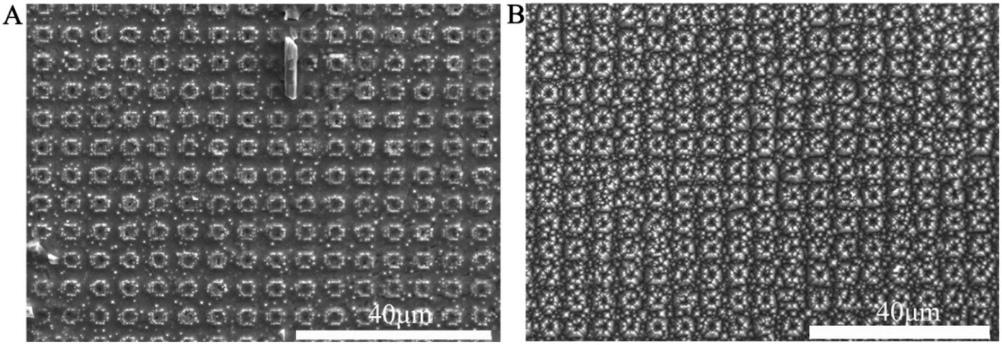
Silicon oxide layer is not attacked by aqueous alkaline solution and therefore has been widely used as “hard mask” or etchant resist for alkaline etching. To show the utility of the GMIL strategy for practical lithographic processes, we experimentally study the effect of GMIL-induced silicon oxide patterns acting as robust etchant resist in alkaline solutions (a mixed 5% KOH and 8% isopropanol aqueous solution was used due to its well-controlled behavior). Fig. 4 shows the SEM images of the typical periodic arrays of upright pyramid and inverted pyramid formed with galvanic induced thin SiO2 layer on p-Si wafer surface as robust etchant resists by GMIL with different gold master molds. Some defects in these micro pyramid arrays are induced by the imperfect gold mold, but the overall periodic pyramidal structures are comparable to those prepared through conventional photolithography methods and alkaline etching. Both pyramid and inverted pyramid arrays are well known to be excellent light trapping structures for silicon solar cells. The upright and truncated pyramids are manufactured by using the gold pillar mold for GMIL and then wet KOH etching, while the inverted pyramids are manufactured by using the gold hole mold for GMIL and then wet KOH etching. Fig. S4† shows the cross-sectional SEM images of upright and inverted silicon pyramids by GMIL process. The successful fabrication of periodic pyramids and inverted pyramids indicates that the spontaneously GMIL-patterned thin SiO2 layer can effectively act as robust etchant resists for chemical texturing the underlying silicon with the use of simple wet alkaline etching. The size and arrangement of the pyramids are defined by the GMIL-patterned thin SiO2 resists, which can be programmed through gold mold design, implying that GMIL technique provides a simple and versatile tool for surface patterning on silicon wafer surfaces.
 | ||
| Fig. 4 SEM images of the typical periodic upright pyramid and inverted pyramids on silicon surface formed with galvanic induced thin SiO2 layer as robust etchant resists in aqueous KOH solutions. (A, B) Low- and high magnification SEM image of periodic silicon pyramids. (C) SEM image of truncated silicon pyramid. (D) SEM image of inverted silicon pyramid. | ||
Fig. 5 further shows the SEM images of patterned silicon surfaces manufactured by using the large-sized pillar gold mold for GMIL and wet KOH etching with and without isopropyl alcohol. It can be clearly seen that these GMIL microstructures are rather complex compared with those manufactured with nanometer-sized pillar gold mold, indicating the large-sized pillar molds greatly hold back the galvanic induced silicon oxidation process under the whole area of contact due to the close contact between mold and silicon surface, which seriously prevent the reactive diffusion of oxygen and water into the silicon/gold interface.
 | ||
| Fig. 5 SEM images of patterned silicon surfaces with complex structures through GMIL and wet KOH etching. (A) 5 min 5% KOH solution etching. (B) 3.5 min mixed 5% KOH and 8% isopropanol solution etching. | ||
4. Conclusion
In conclusion, our experiments successfully show the simple straightforward surface patterning capabilities of the GMIL technique on silicon wafers. The achievable GMIL geometry and the quality depended on the noble metal master mold patterns. Although the current GMIL technique may not yet match the conventional lithographic methods due to challenges such as the fabrication of high-quality gold molds, it nevertheless offers many unprecedented opportunities for the easy and cheap realization of surface patterning. Provided further optimization of this method especially molds fabrication, GMIL can be of great interest as easily accessible, simple and low-cost alternative lithography strategy for generating surface patterns on silicon wafer surfaces with no requirement of expensive and sophisticated instrumentation and facilities.Conflicts of interest
There are no conflicts to declare.Acknowledgements
We acknowledge financial support from National Natural Science Foundation of China (51972031) and Natural Science Foundation of Beijing Municipal (2172030). F. Q. Z. and H. X. F. performed all the experiments and data analysis. K. Q. P. conceived the experiments, analyzed the data and wrote the manuscript.References
- B. D. Gates, Q. B. Xu, M. Stewart, D. Ryan, C. G. Willson and G. M. Whitesides, Chem. Rev., 2005, 105, 1171–1196 CrossRef CAS.
- L. J. Guo, Adv. Mater., 2007, 19, 495–513 CrossRef CAS.
- S. Y. Chou, C. Keimel and J. Gu, Nature, 2002, 417, 835–837 CrossRef CAS PubMed.
- F. W. Huo, Z. J. Zheng, G. F. Zheng, L. R. Giam, H. Zhang and C. A. Mirkin, Science, 2008, 321, 1658–1660 CrossRef CAS PubMed.
- S. Y. Chou, P. R. Krauss and P. J. Renstrom, Science, 1996, 272, 85–87 CrossRef CAS.
- W. Shim, A. B. Braunschweig, X. Liao, J. N. Chai, J. K. Lim, G. F. Zheng and C. A. Mirkin, Nature, 2011, 469, 516–520 CrossRef CAS PubMed.
- D. Pires, J. L. Hedrick, A. De Silva, J. Frommer, B. Gotsmann, H. Wolf, M. Despont, U. Duerig and A. W. Knoll, Science, 2010, 328, 732–735 CrossRef CAS PubMed.
- W. S. Liao, S. Cheunkar, H. H. Cao, H. R. Bednar, P. S. Weiss and A. M. Andrews, Science, 2012, 337, 1517–1521 CrossRef CAS PubMed.
- R. Garcia, A. W. Knoll and E. Riedo, Nat. Nanotechnol., 2014, 9, 577–587 CrossRef CAS.
- S. F. Lyuksyutov, R. A. Vaia, P. B. Paramonov, R. M. Ralich, G. Sigalov and E. Sancaktar, Nat. Mater., 2003, 2, 468–472 CrossRef CAS PubMed.
- R. B. Comizzoli, R. P. Frankenthal, P. C. Milner and J. D. Sinclair, Science, 1986, 234, 340–345 CrossRef CAS PubMed.
- X. G. Zhang, Galvanic Corrosion, in Uhlig's Corrosion Handbook, John Wiley and Sons Inc., 2011, pp. 123–143 Search PubMed.
- Y. Sun and Y. Xia, Science, 2002, 298, 2176–2179 CrossRef CAS PubMed.
- E. González, J. Arbiol and V. F. Puntes, Science, 2011, 334, 1377–1380 CrossRef PubMed.
- M. H. Oh, T. Yu, S. H. Yu, B. K. Lim, T. Ko, M. G. Willinger, D. H. Seo, B. H. Kim, M. G. Cho, J. H. Park, K. Kang, Y. E. Sung, N. Pinna and T. Hyeon, Science, 2013, 340, 964–968 CrossRef CAS PubMed.
- J. E. Macdonald, M. B. Sadan, L. Houben, I. Popov and U. Banin, Nat. Mater., 2010, 9, 810–815 CrossRef CAS.
- S. E. Skrabalak, J. Y. Chen, Y. G. Sun, X. M. Lu, L. Au, C. M. Cobley and Y. N. Xia, Acc. Chem. Res., 2008, 41, 1587–1595 CrossRef CAS.
- H. Morinaga, M. Suyama and T. Ohmi, J. Electrochem. Soc., 1994, 141, 2834–2841 CrossRef CAS.
- H. Morinaga, T. Futatsuki, T. Ohmi, E. Fuchita, M. Oda and C. Hayashi, J. Electrochem. Soc., 1995, 142, 966–970 CrossRef CAS.
- X. Li and P. W. Bohn, Appl. Phys. Lett., 2000, 77, 2572–2574 CrossRef CAS.
- K. Q. Peng, Y. J. Yan, S. P. Gao and J. Zhu, Adv. Mater., 2002, 14, 1164–1167 CrossRef CAS.
- K. Q. Peng, Y. Wu, H. Fang, X. Y. Zhong, Y. Xu and J. Zhu, Angew. Chem., Int. Ed., 2005, 44, 2737–2742 CrossRef CAS PubMed.
- K. Q. Peng and S. T. Lee, Adv. Mater., 2011, 23, 198–215 CrossRef CAS PubMed.
- K. Q. Peng, J. J. Hu, Y. J. Yan, Y. Wu, H. Fang, Y. Xu, S. T. Lee and J. Zhu, Adv. Funct. Mater., 2006, 16, 387–394 CrossRef CAS.
- K. Q. Peng, A. J. Lu, R. Q. Zhang and S. T. Lee, Adv. Funct. Mater., 2008, 18, 3026–3035 CrossRef CAS.
- A. I. Hochbaum, R. K. Chen, R. D. Delgado, W. J. Liang, E. C. Garnett, M. A. Najarian and P. D. Yang, Nature, 2008, 451, 163–167 CrossRef CAS PubMed.
- K. Q. Peng, Y. Xu, Y. Wu, Y. J. Yan, S. T. Lee and J. Zhu, Small, 2005, 1, 1062–1067 CrossRef CAS PubMed.
- C. Huo, J. Wang, H. Fu, X. Li, Y. Yang, H. Wang, A. Mateen, G. Farid and K. Q. Peng, Adv. Funct. Mater., 2020, 30, 2005744 CrossRef CAS.
- K. Q. Peng, X. Wang, L. Li, Y. Hu and S. T. Lee, Nano Today, 2013, 8, 75–97 CrossRef CAS.
- S. W. Chang, J. Oh, S. T. Boles and C. V. Thompson, Appl. Phys. Lett., 2010, 96, 153108 CrossRef.
- K. Q. Peng, X. Wang, L. Li, X. L. Wu and S. T. Lee, J. Am. Chem. Soc., 2010, 132, 6872–6873 CrossRef CAS PubMed.
- K. S. Brammer, C. Choi, S. Oh, C. J. Cobb, L. S. Connelly, M. Loya, S. D. Kong and S. Jin, Nano Lett., 2009, 9, 3570–3574 CrossRef CAS PubMed.
- W. Chern, K. Hsu, I. S. Chun, B. P. de Azeredo, N. Ahmed, K. H. Kim, J. Zuo, N. Fang, P. Ferreira and X. Li, Nano Lett., 2010, 10, 1582–1588 CrossRef CAS PubMed.
- J. Wang, Y. Hu, H. Zhao, H. Fu, Y. Wang, C. Huo and K. Q. Peng, Adv. Mater. Interfaces, 2018, 5, 1801132 CrossRef.
- J. Weisse, D. Kim, C. Lee and X. Zheng, Nano Lett., 2011, 11, 1300–1305 CrossRef CAS PubMed.
- Y. Hu, K. Q. Peng, Z. Qiao, X. Huang, F. Q. Zhang, R. N. Sun, X. M. Meng and S. T. Lee, Nano Lett., 2014, 14, 4212–4219 CrossRef CAS PubMed.
- B. P. Azeredo, Y. W. Lin, A. Avagyan, M. Sivaguru, K. Hsu and P. Ferreira, Adv. Funct. Mater., 2016, 26, 2929–2939 CrossRef CAS.
- K. Q. Peng, M. L. Zhang, A. J. Lu, N. B. Wong, R. Q. Zhang and S. T. Lee, Appl. Phys. Lett., 2007, 90, 163123 CrossRef.
- K. Q. Peng, M. L. Zhang, A. J. Lu, N. B. Wong, R. Q. Zhang and S. T. Lee, Appl. Phys. Lett., 2007, 90, 163123 CrossRef.
- W. K. Choi, T. H. Liew, M. K. Dawood, H. I. Smith, C. V. Thompson and M. H. Hong, Nano Lett., 2008, 8, 3799–3802 CrossRef CAS.
Footnote |
| † Electronic supplementary information (ESI) available. See DOI: 10.1039/d1ra02459k |
| This journal is © The Royal Society of Chemistry 2021 |