
 Open Access Article
 This Open Access Article is licensed under a Creative Commons Attribution-Non Commercial 3.0 Unported Licence
Enhanced reliability of phase-change memory via modulation of local structure and chemical bonding by incorporating carbon in Ge2Sb2Te5†
Jeong Hwa Han‡
a,
Hun Jeong‡a,
Hanjin Park‡b,
Hoedon Kwona,
Dasol Kima,
Donghyeok Limc,
Seung Jae Baikd,
Young-Kyun Kwon *be and
Mann-Ho Cho*af
*be and
Mann-Ho Cho*af
aDepartment of Physics, Yonsei University, Seoul, 03722, Republic of Korea. E-mail: mh.cho@yonsei.ac.kr
bDepartment of Physics, Research Institute for Basic Sciences, Kyung Hee University, Seoul, 02447, Republic of Korea. E-mail: ykkwon@khu.ac.kr
cDepartment of Materials Science and Engineering, UNIST, Ulsan, 44919, Republic of Korea
dFaculty of Electronic and Electrical Engineering, Hankyong National University, Anseong, 17579, Republic of Korea
eDepartment of Information Display, Kyung Hee University, Seoul, 02447, Republic of Korea
fDepartment of System Semiconductor Engineering, Yonsei University, Seoul, 03722, Republic of Korea
First published on 25th June 2021
Abstract
In this study, we investigated the effect of phase-change characteristics on the device performance of carbon-incorporated Ge2Sb2Te5 (CGST) to understand the origin of the enhanced reliability and stabilization of the device. Macroscopic and microscopic measurements confirmed that the structural stability significantly increased with the incorporation of as much as 10% carbon. After the completion of bond formation between C and Ge, the excess C (>5 atomic%) engages in bonding with Sb in localized regions because of the difference in formation energy. These bonds of C with Ge and Sb induce non-uniform local charge density of the short-range order. Finally, because the strong bonds between Ge and C shorten the short Ge–Te bonds, the high thermal stability of CGST relative to that of GST can be attributed to intensified Peierls distortion. The formation of strong bonds successfully underpins the local structures and reduces the stochastic effect. Moreover, extension of the C bonding to Sb enhances the structural reliability, resulting in highly stable CGST in the amorphous phase. Finally, the device stability of CGST in the reset state of the amorphous structure during the device switching process was significantly improved.
Introduction
Owing to its many advantages, such as high speed, low power consumption, good endurance, and excellent scaling ability, phase-change random access memory (PRAM) has been successfully developed for commercialization.1–3 However, the performance of PRAM has not yet surpassed the excellent operating speed of dynamic random access memory (DRAM) and the high degree of integration of NAND flash memory. More specifically, the switching speed needs to be improved to be comparable to that of DRAM, and its process technology needs to be refined to achieve a high integration density similar to that of NAND flash memory.4 To solve these problems, the development of a suitable system consisting of a doped material that offers low energy consumption and a super-lattice structure that enables high operating speed has been targeted by many researchers. The key factors required for phase-change operation are closely related to the atomic-level microstructures, such as Peierls distortion and metal bonding,5,6 which affect each other and are systemically connected. By generating the Peierls distortion, the periodic grid distortion of the crystal is increased, and electron delocalization for metal bonding is simultaneously induced. Recent studies have reported significant improvements in switching characteristics, such as the switching speed, phase transition temperature, and thermal stability, through the modulation of Peierls-like distortions, as well as the bonding characteristics of Sb2Te3. That is, the change in the local structure and bonding characteristics between neighboring atoms around the metal dopants, such as Ti7,8 and Sc,9 affect the phase-change characteristics. Despite improvements in the phase-change performance, the data suggest that improvements in the thermal stability of the Sb2Te3-based phase change are insufficient.The thermal stability of GST is a critical issue for reliable device operation. Several studies on the switching characteristics of GST using various metallic10–12 and nonmetallic element dopants,13–16 such as Al, Ag, N, and C, have been reported. With regard to covalent nitrogen doping into Ge–Sb–Te (GST), variations in the electronic structure and chemical bonding13 characteristics critically affect the thermal stability and phase-change process of GST. Verification using the data for carbon content of less than 10%, as reported by Tao Li et al.,16 for the local structure was not performed, and only limited structural stability without any device reliability was demonstrated. In another case of highly C-doped GST (CGST > ∼18%), C–C chains significantly altered the amorphous structure by disordering the Ge–Te tetrahedral network.14–16 Therefore, the fraction of the tetrahedral local structure can be successfully increased, resulting in an increase in electrical resistance and a hindrance in electrical switching capability.17 However, the dependence of the device characteristics on the programming pulse showed that the crystallization switching speed and resistance ratio were significantly degraded when the C content exceeded 10%, while the reset power and structural stability of CGST were enhanced by the notable change in thermal conductivity.
In this study, we focused on the change in the atomic level of the microscopic structures of C-doped GST for which the atomic C content is ∼10%, because the device characteristics, including the thermal stability for C content less than ∼10%, have not been sufficiently considered. That is, although the phase-change characteristics changed rapidly (depending on the amount of dopant) as a result of the inherent Peierls distortion and metavalent bonding properties of the phase-change material, the effect of the local structure on the device performance, resulting from the incorporation of C, and the phase-change characteristics when the C content does not exceed ∼10% has not yet been fully investigated. The results of the optimized local structures using molecular dynamics calculations18 and extended X-ray absorption fine structure (EXAFS)19,20 examination revealed that a change in the localized charge density can be induced by modulation of the bond length between Ge and Te because of the formation of Ge–C and Sb–C bonds, regardless of the C–C chains. In particular, for a low amount of incorporated carbon (less than ∼5 atomic%), non-uniform charge density was induced near the Ge–C bonds, and the bond length between Ge and Te was slightly shorter than that in GST. In contrast, when the amount of incorporated carbon was higher than 5 atomic% and close to 10 atomic%, the non-uniform charge density induced near the Ge–C bond was relaxed because a new bond between Sb and C was generated. The dependence of these changes in the bonding characteristics on the quantity of carbon affects the overall charge density and distribution of the local structures. Finally, in amorphous GST, carbon predominantly coordinates to form complexes with tetrahedral and pyramidal structures. Therefore, the predominant formation of complexes in amorphous structures critically increases the crystallization temperature and stability in the amorphous phase by interfering with crystallization. This improves the phase-change performance of devices in the form of increased endurance, decreased resistance drift,21,22 and increased electrical field difference (ΔV) between the set and reset states.
Results and discussion
Change in the phase transition temperature with C content
In general, the formation of a defective-octahedral structure in crystalline GST results from the energetic stability resulting from Peierls distortion, which results in different Ge–Te bond lengths, including three short and three long bonds.19,20 Thus, it is important to determine the relationship between the transition behavior and the modulation in structural distortion owing to C. To investigate the crystalline structure of C-doped GST films, we used the X-ray diffraction (XRD) technique to measure the diffraction angle as a function of the annealing temperature. Fig. 1(a)–(c) show the structural evolutions from the as-grown amorphous to the crystalline structures in the pristine and carbon-doped GST films (5% and 10%, respectively) as a function of the annealing temperature. The change in the diffraction angles of the peaks of GST clearly shows two transition processes: one transition from the amorphous to the fcc structure (Tcry1: amorphous to fcc phase) is generated below the annealing temperature of 200 °C and the other transition from the fcc to the hexagonal close-packed (hcp) structure (Tcry2: fcc to hcp phase) occurs at annealing temperatures of 300 °C and 350 °C (Fig. 1(a)). In CGST (∼5%), the transition temperatures, Tcry1 and Tcry2, increase to Tcry1 = ∼250 °C and Tcry2 > ∼450 °C, respectively (Fig. 1(b)). When the C content was increased to 10% (CGST(10%)), Tcry1 remained nearly the same or increased slightly (Tcry1 ≥ ∼250 °C), whereas Tcry2 was not clearly observed even at an annealing temperature of 500 °C (Fig. 1(c)). We found the peak positions for the fcc structures (in the green-shaded regions in the figures) in the CGST(5%) and CGST(10%) films to be nearly the same as those of the pristine GST film, which is consistent with those of the reported GST film.23 More specifically, the absence of peak shift indicates that the lattice parameters of the fcc crystalline structure do not change with the incorporation of C. It is interesting to note that the stabilities of the amorphous and fcc crystal structures were significantly improved, although the accompanying structural distortions were not observed significantly. This is because, in the well-known phase transition process of GST from amorphous to fcc structures, the stability of each structure critically affects the device reliability.24–26 Despite the incorporation of the C dopant into the film, XRD did not enable us to clearly observe any distortion in the structure; rather, the dopant improved the energetic stability of the fcc crystalline structure. In particular, the fcc structure of CGST(10%) with a high C concentration was retained even at an annealing temperature of 500 °C, whereas pure GST transformed to the hcp structure at 350 °C. This implies that the incorporation of carbon, which ameliorates the structural stability of both the amorphous and fcc phases, enhances the bond strength in GST films. The increase in the phase transition temperatures from the amorphous to the fcc and from the fcc to the hcp phases may be highly advantageous for device operation. The tolerance to the applied power and stability in the set state can be improved by increasing the crystallization temperature for the fcc phase, compared with GST. The formation of the hexagonal phase, which is always accompanied by severe volume shrinkage, results in the subsequent generation of large voids, likely causing device failure. In addition, the suppression of this phase is also expected to be advantageous for device performance, such as promoting the endurance and retention characteristics.4,23,27 | ||
| Fig. 1 (a)–(c) X-ray diffraction data: θ–2θ scans of (a) crystalline GST, (b) CGST(5%), and (c) CGST(10%) films. The blue, green, and red areas indicate the amorphous (as-grown), fcc crystalline, and fcc + hcp crystalline states, respectively. The peak positions of the CGST films are nearly the same as those of the GST film, indicating that the lattice parameters of the crystalline structure do not change with the incorporation of C. (d)–(f) Plots of sheet resistance as functions of annealing temperature for the (d) GST, (e) CGST(5%), and (f) CGST(10%) films. Tc of CGST is higher than that of GST. | ||
The temperature-dependent resistance change was measured to confirm the stability of the phase-change properties, such as the resistance modulation and crystallization temperature, using a simple device structure, as shown in Fig. 1(d)–(f). In all samples, the resistance change caused by the structural phase transition was also clearly observed, that is, the resistance significantly changed from ∼107 Ω in the amorphous structure to ∼103 Ω in the crystalline structure. Moreover, it was observed that the higher C content in GST yields a higher Tcry, but without noticeable changes in the resistance values of their corresponding fcc crystalline phases. The changes in Tcry1 (∼150 °C) and Tcry2 (∼300 °C) of the GST film, as shown in Fig. 1(d)–(f), agree well with the values reported for GST films.13,21,23 In the CGST films, the crystallization process occurred at temperatures higher than those of the GST films. Specifically, Tcry1 and Tcry2 observed for the CGST(5%) film were ∼180 and ∼380 °C, respectively. The fact that the CGST films transformed from the amorphous to the fcc and hcp phases at higher transition temperatures than the pristine GST film indicates that the incorporated carbon atoms play a blocking role in the phase transition process, thereby requiring higher activation energy27 for crystallization. For the CGST film with 10% C concentration, Tcry1 increased slightly over ∼190 °C, but Tcry2 could not be determined even above 400 °C. Fig. 1(f) shows the change in resistance with temperature, indicating that the film did not undergo a phase transition to the metallic hcp phase; instead, the fcc structure was retained with semiconducting characteristics up to an annealing temperature of 400 °C. We emphasize that the slope change in resistance over ∼340 °C was not caused by the formation of the metallic hcp phase but by the expansion of the fcc crystalline domains, which is consistent with the XRD data, implying that a higher C concentration would suppress the 2nd phase transition from the semiconducting fcc to the metallic hcp phase. To systematically understand the effects of the carbon concentration and the effect of adding carbon as a dopant on the 1st and 2nd phase transitions, we investigated the extent to which the chemical bonds depended on the modulation in the local environment owing to the incorporation of carbon in both the 5% and 10% CGST films.
Change in local structure with C content
Raman spectroscopy was employed to investigate the modulation of the phonon characteristics resulting from the change in the local environment as a result of the incorporated carbon, as shown in Fig. 2. As expected from the XRD data presented above, which did not indicate a critical change in the structure of CGST, no peaks evidential of the generation of a new structure were found. Instead, only the phonon vibrations28 of the CGST films were observed to undergo mode shape changes. Fig. 2(a)–(c) clearly show that the Raman spectra of the amorphous structure comprise five sub-peaks, regardless of the C content.15,29–31 The spectra of the films that were re-amorphized by laser irradiation31 after the first crystallization are similar to those of the amorphous structure of the as-grown films. All the spectra also comprise five sub-peaks, as shown in Fig. 2(d)–(f). The A peak located at 80 cm−1 represents the E mode of the bending vibrational GeTe4 tetrahedron, whereas the B peak at 102 cm−1 is ascribed to the defective octahedron of Ge.15,29–31 Another peak at 125 cm−1 (C peak) is attributed to the A1 mode of the GeTe(4−n)Gen (n = 1, 2, eventually 0) corner-sharing tetrahedral structure and is based on the assignment for the amorphous GeTe layer and lighter Ge2Te3 complexes.15,28–30 The main peak (D peak) at 165 cm−1 is the result of the Sb–Te bond vibrations of the defective-octahedral units in Sb2Te3.15,29–31 In addition, the weak broad peak (E peak) observed at 220 cm−1 can be attributed to the F2 mode of the rhombohedral deformed rock-salt structure and bending modes of the GeTe4 tetrahedral structure.15,29–31 Although all CGST amorphous films exhibited similar Raman spectra in terms of the peak positions, changes in the two local environments of the tetrahedral structure (A, C, and E peaks) and defective-octahedral structure (B and D peaks) clearly reveal a tendency of dependence on the incorporated C content, as shown in ESI Table S1.† Because the vibrational modes of the amorphous (tetrahedral and pyramidal) and crystalline (octahedral and defective-octahedral) structures are distinct,24 the sums of the peak areas of these two distinct structures in the as-grown film could be compared with those in the re-amorphized film. To easily compare the relative portion of the amorphous phase in the as-grown film with that of the re-amorphized film, the summation of the peak area for the amorphous phase (A + C + E) was divided by that of the crystalline phase (B + D) using the values in ESI Table S1,† and the results are provided in Table 1. The data show that the proportion of amorphous structure in the re-amorphized film increases with the amount of carbon. We also observed that the portion of the amorphous structure in CGST(10%) was significantly enhanced compared to that in CGST(5%). This suggests that C affects the local order of GST in the amorphous phase by elevating the fraction of tetrahedral Ge atoms, resulting in an improvement in the thermal stability of the amorphous phase. | ||
| Fig. 2 Variation in the nonpolarized Raman spectra of the (a)–(c) amorphous and (d)–(f) re-amorphized GST, CGST(5%), and CGST(10%) films, respectively. The spectra were deconvoluted into five vibration modes, denoted by A to E in the figure. | ||
| Peak area ratioa | Samples | |||||
|---|---|---|---|---|---|---|
| Amorphous GST | Re-amorphized GST | Amorphous CGST(5%) | Re-amorphized CGST(5%) | Amorphous CGST(10%) | Re-amorphized CGST(10%) | |
| a Calculations were based on the vibration peaks corresponding to the amorphous (tetrahedral and pyramidal) and crystalline (octahedral and defective-octahedral) structures in Table S1. | ||||||
| (A + C + E)/(B + D) | 0.6047 | 0.5184 | 0.6043 | 0.6235 | 0.7916 | 1.0164 |
Furthermore, to confirm the chemical bonding state resulting from changes in the local environment of CGST, X-ray photoelectron spectroscopy (XPS) with an in situ measurement system was used to exclude oxidation effects. Using the reported XPS core-level spectra of Ge 3d in octahedral and defective-octahedral structures (Geoct+def-oct), 29.6–29.7 eV, and in the tetrahedral and pyramid structures (Getet+pyr), 30.0–30.1 eV, we examined the differences in the bonding energies of the different crystalline structures, as shown in ESI Fig. S1.†24,26 As the quantity of incorporated carbon increases, the peak of Geoct+def-oct decreases, whereas the peak of Getet+pyr increases in all phases of the amorphous and crystalline structures. This suggests that the doped C atoms affect the local order of amorphous GST by increasing the fraction of tetrahedral Ge atoms. The ratio of the Ge 3d peak of the amorphous (tetrahedral and pyramidal structures) to the crystalline structure (octahedral and defective-octahedral structures), (Getet+pyr)/(Geoct+def-oct) was evaluated as a function of the carbon concentration for the three different phases, as shown in Fig. S2.† The value clearly shows that the peak area of (Getet+pyr) in the amorphous state increases with the quantity of incorporated carbon in GST, which is consistent with the Raman data. The decrease in the crystallized portion of CGST indicates that crystallization from the amorphous to the fcc structure and from the fcc to the hcp structure can be effectively hindered in CGST, compared with GST. We also confirmed that the intensity of the peaks of the chemical states of the Ge–C or Sb–C bonds is dependent on the amount of C content.33 The Sb–C bonds were observed only at a C concentration of 10% with a binding energy of ∼34 eV, suggesting that the Sb–C bonds could be closely related to the differences in the structures, thereby resulting in resistivity changes in samples with a high C concentration. This indicates that the formation of Sb–C bonding may hinder the crystallization more effectively.
To obtain information on the local structure, such as atomic distances and coordination numbers, we performed EXAFS measurements for the Ge K-edge. The fitted data based on the optimized structure are presented in the R-space in Fig. 3(a)–(c) as a function of the quantity of carbon incorporated in the GST. Using the fitted Ge K-edge spectra, we obtained direct insight into the minute structural changes in the crystalline phase (fcc phase) with the quantity of incorporated carbon. The data clearly show that six Ge–Te bonds are composed of three short and three long bonds in the crystalline GST films owing to the Peierls distortion.19,20 In addition, the Ge–Te short bond lengths of GST, CGST(5%), and CGST(10%) were determined to be 2.83, 2.76, and 2.81 Å, respectively, as shown in Table S2.† Remarkably, the short bonds in the CGST(5%) became shorter than those of GST as a result of the incorporated carbon, whereas the long bond became relatively longer than that of pristine GST. However, for a high percentage of incorporated carbon (CGST(10%)), the short bonds were considerably relaxed such that the bond length was nearly the same as that of the Ge–Te short bonds in GST. The modulation in the local structures resulting from the incorporated carbon was more closely investigated by evaluating the bond angle distributions of various constituent atoms, as shown in Fig. 3(d)–(f) and S3.† The bond angle distribution of Te–Ge–X (X = C, Ge, Sb, or Te) became broader as the carbon concentration increased, as shown in Fig. 3(d). Our detailed analysis revealed that the relatively broad shoulder peak at approximately 60° observed in CGST(5%) mainly originated from the second nearest neighbor atoms located near the cutoff distance, whereas the shoulder at approximately 60° in CGST(10%) was furnished primarily by the pyramidal configurations. Furthermore, because the carbon in CGST(10%) significantly affects the Ge-centered local structures, the change in the local structure partially generates tetrahedral bonding configurations, resulting in a shoulder peak near 109.5°. An even more intriguing feature was observed in the angular distributions of the Sb-centered or Te–Sb–X bonds depicted in Fig. 3(e): only CGST(10%) exhibits a relatively large distribution centered at 109.5°, which is not observed in other cases, and which originates from the tetrahedral Te–Sb–C bonds. This is further verified by the results in Fig. 3(f), which represent the angle distribution functions of the C-centered bonds Ge–C–X and Sb–C–X. The distributions of the Ge–C–X bonds are observed for both CGST(5%) and CGST(10%), whereas those of the Sb–C–X bonds are only observable for CGST(10%). The distribution also indicates that C-centered bonds prefer tetrahedral bonding. The data additionally support that, in CGST(5%), the structural distortion is strengthened by the C–Ge bonds, whereas in CGST(10%), the structural relaxation is caused by C–Sb bonding. The radial distribution function g(r) also supports the change in the Ge–Te and Sb–Te bonds as well as the evolution of chemical bonds with C, as shown in Fig. S4.† The calculated data are consistent with the obtained XPS and EXAFS data: when the quantity of incorporated C is larger than 5%, the generation of C–Sb bonds significantly affects the radial distribution and the difference between the length of long and short Ge–Te bonds.32
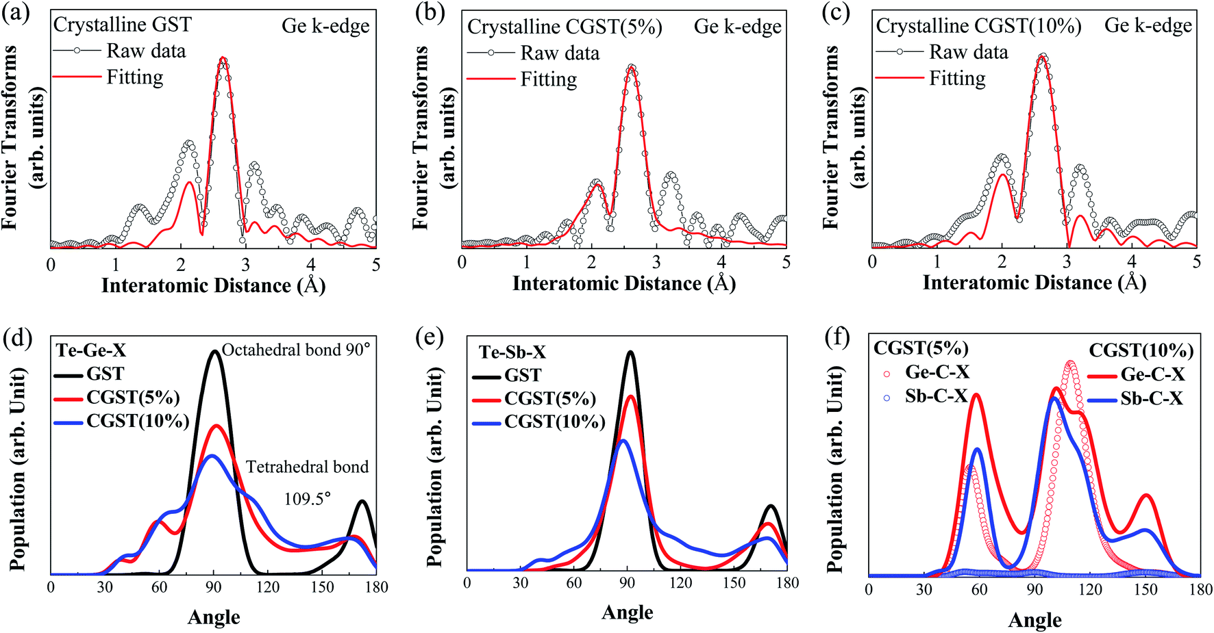 | ||
| Fig. 3 (a)–(c) Fourier-filtered Ge K-edge EXAFS data (dotted line) and fitting results (red solid line) for the (a) GST, (b) CGST(5%), and (c) CGST(10%) films. (d)–(f) Angular distribution functions used to investigate the modulation of the bonding angle of the atoms resulting from the change in the chemical bond of the incorporated carbon for (d) Ge-centered, (e) Sb-centered, and (f) C-centered bonds. | ||
Additionally, to investigate the relationship between the significant change in chemical bonding and the modulation in structural distortion due to the incorporated carbon in detail, the charge density differences (CDDs) were extracted from our DFT calculations. The CDDs show that the chemical bonding characteristics are strongly related to the structural distortions, as shown in Fig. 4(a)–(d), which display the CDDs on the cross-sectional planes of both of the optimized CGST(5%) and CGST(10%) structures. Interestingly, in the 5% CGST structure, the incorporated C participates only in the formation of Ge–C bonds, whereas in CGST(10%), C forms both Ge–C and Sb–C bonds. Thus, the distribution data show that at C concentrations lower than 5%, the nearest-neighbor charge density between Ge and Te becomes much weaker. At the atomic level, the incorporated C induces one strong bond with the nearest Ge, thereby weakening the Ge–Te bonds. Therefore, the change in the charge density modulates the bond length between Ge and Te; specifically, the short Ge–Te bond becomes shorter, whereas the long bond becomes relatively longer. Because C forms bonds with both Ge and Sb at concentrations higher than 5%, the nearest-neighbor charge density between Ge and Te becomes weaker than that of CGST(5%). The local structure of the Sb–C bond and the CDD around it show that they have the effect of enhancing the stability of the amorphous structures by increasing the structural relaxation. Thus, even by increasing the amount of carbon in GST to as much as 10%, more stable driving is possible in the phase-change operation characteristics. A detailed analysis of the changes in the charge density and bond length with increasing C content suggests that the amorphous structure is significantly stable, indicating that the use of carbon as the dopant can modulate the stochastic effect.33–36
 | ||
| Fig. 4 Device characteristics for the set and reset conditions: (a) set/reset voltages of 1.0 V/1.8 V for GST and 1.4 V/2.6 V for CGST under various pulse width conditions. (b) Set/reset voltage characteristics at a specific set/reset pulse time of 250 ns/60 ns for the most stable and shortest operation, respectively. (c) Endurance data under the various pulse conditions of set/reset: 1.0 V(250 ns)/1.8 V(60 ns) for GST and 1.4 V(250 ns)/2.6 V(60 ns) for CGST (inset: schematic of PRAM device). (d) Resistance drift for GST, CGST(5%), and CGST(10%). The set and reset voltages, crystalline resistance value, ΔV, endurance, and coefficient α increased with the C concentration in GST. | ||
Device performance with C content
The effects of incorporating C into GST on the device performance were investigated by assessing the characteristics of the set/reset operation with the pulsing time, as shown in Fig. 5(a). The data show that stable operation was achieved for both the set and reset states in CGST, while the operation pulsing time in CGST increased to 30 ns in the reset process and 20 ns in the set process, compared with that in GST. Based on these characteristics, we observed clear set/reset operation characteristics at a stable operation pulsing time, reset pulse of 60 ns, and set pulse of 250 ns, as shown in Fig. 5(b). Using the appropriate pulse condition, the reset voltage in the C-doped GST was significantly increased compared with that in GST, which is consistent with the increase in thermal stability of the amorphous structure. Owing to the increased thermal stability of CGST, the voltage difference, ΔV, between the set and reset states significantly increased from ΔV ≈ 0.6 V for GST to ΔV ≈ 1.6 V for CGST. In particular, the resistance value of the reset state was almost the same as that of the initial as-grown state, which is remarkable because the resistance value of GST decreased after reset. It is well known that the structural stability of amorphous GST is thermodynamically poor compared with that of its crystalline counterpart because the nucleation centers generated during the set process are not fully removed in the reset process. Therefore, the resistance change observed in CGST after the set/reset process strongly suggests that a significant improvement in the thermal stability of the reset state of the amorphous phase would resolve the critical reliability problem of GST devices. | ||
| Fig. 5 Charge density differences (CDDs) on various cross-sectional planes including the (a) Ge–C–Ge and (c) Ge–C–Sb bonds in CGST(5%), and the (b) Ge–C–Ge and (d) Ge–C–Sb bonds in CGST(10%). The CDD in Ge–C–Sb clearly depends on the amount of C. | ||
The reliability of the switching operation was confirmed by investigating the endurance and resistance drift of CGST-based as well as GST-based devices, as shown in Fig. 5(c) and (d). Even under high-voltage operating conditions, the reliability of the CGST device was improved compared with that of GST, as shown in Fig. 5(c) of the cycling characteristics, which reflects the increase in the structural stability of the amorphous phase. Fig. 5(d) shows the characteristics of the resistance drift, which also verifies the improvement in the device stability in the reset state of the amorphous phase. Interestingly, although the operating voltage for the set/reset process between CGST(5%) and CGST(10%) did not differ, the reliability continuously improved with the quantity of C incorporated in GST. Thus, the change in reliability related to the physical characteristics owing to the incorporated carbon suggests that the stochastic effect was effectively improved as the quantity of C increased. However, as the set and reset voltages of CGST increase, the power consumption inevitably increases, as indicated in Table S3;† the reset energy for both the CGST(5%) and CGST(10%) devices was evaluated to be ∼0.2 nJ, which is slightly more than twice that of GST. We did not observe any significant increase in the reset energy for CGST(10%) compared to CGST(5%). Overall, although more energy is required for the phase-change process, the reversible electrical switching capability of the phase-change memory cells was successfully improved in terms of endurance.
In GST with a very high C content (18%), the incorporated carbon accumulated at the grain boundary hindered grain growth. The presence of stable C–C chains with strong chemical bonds produced a higher network rigidity, resulting in an extremely high thermal stability of the amorphous GSTC material with a degradation of the phase-change performance.15 Considering the roles of Ge and Sb when the amount of C in the microstructure is less than 10%, the dependence of the strengthening of the structural stability on the amount of C in the amorphous phase is likely attributable to the combined role of the C–Ge and C–Sb bonding states. That is, although the C–Ge bond in CGST(5%) and CGST(10%) increased the Peierls distortion, the bonding hindered the movement of Ge atoms in the phase-change process between the amorphous and crystalline phases. Therefore, the bonding acts to increase the phase-change energy and operating voltage in the set/reset process. Thus, the stabilization in the amorphous phase is enhanced owing to the formation of the C–Ge chemical bonds, which contribute to the improvement in the endurance characteristics of the device. In contrast, the C–Sb bonding in CGST(10%) is the factor responsible for further increasing the stability of the amorphous phase by mitigating the distortion caused by the C–Ge bonding. Therefore, although the operating voltage hardly changes, it is possible to further improve the endurance performance. Finally, based on the consistent device performance with the microstructural modulation resulting from the incorporated C, the phase-change operation for the reset process, including the critical problem caused by the stability of the amorphous phase, can be successfully improved by controlling both the roles of Ge and Sb.
Conclusions
A rapid and energy-efficient phase change was achieved based on the bonding properties resulting from unique structural characteristics, such as the Peierls distortion. These two core performance indicators for the phase-change characteristics conflict with the mutual properties; therefore, a more specific structural change is required to improve both. In Sb2Te3 systems with fast phase-change properties, material stability under conditions that do not adversely affect this property is desirable. Ti and Sc dopants can be used for this purpose.8,9 In the case of the GST system, it is difficult to simultaneously obtain a slow phase-change rate and material stability in the reset state, compared to Sb2Te3. For example, in the case of a substantially high C content (18%), the structural stability of amorphous materials can potentially be high; however, a significantly large loss in the phase-change rate and energy occurs.14,15 Therefore, it is important to examine the role of a dopant in a region that minimizes the loss of other device characteristics while securing a certain degree of stability.However, in this study, the minute structural modulation accompanying the change in chemical bonding owing to the carbon incorporated in GST (≤∼10 atomic%) was investigated in detail. We found that the differences in the local structure and those in the chemical bonding between CGST(5%) and CGST(10%) are caused by changes in the Ge–C and Sb–C bonds. Moreover, as the amount of incorporated C increased beyond 5%, the formation of C–Sb bonds affected the nearest neighboring chemical bonds of Ge–C, and Sb induced a non-uniform local charge density. Therefore, these changes in the local structure and chemical bonding enhance the thermal stability, particularly in the amorphous phase. The system in which both the crystallization temperature and the Peierls distortion are increased by the incorporated dopants is highly distinctive compared with those of other doped GST systems. Finally, we confirmed that CGST as a characteristic system can be beneficial for obtaining reliable switching performance with high thermal stability during device operation. This experimental result suggests that improvement in the device reliability can be achieved by modulation of the local structure in the amorphous phase using a simple and easy doping method without any severe degradation in the other performance metrics of the device. Because the characteristics of the local structure can be closely related to the formation of both C–Ge and C–Sb bonds, in addition to the phase-change behavior (related to the behavior of Ge), it is necessary to expand the study on the bonding characteristics related to Sb. A detailed understanding of the operating mechanism driving the phase change is anticipated to provide useful insights into the basic science relating to the improvement of the device performance using PCMs.
Experimental
Sample preparation and measurement methods
CxGe2Sb2Te5 (x = 0, 0.45, or 1) thin films were deposited on a thermally grown SiO2 300 nm/Si(100) substrate via ion-beam sputtering at room temperature under vacuum (3 × 10⁻⁸ Torr). The C0.45Ge2Sb2Te5 (CGST(5%)) and C1Ge2Sb2Te5 (CGST(10%)) films were co-sputtered using GST and C targets. The film concentrations are consistent with the target compositions. In addition, the film thicknesses were measured using a quartz crystal thickness monitor and confirmed using a surface profiler. The GST, CGST(5%), and CGST(10%) films with thicknesses of 100 nm grown on SiO2 were annealed at a ramping rate of 6.6 °C min−1. The annealing temperature, at a maximum of 500 °C, was measured by placing a thermocouple in contact with the sample surface.Changes in thermal stability and structural analysis
The resistance characteristics resulting from the structural changes were confirmed by measuring the change in resistance while heating the samples at a ramping rate of 10 °C min−1. XRD, Raman spectroscopy, and in situ XPS were used to confirm the changes in the structural properties and chemical state during the phase-change process. Cu-Kα radiation was maintained at 9 and 400 mA for the XRD measurements. The Raman spectra28–30 were recorded using a Horiba Jobin-Yvon LabRam Aramis spectrometer with the 514.5 nm line of an Ar-ion laser as the excitation source. The Raman-scattered light signal was collected in a backscattering geometry using a 50× microscope objective lens. As GST films can be easily oxidized to form Ge–O bonds, direct contact with the ambient atmosphere must be avoided in any process to enable the chemical properties of pure CGST to be analyzed. To avoid the effects of oxidation, an in situ measurement system was used for the XPS analysis with a monochromatic X-ray (Al-Kα) source. The chemical bonding state caused by the charging effect of the sample was corrected using the Au peak position. The spin–orbit coupling components of Δ = 0.58 eV Ge 2p and (chemical bonding energy of 32.57 eV) 4d were also used. To measure the sheet resistance,37 a SiO2 capping layer (15 nm thick) was sequentially deposited on the film to avoid oxidation under atmospheric measurement conditions. The resistance was measured using a two-point contact method with a 40 nm thick Pt electrode formed at each of the four corners. To investigate the way in which changes in the local bonding structure around the Ge atoms contributed to the phase-change process, EXAFS experiments were performed at the 8C and 10C beamlines at the Pohang Accelerator Laboratory (PAL) in Korea. Ge K-edge X-ray absorption spectra were acquired in the range of 0–15 keV using the fluorescence mode with a seven-channel Ge array detector. The EXAFS data were analyzed with the FEFF8 code using an optimized structure, and the structural parameters were optimized using ARTEMIS. The characteristics of the phase-change memory device, such as set/reset with pulse voltage sweep, resistant drift, and endurance, were identified using a CGST film thickness of 40 nm and TiN bottom heater with a diameter of 300 nm.Device fabrication and operation
A T-shaped test cell was fabricated to investigate the electrical phase-change properties of GST and CGST films. TiN films with a diameter range of 120–320 nm were patterned by photolithography on a Si substrate to form a BEC. A 30 nm-thick (C-doped) GST film and 50 nm-thick TiN electrode were deposited over the patterns by ion-beam sputtering and radio frequency (RF) sputtering, respectively. To probe the operation of the test cells, an Agilent 33600A pulse generator and Keithley 2636 B source meter were used to apply electrical pulses and measure the resistance during the switching process, respectively. To switch the state of the test cells between SET and RESET, electrical pulses of widths 10–200 ns and heights 0.05–4 V were applied, and the resistance of states was measured with a 0.1 V probing voltage. The resistance drift properties of GST and CGST were also investigated using a T-shaped test cell to verify the endurance of these phase-change materials (PCMs). The cell resistance was measured at a fixed voltage (0.05 V) at room temperature to exclude external heat effects on the drift properties.Computational methods
To identify the equilibrium crystalline structures of various CGST materials, we generated several triclinic 2 × 2 × 2 supercells with lattice constants a = b = 18.6 Å and c = 8.3 Å, and lattice angles of α = 47.9°, β = 77.1°, and γ = 90°, containing eight GST formula units. We controlled the ratio of carbon doping by adding a different number (0–8) of carbon atoms to each supercell. To investigate the structural stability and various properties of each carbon-doped case, we performed ab initio density functional theory calculations.38 Electronic wave functions were expanded using a linear combination of atomic orbital basis sets with double-ζ polarization.39,40 The valence electrons were processed by the norm-conserving Troullier–Martins pseudopotential with partial core corrections factorized by the Kleinman–Bylander form.41,42 We employed a local density approximation with the Perdew–Zunger form43 of the Ceperley–Alder exchange-correlation (XC) functional44 to calculate the XC energy. The charge density and potentials were described in a real-space grid with a mesh cutoff energy of 210Ry, and the atomic orbital cutoff radii were defined with a confinement energy shift of 0.02 eV. We performed constant-temperature molecular dynamics (MD) simulations to analyze the local environment of the CGST. The classical Newton equation of motion was solved with the quantum mechanical force acting on each atom, calculated using the Hellmann–Feynman theorem. A constant temperature was maintained by the Nosé thermostat45–48 with the heat bath temperature set to 300 K. We collected the necessary data for every atom during the 4.5 ps MD simulation,49 which were used to evaluate the radial distribution functions20 and angular distribution functions (ADFs). To evaluate the characteristics of ADFs, we considered neighboring atoms within a distance of 3.5 Å from an atom.Author contributions
The sample growth using ion beam sputtering method was carried out by Dasol Kim, who helped Jeong-hoon. The physical analysis of the grown sample was conducted by Hun Jeong, and the detailed analysis was conducted by Hun Jeong and Jeong Hwa Han. Donghyeok Lim helped with the physical analysis of XPS, and Jeong Hwa Han and Hoedon Kwon contributed to the device fabrication. The analysis of device characteristics was conducted by Jeong Hwa Han and Seung Jae BaIk. Theoretical analysis and calculation of phase change characteristics were conducted by Hanjin Park and Young-kyun Kwon. Mann-Ho Cho conducted detailed discussions on the planning of the experiment and each characteristic analysis, and the direction and calibration of the written paper.Conflicts of interest
There are no conflicts to declare.Acknowledgements
This research was supported by the Nano Material Technology Development Program through the National Research Foundation of Korea (NRF) funded by the Ministry of Science, ICT, and Future Planning (NRF-2016M3A7B4910398). This work was also supported by the Ministry of Trade, Industry & Energy (MOTIE) in Korea (Project No. 10080625) and the Korea Semiconductor Research Consortium (KSRC) through a project for developing source technologies for future semiconductor devices.References
- Y. Choi, I. Song, M. Park, H. Chung, S. Chang, B. Cho, J. Kim, Y. Oh, D. Kwon, J. Sunwoo, J. Shin, Y. Rho, C. Lee, M. G. Kang, J. Lee, Y. Kwon, S. Kim, J. Kim, Y. Lee, Q. Wang, S. Cha, S. Ahn, H. Horii, J. Lee, K. Kim, H. Joo, K. Lee, Y. T. Lee, J. Yoo and G. Jeong, 2012 IEEE ISSCC, 2012, pp. 46–48 Search PubMed.
- S. Cho and H. Lee, Proceedings of the 42nd Annual IEEE/ACM International Symposium on Microarchitecture, 2009, pp. 347–357 Search PubMed.
- Y. Li, Y. Zhong, L. Xu, J. Zhang, X. Xu, H. Sun and X. Miao, Sci. Rep., 2013, 3, 1–7 Search PubMed.
- M. Wuttig and N. Yamada, Nat. Mater., 2007, 6, 824–832 CrossRef CAS PubMed.
- M. Wuttig, Phys. Status Solidi B, 2009, 246, 1820–1825 CrossRef CAS.
- A. V. Kolobov, M. Krbal, P. Fons, J. Tominaga and T. Uruga, Nat. Chem., 2011, 3, 311–316 CrossRef CAS PubMed.
- M. Zhu, M. Xia, F. Rao, X. Li, L. Wu, X. Ji, S. Lv, Z. Song, S. Feng, H. Sun and S. Zhang, Nat. Commun., 2014, 5, 1–6 Search PubMed.
- F. Rao, Z. Song, Y. Cheng, X. Liu, M. Xia, W. Li, K. Ding, X. Feng, M. Zhu and S. Feng, Nat. Commun., 2015, 6, 1–6 Search PubMed.
- Y. Zhou, R. Mazzarello, Z. Song, S. Lv, I. Ronneberger, M. Xia, K. Ding, W. Zhang, F. Rao, S. Feng, E. Ma and Y. Zheng, Science, 2017, 358, 1423–1427 CrossRef PubMed.
- K. H. Song, S. W. Kim, J. H. Seo and H. Y. Lee, J. Appl. Phys., 2008, 104, 103516 CrossRef.
- G. Wang, Xi. Shen, Qi. Nie, R. Wang, L. Wu, Y. Lv, F. Chen, J. Fu, S. Dai and J. Li, J. Phys. D: Appl. Phys., 2012, 45, 375302 CrossRef.
- J. H. Han, K.-S. Jeong, M. Ahn, D. Lim, W. Yang, S. Park and M.-H. Cho, J. Mater. Chem. C, 2017, 5, 3973 RSC.
- Y. K. Kim, Y. J. Cho, H. M. Park, M.-H. Cho, U. Whang, P.-S. Cho and J.-H. Lee, Appl. Phys. Lett., 2007, 90, 021908 CrossRef.
- M. C. Jung, Y. M. Lee and K. Kim, Curr. Appl. Phys., 2014, 14, 1421–1423 CrossRef.
- X. Zhou, M. Xia, F. Rao, L. Wu, X. Li, Z. Song, S. Feng and H. Sun, ACS Appl. Mater. Interfaces, 2014, 6, 14207–14214 CrossRef CAS PubMed.
- T. Li, L. Wu, X. Ji, Y. Zheng, G. Liu, Z. Song, J. Shi, M. Zhu, S. Song and S. Feng, AIP Adv., 2018, 8, 1–8 Search PubMed.
- A. V. Kolobov, A. S. Mishchenko, P. Fons, S. M. Yakubenya and J. Tominaga, J. Phys.: Condens. Matter, 2007, 19, 452009 CrossRef.
- A. V. Kolobov, P. Fons and J. Tominaga, Phys. Status Solidi B, 2009, 246, 1826–1830 CrossRef CAS.
- A. V. Kolobov, P. Fons, A. I. Frenkel, A. L. Ankudinov, J. Tominaga and T. Uruga, Nat. Mater., 2004, 3, 703–708 CrossRef CAS.
- A. V. Kolobov, P. Fons, M. Krbal, J. Tominaga, A. Giussani, K. Perumal, H. Riechert, R. Calarco and T. Uruga, J. Appl. Phys., 2015, 117, 125308 CrossRef.
- J. H. Park, S. W. Kim, J. H. Kim, Z. Wu, S. L. Cho, D. Ahn, D. H. Ahn, J. M. Lee, S. U. Nam and D. H. Ko, J. Appl. Phys., 2015, 117, 115703 CrossRef.
- M. Rütten, M. Kaes, A. Albert, M. Wuttig and M. Salinga, Sci. Rep., 2015, 5, 1–11 Search PubMed.
- X. Zhou, L. Wu, Z. Song, F. Rao, M. Zhu, C. Peng, D. Yao, S. Song, B. Liu and S. Feng, Appl. Phys. Lett, 2012, 101, 142104 CrossRef.
- J. H. Han, K.-S. Jeong, M. Ahn, D.-H. Lim, W. J. Yang, S. Jong Park and M.-H. Cho, J. Mater. Chem. C, 2017, 5, 3973–3982 RSC.
- M. Kim, J. H. Jeong, H. J. Lee, T. K. Ahn, H. S. Shin, J. S. Park, J. K. Jeong, Y. G. Mo and H. D. Kim, Appl. Phys. Lett., 2007, 90, 1–4 Search PubMed.
- A. Klein, H. Dieker, B. Späth, P. Fons, A. Kolobov, C. Steimer and M. Wuttig, Phys. Rev. Lett., 2008, 100, 1–4 CrossRef PubMed.
- J. Tominaga, T. Shima, P. Fons, R. Simpson, M. Kuwahara and A. Kolobov, Jpn. J. Appl. Phys., 2009, 48, 2–5 CrossRef.
- A. Shalini, Y. Liu, F. Katmis, W. Braun, G. P. Srivastava and R. J. Hicken, J. Appl. Phys., 2015, 117, 025306 CrossRef.
- P. Němec, V. Nazabal, A. Moreac, J. Gutwirth, L. Beneš and M. Frumar, Mater. Chem. Phys., 2012, 136, 935–941 CrossRef.
- M. Bouška, S. Pechev, Q. Simon, R. Boidin, V. Nazabal, J. Gutwirth, E. Baudet and P. Němec, Sci. Rep., 2016, 6, 1–10 CrossRef PubMed.
- K. S. Andrikopoulos, S. N. Yannopoulos, A. V. Kolobov, P. Fons and J. Tominaga, J. Phys. Chem. Solids, 2007, 68, 1074–1078 CrossRef CAS.
- J. E. Boschker, R. N. Wang, V. Bragaglia, P. Fons, A. Giussani, L. Le Guyader, M. Beye, I. Radu, A. V. Kolobov, K. Holldack and R. Calarco, Phase Transitions, 2015, 88, 82–89 CrossRef CAS.
- X. Liu, X. Zhang, M. Bo, L. Li, H. Tian, Y. Nie, Y. Sun, S. Xu, Y. Wang, W. Zheng and C. Q. Sun, Chem. Rev., 2015, 115, 6746–6810 CrossRef CAS PubMed.
- J. Kalikka, J. Akola and R. O. Jones, Phys. Rev. B: Condens. Matter Mater. Phys., 2014, 90, 1–9 CrossRef.
- J. Kalikka, J. Akola and R. O. Jones, Phys. Rev. B, 2016, 94, 1–8 CrossRef.
- T. H. Lee and S. R. Elliott, Phys. Rev. Lett., 2011, 107, 1–5 Search PubMed.
- J. M. Skelton, A. R. Pallipurath, T. H. Lee and S. R. Elliott, Adv. Funct. Mater., 2014, 24, 7291–7300 CrossRef CAS.
- C. Wang, J. Zhai, Z. Song and X. Yao, Jpn. J. Appl. Phys., 2009, 48, 1–5 Search PubMed.
- W. Kohn and L. J. Sham, Phys. Rev., 1965, 140, A1133–A1138 CrossRef.
- P. Ordejón, E. Artacho and J. M. Soler, Phys. Rev. B: Condens. Matter Mater. Phys., 1996, 53, R10 441–R10 444 CrossRef.
- J. M. Soler, E. Artacho, J. D. Gale, A. García, J. Junquera, P. Ordejón and D. Sánchez-Portal, J. Phys.: Condens. Matter, 2002, 14, 2745–2779 CrossRef CAS.
- N. Troullier and J. L. Martins, Phys. Rev. B: Condens. Matter Mater. Phys., 1993, 43, 1993–2006 CrossRef PubMed.
- D. M. Bylander and L. Kleinman, Phys. Rev. Lett., 1982, 48, 1425–1428 CrossRef.
- J. P. Perdew and A. Zunger, Phys. Rev. B: Condens. Matter Mater. Phys., 1981, 23, 5048–5079 CrossRef CAS.
- B. J. Alder and D. Ceperley, Phys. Rev. Lett., 1980, 45, 566–569 CrossRef.
- S. Nosé, Mol. Phys., 1984, 52, 255–268 CrossRef.
- W. G. Hoover, Phys. Rev. A, 1965, 31, 1695 CrossRef PubMed.
- M. P. Allen and D. J. Tildesley, Computer simulation of liquids, Oxford University Press, 1989 Search PubMed.
- D. C. Rapaport, The art of molecular dynamics simulation, Cambridge University Press, 2nd edn, 2004 Search PubMed.
Footnotes |
| † Electronic supplementary information (ESI) available. See DOI: 10.1039/d1ra02210e |
| ‡ These authors contributed equally to this work. |
| This journal is © The Royal Society of Chemistry 2021 |