
 Open Access Article
 This Open Access Article is licensed under a Creative Commons Attribution-Non Commercial 3.0 Unported Licence
Study on graphene oxide as a hole extraction layer for stable organic solar cells†
Jaehoon Kim a,
Ashis K. Sarkerb,
Yeseul Parka,
Jeonghun Kwaka,
Hyung-Jun Song*c and
Changhee Lee*a
a,
Ashis K. Sarkerb,
Yeseul Parka,
Jeonghun Kwaka,
Hyung-Jun Song*c and
Changhee Lee*a
aDepartment of Electrical and Computer Engineering, Seoul National University, Seoul 08826, Republic of Korea. E-mail: chlee7@snu.ac.kr
bDepartment of Chemistry, Mawlana Bhashani Science and Technology University, Tangail-1902, Bangladesh
cDepartment of Safety Engineering, Seoul National University of Science and Technology, Seoul, 01811, Republic of Korea. E-mail: hj.song@seoultech.ac.kr
First published on 12th August 2021
Abstract
The development of an efficient and stable hole extraction layer (HEL) is crucial for commercializing organic solar cells (OSCs). Although a few candidates have been widely utilized as HELs for OSCs, the most appropriate material has been lacking. A few articles have recently reported graphene oxide (GO) as a well-working HEL that offers comparable performance to conventional HELs. However, a systematic study providing comprehensive insight into the GO-based OSC behavior is lacking. This article discusses broad topics, including the material properties, device efficiency, shelf lifetime, and impedance properties. We found that GO offers excellent properties, which are identical to those of conventional HELs, while the shelf lifetime shows a significant 6-fold increase. Furthermore, we discuss the significantly reduced space-charge limited region of an aged GO-based OSC compared with a PEDOT:PSS-based device, which is revealed to be a reason for the different shelf lifetime. We believe that the results will accelerate the development of GO as an HEL for OSCs and other optoelectronic devices.
Introduction
Organic solar cells (OSCs) are one of the strongest candidates for ecofriendly renewable energy sources due to their broad applicability,1–3 low weight,4,5 and high efficiency under low-intensity light.6–8 Recently, numerous studies on the high efficiency9,10 and long stability11–13 have also been reported. However, the small range of choices for the hole extraction layer (HEL) is a considerable obstacle in commercializing OSCs. Taking into account that HEL is a broad term that includes the hole injection layer (HIL), which is usually used in light-emitting devices (LEDs) or laser diodes (LDs), the small number of candidates is a critical issue to be resolved. Regarding this problem, several candidates have been used in various articles.The most widely utilized HEL is poly(3,4-ethylenedioxythiophene) polystyrene sulfonate (PEDOT:PSS).14–18 While PEDOT:PSS is a conductive polymer whose conductivity can be increased up to hundreds of S cm−2, PSS is a counterion that makes the complex water soluble, stabilizing the doped PEDOT and offering a matrix for PEDOT to form an aqueous dispersion. Because of its solution processability,14–18 wide tunability,14–16 and easy film formation,17,18 this polymer is usually adopted as HELs and transparent conductive electrodes. However, because of the acidic nature of PEDOT:PSS, it is also well known that PEDOT:PSS deteriorates the adjacent layers, resulting in poor device stability.19–24 Furthermore, the unignorable absorption hurdles prevent realization of the potential efficiency of OSCs.25,26 Transition metal oxides (TMOs) are also a good option for HELs. Nevertheless, their sophisticated working mechanism,27–29 high sensitivity to vacuum conditions,30,31 and difficult solution processability32 make them hard to use as the best material, especially in conventional structures.
On the other hand, graphene oxide (GO) is assessed to be a good substitute for the discussed materials due to its bandgap tunability,33–35 high transparency,36–38 and dielectric nature.39,40 Although graphene possesses good conductivity41 and energy level42 for interface layers, its non-bandgap property makes it hard to introduce it as a charge selective layer. However, GO offers proper energy level, bandgap, and even conductivity and is easily modified by the oxidization degree.33–35 GO and its derivative reduced graphene oxide (rGO) have been variously reported in OSC studies as a charge selective layer43,44 and even electrodes.45 However, a systematic review that provides comprehensive analyses into the film characteristics, device efficiency, and shelf lifetime is lacking.
This study provides detailed methods for GO synthesis and GO-based OSCs, which showed a similar performance and an outstanding shelf lifetime compared to the reference structure. Notably, the OSC exhibited a 6-fold increase in its shelf lifetime when GO was introduced instead of PEDOT:PSS. Furthermore, GO-doped PEDOT:PSS with 1 wt% ratio showed a 24% increment in efficiency than pristine PEDOT:PSS, which implies a high probability of a GO as a p-dopant. For in-depth analyses, X-ray photoelectron spectroscopy (XPS), ultraviolet photoelectron spectroscopy (UPS), space-charge limited current (SCLC) analysis, and impedance spectroscopy were conducted, and the results were in line with the device current density–voltage (J–V) characteristics. The experimental details are descripted as following.
Experimental
Fabrication of OSCs
The structure of the OSCs used in the study was ITO/HEL/poly[N-9′-heptadecanyl-2,7-carbazole-alt-5,5-(4′,7′-di-2-thienyl-2′,1′,3′-benzothiadiazole)] (PCDTBT):[6,6]-phenyl C71 butyric acid methyl ester (PC70BM)/LiF/Al. A glass substrate with patterned indium tin oxide (ITO) was prepared after sequential washes with acetone, isopropyl alcohol (IPA), and deionized water (DI). For the HEL, PEDOT:PSS was the comparative material, while GO with various annealing conditions was the experimental material. PEDOT:PSS (CLEVIOS™ HTL Solar) was purchased from Heraeus Epurio Clevios™. On the cleaned substrate, PEDOT:PSS was spin-coated with a rotational speed of 2000 rpm for 40 s, followed by an annealing treatment of 120 °C for 10 min under vacuum conditions. The synthesis method of GO is precisely described in the following text. The GO was spin-coated on the cleaned substrate with a rotational speed of 3000 rpm for 40 s, resulting in a 5 nm thick film. The GO film was annealed at 150 °C for 1 h. The active layer solution was prepared by dissolving PCDTBT![[thin space (1/6-em)]](https://www.rsc.org/images/entities/char_2009.gif) :PC70BM (1:4 by weight ratio) in 1,2-dichlorobenzene (DCB) at a total concentration of 25 mg mL−1 with stirring overnight in a N2-filled glovebox. The active layer solution was then spin-coated on the respective HELs and dried for 5 min under the same inert conditions. Then, LiF (0.5 nm) and Al (100 nm) were thermally evaporated sequentially.
:PC70BM (1:4 by weight ratio) in 1,2-dichlorobenzene (DCB) at a total concentration of 25 mg mL−1 with stirring overnight in a N2-filled glovebox. The active layer solution was then spin-coated on the respective HELs and dried for 5 min under the same inert conditions. Then, LiF (0.5 nm) and Al (100 nm) were thermally evaporated sequentially.
Synthesis of GO
GO synthesis was performed according to a former article46 using the Hummers method.47,48 Briefly, graphite powder (3 g) was dissolved in a mixed solution of H2SO4 (12 mL), K2S2O8 (2.5 g), and P2O5 (2.5 g) with subsequent heating at 80 °C for 4.5 h. After the procedure, the solution was cooled to room temperature, diluted with 500 mL of deionized (DI) water, and left overnight. To remove the residual acid and salts, the precipitate was filtered and washed with DI and dried overnight. The solution was then mixed with H2SO4 (120 mL) at 0 °C. For the next step, KMnO4 (15 g) was added dropwise while maintaining the temperate at 20 °C with continuous stirring. Similar to the former step, the solution was diluted with DI water (250 mL) while maintaining the solution temperature at 50 °C. With an additional stirring of 2 h, the solution was diluted again with DI (700 mL). Furthermore, H2O2 (20 mL) at a 30% concentration was added to the solution, which resulted in a bright yellow mixture with bubbling. Afterward, the precipitates were filtered and washed with HCl (1 L) at a 10% concentration, which effectively removed the metal ions. With additional washing with H2O (1 L), the remaining acid ions were removed. The final solid material was dried and dispersed in H2O at 0.5 wt%. After purification through dialysis, the exfoliated product was sonicated to obtain a GO-dispersed solution.Characterization of OSCs and films
The current–voltage (J–V) characteristics of the devices were measured using a Keithley 237 source measurement unit with an AM 1.5 G solar simulator (Newport, 91160A). For device stability measurement, the devices were kept in ambient conditions without any encapsulation. The optical properties were studied through absorption spectroscopy (Beckman Coulter, US/DU 70 Series). Surface topography characterization and thickness measurement was performed using atomic force microscopy (AFM) (Park Systems, XE-100). Cole–Cole plot characterization was conducted using impedance spectroscopy (Wayne Kerr Electronics, 6500B Series). X-ray photoelectron spectroscopy (XPS) (Kratos, Inc., AXIS-HSi) and ultraviolet photoelectron spectroscopy (UPS) (Kratos, Inc., AXIS-NOVA) were used for film analysis. The thermogravimetric analysis (TGA) was measured using a measurement unit (TA Instruments, SDT Q600) under N2 atmosphere with a ramp-up speed of 10 °C min−1 up to 900 °C to the maximum. The Fourier-transform infrared spectroscopy (FTIR) was measured by spectroscopy (Bruker, TENSOR27) under ambient atmosphere. The Raman spectroscopy was measured by spectroscopy (Thermo Fisher, DXR2xi) with 532 nm laser excitation.Result and discussion
Before discussing the GO-based device characteristics, fundamental analyses were performed regarding the GO. The essential optical characteristics and a topography image are shown in Fig. 1(b–d). In Fig. 1(b), the transmittance of GO film spin-coated from a 2 mg mL−1 dense solution is nearly 100% at 550 nm. Considering that the most widely used PEDOT:PSS intrinsically has a severe disadvantage in terms of transmittance, GO is a great candidate for OSCs and other optoelectronic devices.25,26 The topography image measured by AFM is in good agreement with the former articles and our expectations (Fig. 1(c)). Among several solution densities, a range of 0.5–1 mg mL−1 was used for the optimized condition, which led to a uniform flake distribution on the ITO substrate (Fig. 1(c) and S1(a)†). In particular, the GO film of 1 mg mL−1 solution showed higher coverage of flakes than that of 0.5 mg mL−1 solution. The thickness of the utilized GO film was 5 nm (Fig. 1(d)). In comparison, over 5 mg mL−1 led to severe aggregation and poor topography and surface roughness (Fig. S1(b)†).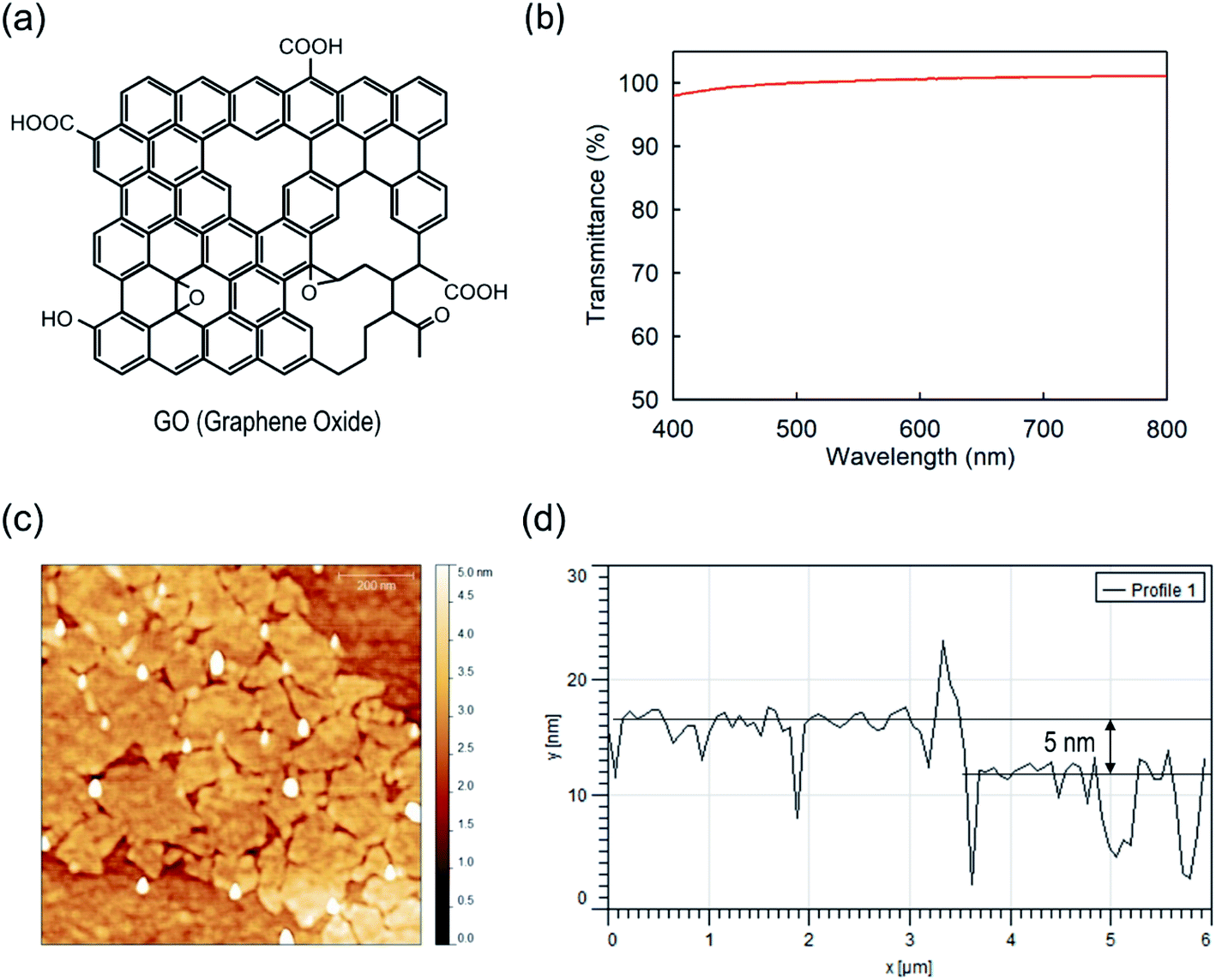 | ||
| Fig. 1 (a) Schematic illustration and (b) transmittance graphene oxide (GO) film spin-coated from a 2 mg mL−1 dense solution. (c) Topography image of GO flakes within a GO film spin-coated from a 0.5 mg mL−1 dense solution, and (d) its measured thickness (∼5 nm) by atomic force microscopy (AFM). | ||
To perform elemental analysis, XPS was conducted on the GO film (Fig. 2(a)). The low binding energy peak of the C 1s core located at 284.50 eV originates from the C–C bonding in the molecular structure of GO.49 The peaks at 286.79 and 288.31 eV originate from C–O and C![[double bond, length as m-dash]](https://www.rsc.org/images/entities/char_e001.gif) O bonding, respectively.49 As illustrated in Fig. 1(a), numerous C–O and CO bonds develop from the hydroxyl group (R–OH–), epoxy group (R–O–R), carboxyl group (R–COOH). After integrating the respective peaks, it is found that the respective atomic percentages of C–C, C–O, and CO bonds are 54.9, 39.4, and 5.7%, indicating sufficient oxidization of graphene to GO. To further validate the GO properties, the work function of the deposited GO film was measured and found to be approximately 4.6 eV (Fig. 2(b)), which is in good agreement with a former article.50
O bonding, respectively.49 As illustrated in Fig. 1(a), numerous C–O and CO bonds develop from the hydroxyl group (R–OH–), epoxy group (R–O–R), carboxyl group (R–COOH). After integrating the respective peaks, it is found that the respective atomic percentages of C–C, C–O, and CO bonds are 54.9, 39.4, and 5.7%, indicating sufficient oxidization of graphene to GO. To further validate the GO properties, the work function of the deposited GO film was measured and found to be approximately 4.6 eV (Fig. 2(b)), which is in good agreement with a former article.50
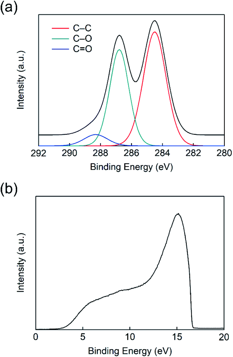 | ||
| Fig. 2 (a) X-ray photoelectron spectroscopy (XPS) and (b) ultraviolet photoelectron spectroscopy (UPS) measurement result of graphene oxide (GO). | ||
In the necessity of further fundamental analyses on the GO film, TGA (Fig. S2†), FTIR (Fig. S3†), and Raman spectroscopy (Fig. S4†) were conducted. In good agreement with the former GO-related TGA studies, it showed similar results upon increasing temperature. The first weight variation at 100 °C is ascribed to the removal of the moisture,51–55 the second drop from 150 °C to 220 °C is attributed to the removal of oxygen functional groups,51–56 and the last region above 550 °C is assigned to the removal of stable oxygen groups or combustion of remaining materials.52–56
Additional analyses of Fourier-transform infrared spectroscopy (FTIR) and Raman spectroscopy were conducted (Fig. S3 and S4†). In FTIR results (Fig. S3†), the GO film's absorption peaks at 1030 cm−1 (C–O), 1371 cm−1 (C–OH), 1724 cm−1 (CO), and a broadband between 3000 and 3500 cm−1 (O–H) indicate the effective functionalization of GO.57,58 Regarding the Raman spectroscopy result, clear D and G bands were observed (Fig. S4 and Table S1†), where D band indicates the disorder band caused by the graphite edges, and G band implies the in-phase vibration of the graphite lattice.59 The GO (1600 cm−1) showed a blue-shifted location of G band than the graphene (1590 cm−1), implying oxygenation of graphite and sp3 carbon atoms formation.59–61 In addition, the broadened D band of GO (FWHM = 140 cm−1) than graphene (FWHM = 100 cm−1) is ascribed to the reduction in sp2 domain size by the formation of defects, vacancies, and distortions upon oxidation.60 Furthermore, the relative peak intensity of the D band to G band (ID/IG) is increased from 0.985 to 1.037 when the graphene is functionalized to GO, implying the formation of oxygen-containing functional groups to the graphene plane.60
The J–V characteristics of OSCs with the different HELs were measured (Fig. 3(a, b) and Table 1). The photovoltaic parameters are abbreviated as follows: short-circuit current (JSC), open-circuit voltage (VOC), fill factor (FF), and power conversion efficiency (PCE). The performance of a device with PEDOT:PSS as an HEL showed photovoltaic parameters of JSC = 9.74 mA cm−2, VOC = 0.85 V, FF = 0.53, and PCE = 4.36%. For accurate comparison, a device without any HEL was fabricated, and its performance was measured to be JSC = 9.41 mA cm−2, VOC = 0.79 V, FF = 0.50, and PCE = 3.75%. Considering that the role of the HEL ranges from reducing the charge extraction barrier to accelerating the charge transport,62 it is quite intuitive that the JSC and VOC of the non-HEL device showed significant decreases, leading to a 21% lower PCE. On the other hand, OSCs with optimized GO conditions showed device characteristics comparable to those with PEDOT:PSS: JSC = 8.97 mA cm−2, VOC = 0.83 V, FF = 0.54, and PCE = 4.04%.
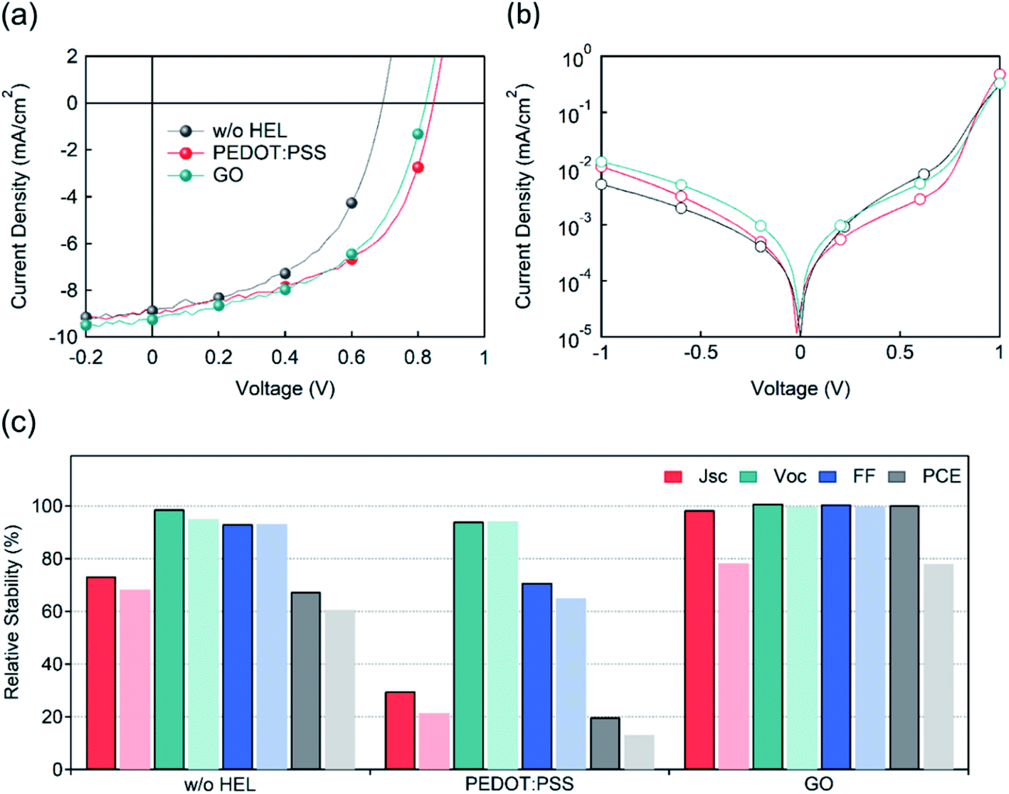 | ||
| Fig. 3 (a) Current density–voltage (J–V) characteristics, (b) dark current density, and (c) normalized values of the photovoltaic parameters of devices after 2 days (solid color with border) and 4 days (pale color without border) under ambient conditions. | ||
For further investigation, the GO was reduced with a significantly high temperature of 500 °C and applied to the device fabrication (Fig. S5†). In brief, it is reported that the GO can be effectively reduced with an extremely high temperature ranging from 300 °C to 600 °C.63 In Fig. S5,† the OSC with reduced GO, annealed at 500 °C after GO film formation, showed inferior performance of JSC = 6.34 mA cm−2, VOC = 0.405 V, FF = 0.369, and PCE = 0.948%. The variation is speculated to align with the former article reporting a significantly lower sheet resistance than GO,63 resulting in a severe charge extraction imbalance within the OSC.
| w/o HEL | PEDOT:PSS | GO | |
|---|---|---|---|
| JSC (mA cm−2) | 8.74 ± 0.55 (9.41) | 8.73 ± 0.71 (9.74) | 8.95 ± 0.23 (8.97) |
| VOC (V) | 0.71 ± 0.07 (0.79) | 0.85 ± 0.01 (0.85) | 0.81 ± 0.02 (0.83) |
| FF | 0.50 ± 0.01 (0.50) | 0.54 ± 0.01 (0.53) | 0.51 ± 0.03 (0.54) |
| PCE (%) | 3.14 ± 0.42 (3.75) | 3.99 ± 0.30 (4.36) | 3.71 ± 0.33 (4.04) |
Most importantly, the shelf lifetime varied significantly depending on the HEL (Fig. 3(c) and S6†). It is well known that OSCs with PEDOT:PSS are very vulnerable to degradation due to the acidic nature of the HEL, which deteriorates the adjacent active layer polymer and fullerene derivatives.19–24 In line with these studies, devices with PEDOT:PSS showed unstable JSC and FF, which decreased by 70% and 29%, resulting in a PCE drop of 80%, after 2 days. After 4 days of degradation, the PCE showed a total decrease of 87%. Although the device without an HEL showed relatively better stability than that with PEDOT:PSS, it still showed a PCE decrease of 40% after 4 days. On the other hand, the shelf lifetime of GO-based OSCs was measured to be much better than that under the other conditions. In particular, the GO-based device showed no decrease in PCE after 2 days, maintaining its fresh condition. After 4 days of degradation, the GO-based OSCs showed a PCE decrease of 22%. Therefore, we can conclude that GO is a great candidate for an OSC since it possesses comparable efficiency and significantly improved stability compared to PEDOT:PSS. For further confirmation, the 2 week shelf lifetime tendencies of the devices were measured (Fig. S7†), and GO-based OSC offered the most stable performance maintaining 50% of its initial value, which is a consistent result with the 4 day shelf lifetime evaluation (Fig. 3(c)).
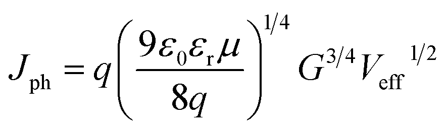
To analyze the charge transport characteristics within the OSC, we plotted the photocurrent (Jph) as a function of the effective voltage (Veff)64,65 from the equation,
 | (1) |
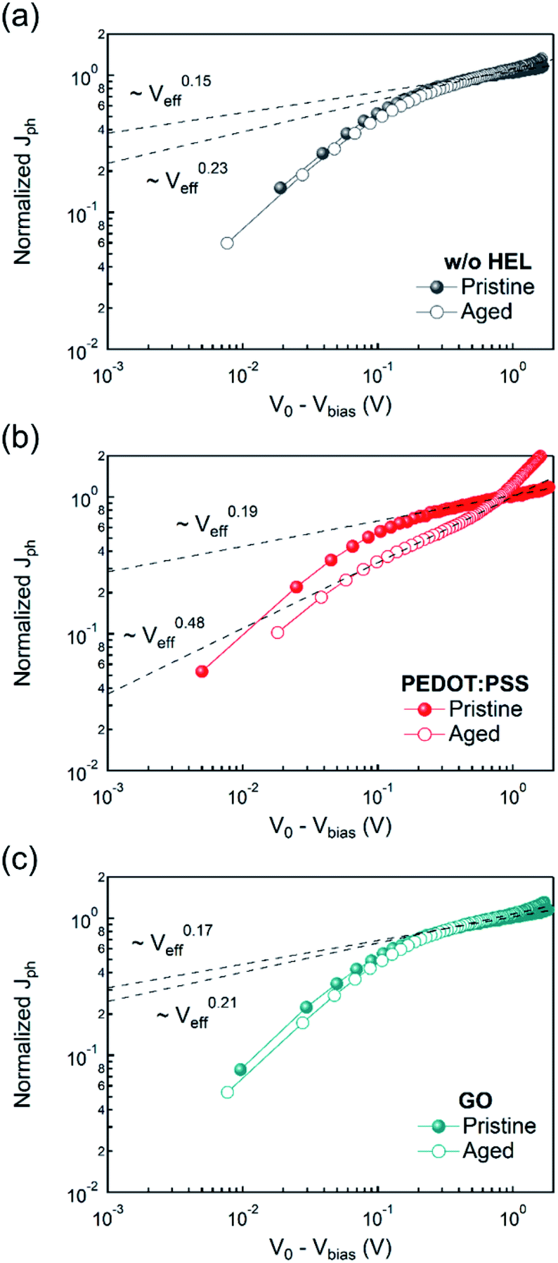 | ||
| Fig. 4 Photocurrent (Jph) as a function of effective voltage (Veff = V0 − Vbias) of the devices (a) without HEL, with (b) PEDOT:PSS, and (c) GO. | ||
To obtain further insight, impedance spectroscopy was performed on the devices with different HELs (Fig. 5). The electrical impedance spectroscopy-derived Cole–Cole plots have been widely used in solar cell research since they provide a compelling clue for determining the resistive characteristics. The Cole–Cole plots are widely used to extrapolate the recombination resistance (Rrec) through the low-frequency arc.67–72 While some of the studies related the decrease in Rrec to the enhanced charge transport,69,72 some of the articles reversely related the increase in Rrec to the reduced disadvantageous charge recombination at the interface70 or binary photoactive layer structure.68 Assuming the equivalent circuit as a series component of each component consisting of parallel resistance and capacitance units, Cole–Cole plots were measured, varying the frequency from 100 Hz to 50 MHz. Regardless of the HEL, they showed values of approximately 150 Ω at high frequencies, attributed to the same ITO series resistance. However, they differed significantly in the low-frequency resistance, Rrec. At low frequency, the non-HEL device showed the lowest resistance of 8.4 kΩ, while the plot with GO showed 126 kΩ at 100 Hz, and that with PEDOT:PSS showed 252 kΩ. First, the different resistances between the non-HEL and GO devices might originate from the GO layer effectively functioning as a dielectric layer.39,40 In addition, despite the small thickness of the GO layer of 5 nm (Fig. 1(d)), GO works well as a dielectric layer between the ITO and active layers and inhibits excessive charge migration or unfavorable charge quenching at the interface,43 which results in an increase in Rrec from 8.4 kΩ to 126 kΩ. Furthermore, the GO resistive component is smaller than the PEDOT:PSS resistive component because of the significantly tiny thickness of GO despite the high conductivity of PEDOT:PSS.
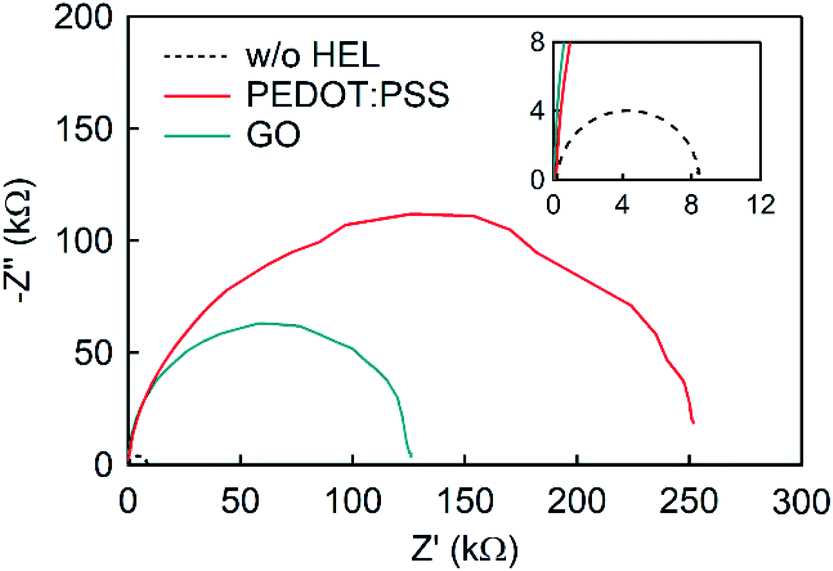 | ||
| Fig. 5 Cole–Cole plot measurement by impedance spectroscopy of devices with different HELs (inset: Cole–Cole plot of device without HEL). | ||
It is also crucial that the GO works well as a p-dopant into the PEDOT:PSS, which increases device performance. In Fig. 6, the photovoltaic parameters are plotted for the GO doping ratio ranging from 0.5 wt% to 5 wt%. According to a former article, mixing GO and PEDOT:PSS efficiently enhances the device characteristics by weakening the interaction between PEDOT and PSS, and forming an extra conductive network.73 In line with the studies, the mixed HEL showed an increased performance until some point. While JSC showed a steady increase, VOC showed the highest growth in 3 wt%, while FF decreased continuously. The combined index of all other 3 factors, the PCE, showed the optimized point at 1 wt% showing 24% improvement. However, for doping ratio exceeding 25 wt% to 75 wt%, the overall device performance showed a severe decrease (Fig. S8†), which is in line with the former articles reporting disadvantageous morphology variation upon excessive composite ratio.74 Therefore, if the stability is not a big concern, introducing the GO into the PEDOT:PSS with an optimized ratio will provide a proper method in increasing the efficiency of conventional optoelectronic devices.
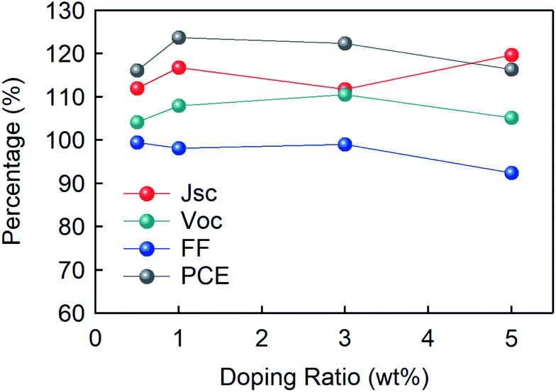 | ||
| Fig. 6 Normalized values of the photovoltaic parameters of devices with composite HIL as a function of the GO doping ratio from 0.5 wt% to 3 wt% compared to pristine PEDOT:PSS. | ||
Conclusions
In conclusion, we revealed that GO is one of the most appropriate candidates for HELs in OSCs. The topography images showed good surface properties without any aggregation of flakes and superior optical characteristics with high transmittance (Fig. 1). Furthermore, the initial performance of devices with GO and PEDOT:PSS showed almost comparable values (Fig. 3(a)), while they showed a massive difference in the shelf lifetime or stability in which the GO-based device exhibited a 6-fold increment compared to the PEDOT:PSS-based device (Fig. 3(c) and S6†). The enhanced shelf lifetime originated from the different degrees of involvement of space-charge limited region depending on the HELs (Fig. 4), which was supported by the following impedance spectroscopy (Fig. 5). Moreover, the mixed HEL with PEDOT:PSS and GO also offers increased efficiency, where the doping ratio of 5 wt% was found to be the optimized point with 24% improvement in PCE (Fig. 6). This study will provide practical and considerable insight into developing high-performing and substitutional HEL materials highly required in various optoelectronic areas.Author contributions
Jaehoon Kim: conceptualization, methodology, investigation, validation, writing – original draft. Ashis Kumar Sarker: conceptualization, methodology. Yeseul Park: formal analysis. Jeonghun Kwak: resources, writing – review & editing. Hyung-Jun Song: resources, supervision, validation, writing – review & editing. Changhee Lee: resources, supervision.Conflicts of interest
There are no conflicts to declare.Acknowledgements
This study was supported by the Research Program funded by the SeoulTech (Seoul National University of Science and Technology).Notes and references
- B. Lee, L. Lahann, Y. Li and S. R. Forrest, Sustainable Energy Fuels, 2020, 4, 5765–5772 RSC.
- N. C. Nicolaidis, P. V. Hollott, B. Stanwell, I. A. Gill, J. E. Bull, S. Bentsen, J. Iredale, T. M. Pappenfus, P. C. Dastoor, K. Feron, M. J. Griffith and N. P. Holmes, J. Chem. Educ., 2020, 97, 3751–3757 CrossRef CAS.
- S. Zhang, D. Tsonev, S. Videv, S. Ghosh, G. A. Turnbull, I. D. W. Samuel and H. Haas, Optica, 2015, 2, 607–610 CrossRef CAS.
- M. Kaltenbrunner, M. S. White, E. D. Głowacki, T. Sekitani, T. Someya, N. S. Sariciftci and S. Bauer, Nat. Commun., 2012, 3, 770 CrossRef PubMed.
- Y. Liu, N. Qi, T. Song, M. Jia, Z. Xia, Z. Yuan, W. Yuan, K.-Q. Zhang and B. Sun, ACS Appl. Mater. Interfaces, 2014, 6, 20670–20675 CrossRef CAS PubMed.
- J. Luke, L. Corrêa, J. Rodrigues, J. Martins, M. Daboczi, D. Bagnis and J.-S. Kim, Adv. Energy Mater., 2021, 11, 2003405 CrossRef CAS.
- R. Steim, T. Ameri, P. Schilinsky, C. Waldauf, G. Dennler, M. Scharber and C. J. Brabec, Sol. Energy Mater. Sol. Cells, 2011, 95, 3256–3261 CrossRef CAS.
- P. Vincent, S.-C. Shin, J. S. Goo, Y.-J. You, B. Cho, S. Lee, D.-W. Lee, S. R. Kwon, K.-B. Chung, J.-J. Lee, J.-H. Bae, J. W. Shim and H. Kim, Dyes Pigm., 2018, 159, 306–313 CrossRef CAS.
- Y. Wei, J. Yu, L. Qin, H. Chen, X. Wu, Z. Wei, X. Zhang, Z. Xiao, L. Ding, F. Gao and H. Huang, Energy Environ. Sci., 2021, 14, 2314–2321 RSC.
- L. Zhu, M. Zhang, G. Zhou, T. Hao, J. Xu, J. Wang, C. Qiu, N. Prine, J. Ali, W. Feng, X. Gu, Z. Ma, Z. Tang, H. Zhu, L. Ying, Y. Zhang and F. Liu, Adv. Energy Mater., 2020, 10, 1904234 CrossRef CAS.
- W. Yang, Z. Luo, R. Sun, J. Guo, T. Wang, Y. Wu, W. Wang, J. Guo, Q. Wu, M. Shi, H. Li, C. Yang and J. Min, Nat. Commun., 2020, 11, 1218 CrossRef CAS PubMed.
- L. Duan and A. Uddin, Adv. Sci., 2020, 7, 1903259 CrossRef CAS PubMed.
- L.-Y. Su, H.-H. Huang, Y.-C. Lin, G.-L. Chen, W.-C. Chen, W. Chen, L. Wang and C.-C. Chueh, Adv. Funct. Mater., 2021, 31, 2005753 CrossRef CAS.
- F. J. Lim, K. Ananthanarayanan, J. Luther and G. W. Ho, J. Mater. Chem., 2012, 22, 25057–25064 RSC.
- J. P. Thomas, L. Zhao, D. McGillivray and K. T. Leung, J. Mater. Chem. A, 2014, 2, 2383–2389 RSC.
- B. Kadem, W. Cranton and A. Hassan, Org. Electron., 2015, 24, 73–79 CrossRef CAS.
- G.-E. Kim, D.-K. Shin, J.-Y. Lee and J. Park, Org. Electron., 2019, 66, 116–125 CrossRef CAS.
- G. Kim, J. Lee, D. Shin and J. Park, IEEE Trans. Electron Devices, 2019, 66, 1041–1049 CAS.
- J. Cameron and P. J. Skabara, Mater. Horiz., 2020, 7, 1759–1772 RSC.
- B. Y. Kadem, M. Al-Hashimi, A. S. Hasan, R. G. Kadhim, Y. Rahaq and A. K. Hassan, J. Mater. Sci.: Mater. Electron., 2018, 29, 19287–19295 CrossRef CAS.
- J. J. Lee, S. H. Lee, F. S. Kim, H. H. Choi and J. H. Kim, Org. Electron., 2015, 26, 191–199 CrossRef CAS.
- M. Kim, M. Yi, W. Jang, J. K. Kim and D. H. Wang, Polymers, 2020, 12, 129 CrossRef CAS PubMed.
- H. Kim, S. Nam, H. Lee, S. Woo, C.-S. Ha, M. Ree and Y. Kim, J. Phys. Chem. C, 2011, 115, 13502–13510 CrossRef CAS.
- E. Voroshazi, B. Verreet, A. Buri, R. Müller, D. Di Nuzzo and P. Heremans, Org. Electron., 2011, 12, 736–744 CrossRef CAS.
- N. Yaacobi-Gross, N. D. Treat, P. Pattanasattayavong, H. Faber, A. K. Perumal, N. Stingelin, D. D. C. Bradley, P. N. Stavrinou, M. Heeney and T. D. Anthopoulos, Adv. Energy Mater., 2015, 5, 1401529 CrossRef.
- Z. Tang, A. Elfwing, J. Bergqvist, W. Tress and O. Inganäs, Adv. Energy Mater., 2013, 3, 1606–1613 CrossRef CAS.
- J. Meyer, S. Hamwi, M. Kröger, W. Kowalsky, T. Riedl and A. Kahn, Adv. Mater., 2012, 24, 5408–5427 CrossRef CAS PubMed.
- J. Meyer, M. Kröger, S. Hamwi, F. Gnam, T. Riedl, W. Kowalsky and A. Kahn, Appl. Phys. Lett., 2010, 96, 193302 CrossRef.
- S. Hamwi, J. Meyer, M. Kröger, T. Winkler, M. Witte, T. Riedl, A. Kahn and W. Kowalsky, Adv. Funct. Mater., 2010, 20, 1762–1766 CrossRef CAS.
- C. H. Cheung, W. J. Song and S. K. So, Org. Electron., 2010, 11, 89–94 CrossRef CAS.
- M. T. Greiner, L. Chai, M. G. Helander, W.-M. Tang and Z.-H. Lu, Adv. Funct. Mater., 2012, 22, 4557–4568 CrossRef CAS.
- J.-H. Huang, T.-Y. Huang, H.-Y. Wei, K.-C. Ho and C.-W. Chu, RSC Adv., 2012, 2, 7487–7491 RSC.
- H. Chang, Z. Sun, Q. Yuan, F. Ding, X. Tao, F. Yan and Z. Zheng, Adv. Mater., 2010, 22, 4872–4876 CrossRef CAS PubMed.
- U. A. Méndez-Romero, S. A. Pérez-García, X. Xu, E. Wang and L. Licea-Jiménez, Carbon, 2019, 146, 491–502 CrossRef.
- Y. Shen, S. Yang, P. Zhou, Q. Sun, P. Wang, L. Wan, J. Li, L. Chen, X. Wang, S. Ding and D. W. Zhang, Carbon, 2013, 62, 157–164 CrossRef CAS.
- G. Eda, G. Fanchini and M. Chhowalla, Nat. Nanotechnol., 2008, 3, 270–274 CrossRef CAS PubMed.
- H. A. Becerril, J. Mao, Z. Liu, R. M. Stoltenberg, Z. Bao and Y. Chen, ACS Nano, 2008, 2, 463–470 CrossRef CAS PubMed.
- L. F. Lima, C. F. Matos, L. C. Gonçalves, R. V. Salvatierra, C. E. Cava, A. J. G. Zarbin and L. S. Roman, J. Phys. D: Appl. Phys., 2016, 49, 105106 CrossRef.
- H. Liu, P. Xu, H. Yao, W. Chen, J. Zhao, C. Kang, Z. Bian, L. Gao and H. Guo, Appl. Surf. Sci., 2017, 420, 390–398 CrossRef CAS.
- D. Arthisree and G. M. Joshi, Mater. Res. Express, 2018, 5, 075304 CrossRef.
- W. S. Koh, C. H. Gan, W. K. Phua, Y. A. Akimov and P. Bai, IEEE J. Sel. Top. Quantum Electron., 2014, 20, 36–42 Search PubMed.
- G. Jo, S.-I. Na, S.-H. Oh, S. Lee, T.-S. Kim, G. Wang, M. Choe, W. Park, J. Yoon, D.-Y. Kim, Y. H. Kahng and T. Lee, Appl. Phys. Lett., 2010, 97, 213301 CrossRef.
- S.-S. Li, K.-H. Tu, C.-C. Lin, C.-W. Chen and M. Chhowalla, ACS Nano, 2010, 4, 3169–3174 CrossRef CAS PubMed.
- J. Nicasio-Collazo, J.-L. Maldonado, J. Salinas-Cruz, D. Barreiro-Argüelles, I. Caballero-Quintana, C. Vázquez-Espinosa and D. Romero-Borja, Opt. Mater., 2019, 98, 109434 CrossRef CAS.
- B.-Y. Wang, E.-S. Lee, Y.-J. Oh and H. W. Kang, RSC Adv., 2017, 7, 52914–52922 RSC.
- A. K. Sarker and J.-D. Hong, Langmuir, 2012, 28, 12637–12646 CrossRef CAS PubMed.
- N. I. Kovtyukhova, P. J. Ollivier, B. R. Martin, T. E. Mallouk, S. A. Chizhik, E. V. Buzaneva and A. D. Gorchinskiy, Chem. Mater., 1999, 11, 771–778 CrossRef CAS.
- W. S. Hummers and R. E. Offeman, J. Am. Chem. Soc., 1958, 80, 1339 CrossRef CAS.
- K. Krishnamoorthy, M. Veerapandian, K. Yun and S. J. Kim, Carbon, 2013, 53, 38–49 CrossRef CAS.
- J. Liu, M. Durstock and L. Dai, Energy Environ. Sci., 2014, 7, 1297–1306 RSC.
- M. Elshafie, M. G. Taha, S. M. Elhamamsy, Y. Moustafa and W. I. M. Elazab, Egypt. J. Pet., 2020, 29, 195–201 CrossRef.
- B. Y. Chang, N. M. Huang, M. N. An'amt, A. R. Marlinda, Y. Norazriena, M. R. Muhamad, I. Harrison, H. N. Lim and C. H. Chia, Int. J. Nanomed., 2012, 7, 3379–3387 CAS.
- E. Aliyev, V. Filiz, M. M. Khan, Y. J. Lee, C. Abetz and V. Abetz, Nanomaterials, 2019, 9, 1180 CrossRef CAS PubMed.
- A. Najjar, S. Sabri, R. Al-Gaashani, V. Kochkodan and M. A. Atieh, Appl. Sci., 2019, 9, 513 CrossRef CAS.
- N. Sharma, V. Sharma, Y. Jain, M. Kumari, R. Gupta, S. K. Sharma and K. Sachdev, Macromol. Symp., 2017, 376, 1700006 CrossRef.
- B. Gurzęda, P. Florczak, M. Wiesner, M. Kempiński, S. Jurga and P. Krawczyk, RSC Adv., 2016, 6, 63058–63063 RSC.
- B. D. Ossonon and D. Bélanger, RSC Adv., 2017, 7, 27224–27234 RSC.
- Y. Si and E. T. Samulski, Nano Lett., 2008, 8, 1679–1682 CrossRef CAS PubMed.
- K. N. Kudin, B. Ozbas, H. C. Schniepp, R. K. Prud'homme, I. A. Aksay and R. Car, Nano Lett., 2008, 8, 36–41 CrossRef CAS PubMed.
- S. Perumbilavil, P. Sankar, T. P. Rose and R. Philip, Appl. Phys. Lett., 2015, 107, 051104 CrossRef.
- F. T. Johra, J.-W. Lee and W.-G. Jung, J. Ind. Eng. Chem., 2014, 20, 2883–2887 CrossRef CAS.
- R. Steim, F. R. Kogler and C. J. Brabec, J. Mater. Chem., 2010, 20, 2499–2512 RSC.
- B. A. Chambers, M. Notarianni, J. Liu, N. Motta and G. G. Andersson, Appl. Surf. Sci., 2015, 356, 719–725 CrossRef CAS.
- V. D. Mihailetchi, J. Wildeman and P. W. M. Blom, Phys. Rev. Lett., 2005, 94, 126602 CrossRef CAS PubMed.
- W. E. I. Sha, X. Li and W. C. H. Choy, Sci. Rep., 2014, 4, 6236 CrossRef CAS PubMed.
- J. D. Morris, T. L. Atallah, C. J. Lombardo, H. Park, A. Dodabalapur and X.-Y. Zhu, Appl. Phys. Lett., 2013, 102, 033301 CrossRef.
- A. Guerrero, N. F. Montcada, J. Ajuria, I. Etxebarria, R. Pacios, G. Garcia-Belmonte and E. Palomares, J. Mater. Chem. A, 2013, 1, 12345–12354 RSC.
- M. Ramar, C. K. Suman, R. Manimozhi, R. Ahamad and R. Srivastava, RSC Adv., 2014, 4, 32651–32657 RSC.
- R. Sharma, H. Lee, V. Gupta, H. Kim, M. Kumar, C. Sharma, S. Chand, S. Yoo and D. Gupta, Org. Electron., 2016, 34, 111–117 CrossRef CAS.
- M.-J. Jin, J. Jo and J.-W. Yoo, Org. Electron., 2015, 19, 83–91 CrossRef CAS.
- B. Arredondo, B. Romero, G. Del Pozo, M. Sessler, C. Veit and U. Würfel, Sol. Energy Mater. Sol. Cells, 2014, 128, 351–356 CrossRef CAS.
- E.-P. Yao, C.-C. Chen, J. Gao, Y. Liu, Q. Chen, M. Cai, W.-C. Hsu, Z. Hong, G. Li and Y. Yang, Sol. Energy Mater. Sol. Cells, 2014, 130, 20–26 CrossRef CAS.
- H. S. Dehsari, E. K. Shalamzari, J. N. Gavgani, F. A. Taromi and S. Ghanbary, RSC Adv., 2014, 4, 55067–55076 RSC.
- Y. Yang, H. Deng and Q. Fu, Mater. Chem. Front., 2020, 4, 3130–3152 RSC.
Footnote |
| † Electronic supplementary information (ESI) available. See DOI: 10.1039/d1ra02452c |
| This journal is © The Royal Society of Chemistry 2021 |