DOI:
10.1039/D1RA02324A
(Paper)
RSC Adv., 2021,
11, 17230-17239
Electronic, mechanical, optical and photocatalytic properties of two-dimensional Janus XGaInY (X, Y ;= S, Se and Te) monolayers†
Received
24th March 2021
, Accepted 26th April 2021
First published on 11th May 2021
Abstract
Janus monolayers with breaking out-of-plane structural symmetries and spontaneous electric polarizations offer new possibilities in the field of two-dimensional materials. Due to the depletion of fossil fuels and serious environmental problems, there has been a growing interest in the conversion of water and solar energy into H2 fuels in recent years. In this research, Janus XGaInY (X, Y = S, Se and Te) monolayers are predicted as promising solar-water-splitting photocatalysts. Based on first-principles calculations, the electronic, mechanical, optical and photocatalytic properties of Janus XGaInY (X, Y = S, Se and Te) monolayers are investigated. These Janus monolayers are structurally stable semiconductors with indirect bandgaps, except for SGaInSe, SGaInTe, TeGaInS and SeGaInTe. Their energy bandgaps extend from 0.74 to 2.66 eV at a hybrid density functional level, which is crucial for broadband photoresponses. Moreover, these Janus monolayers not only show strong light absorption coefficients greater than 104 cm−1 in the visible and ultraviolet regions but possess suitable band edge positions for water splitting. Our findings reveal that these Janus monolayers have a potential for application in the fields of optoelectronic and photocatalysis.
Introduction
The isolation of the first ever two-dimensional (2D) graphene in 2004 (ref. 1) opened up a new pathway for materials scientists to search for new graphene-like 2D materials. Due to extensive studies on graphene, 2D layered materials, including MXenes,2 phosphorene,3 analogous binary materials,4 transition metal dichalcogenides (TMDCs),5,6 Janus TMDCs,7,8 silicene,9–11 etc., have been theoretically predicted and experimentally synthesized for various interesting applications in photocatalysis and optoelectronic devices.12,13 Among them, the semiconductor group-III monochalcogenides have been comprehensively studied for their prospective applications in the field, such as in the conversion of solar energy.14,15 Recently, experimental efforts have been assumed to fabricate these group-III monochalcogenides in the form of single layers. To date, single layers of GaS, GaSe,16,17 GaTe18,19 and InSe20,21 have been successfully synthesized and comprehensively examined.
The quantum confinement of materials from bulk (3D) to a single layer (2D) counterpart dramatically changes the mechanical and electronic properties of materials. For example, the electronic properties of 2D MoS2 exhibit a larger bandgap than its 3D counterpart, which has been confirmed experimentally.22,23 Commonly, 2D materials can easily be strained for mechanical properties. For example, single-layer graphene can tolerate strain up to 25%,24 which is significantly greater than that of graphite, whose maximum elastic strain limit is 0.1%.25 The development of 2D materials is not limited to mono-elemental or binary systems but they have been followed by the fabrication of ternary structures in alignment with advancements in experimental methods. Lu et al. have described the production of ternary MoSSe monolayers by substituting all of the S atoms on one side of MoS2 with Se atoms.7 By this approach, the out-of-plane mirror symmetry is broken, resulting in new properties different than the binary counterpart. Consequently, the Janus MoSSe monolayer has been synthesized by substituting one layer of Se atoms of MoSe2 with S atoms via controlled sulfurization.26 The resultant structure has characteristic Raman peaks differentiating it from the MoS2 and MoSe2 monolayers. These efforts are not limited to transition metal dichalcogenides but have also been extended to different classes including the ternary group-III monochalcogenides. The Janus In2SSe monolayer27 has been predicted recently and an indirect-direct bandgap transition due to broken vertical symmetry has been reported. The other ternary derivatives of group-III monochalcogenides have been also theoretically investigated and they have been suggested as piezoelectric materials with high piezoelectric coefficients.28 Bui et al. studied the structural, electronic, and optical properties of Janus Ga2SSe, Ga2STe and Ga2SeTe monolayers29 and compared the acquired electronic band gaps with their binary analogs. In the interpretation of these uncommon properties, it is necessary to determine the potential of single layer Janus XGaInY materials for solar energy conversion and photocatalysis.
The generation of hydrogen by photocatalytic water splitting is an effective technique for the conversion of solar energy. When the sunlight falls on a semiconductor photocatalyst, photons generate electron–hole pairs. The excited electron and hole are responsible for the hydrogen reduction and oxidation reactions, respectively. To facilitate photocatalytic activity, a photocatalyst must satisfy at least two conditions. First, the bandgap must be equal to or greater than 1.23 eV, which is the free energy for water splitting. Second, the conduction band minimum (CBM) and valence band maximum (VBM) of photocatalysts should lie higher and lower than the reduction (H+/H2) and oxidation (O2/H2O) potentials, respectively.30 To break the bandgap limitations of photocatalysts for water splitting, a new mechanism has been proposed.31 The vertical intrinsic electric field, taking into account two-dimensional In2Te3 with the bandgap of 1.14 eV, can absorb infrared light to drive complete water splitting.32 In addition to satisfying the aforementioned criteria of electronic structure, the Janus XGaInY monolayers considered in this work have a great advantage in photocatalytic applications. The nature of these 2D materials means that they increase surface area and reduce the distance that the generated electrons and holes have to migrate, minimizing the recombination rate of electron–hole pairs, which potentially enhances their photocatalytic activity.33,34
The successful implementation of Janus monochalcogenides29 has produced a new strategy for designing materials with amazing properties and has stimulated research interest in other Janus monolayers. With this in mind, we studied a new group of Janus monochalcogenides based on XGaInY (X, Y= S, Se and Te) from GaS, which may lead to new consequences because of their remarkable electronic, optical and photocatalytic properties. Here, we investigated the electronic, mechanical, optical and photocatalytic properties of XGaInY monolayers by using first-principles calculations. We found that these monolayers are mechanically and dynamically stable, which can be confirmed experimentally. We showed that these monolayers absorbed the visible spectrum of solar energy and enhanced photocatalytic activity.
Methodology
The density functional theory (DFT) calculations were performed in the plane wave Vienna ab initio simulation package (VASP).35 To optimize the structure geometry, the projected augmented wave method36 and generalized gradient approximation (GGA) functional of Perdew, Burke, and Ernzerhof (PBE) were used.37 To overcome the underestimation of the bandgap in PBE calculations, we used the HSE06 functional38 to obtain a more precise electronic structure. The cut-off energy of 500 eV was used throughout the calculations. A gamma-centered 27 × 27 × 1 k-mesh was sampled in the Brillouin zone for structural relaxation and 15 × 15 × 1 k-mesh was used for HSE06 calculations. A 25 Å vacuum was applied along the vertical direction to avoid the interaction between the adjacent periodic images. The convergence criteria for force and energy during the relaxation of the structures were set to 0.001 eV Å−1 and 10−5 eV, respectively. Phonon dispersion calculations were conducted by using a small displacement technique, which is employed in the PHONOPHY code.39
Results and discussion
Atomic structure and stability
The crystal structures of Janus XGaInY (X, Y = S, Se and Te) monolayers consist of four sublayers stacked in the sequence X–Ga–In–Y, as depicted in Fig. 1. The atomic structure of the GaS monolayer is also plotted for comparison. All the Janus monolayers are inherited from the binary counterpart GaX (X = S, Se and Te), which belong to a space group (no. 187). The Janus structures were produced as follows: in the first pattern we only replaced one of the two sublayers of Ga with indium (In) atoms in parent monolayers, resulting in the formation of Janus SGaInS, SeGaInSe and TeGaInTe monolayers, as shown in Fig. 1(b–d). In the second pattern, the inner two layers of Ga and In atoms remained unchanged, only the S atoms of the top layer of GaS were replaced by Se atoms to give the SGaInSe monolayer. Proceeding by the same method, we generated the other SeGaInS, SGaInTe, TeGaInS, SeGaInTe and TeGaInSe Janus monolayers represented in Fig. 1(e–j). The optimized bond lengths, lattice constants and thickness of all Janus monolayers are tabulated in Table 1. To check the stability, i.e., whether these Janus monolayers can stay stable in freestanding environments, deserves further investigation.
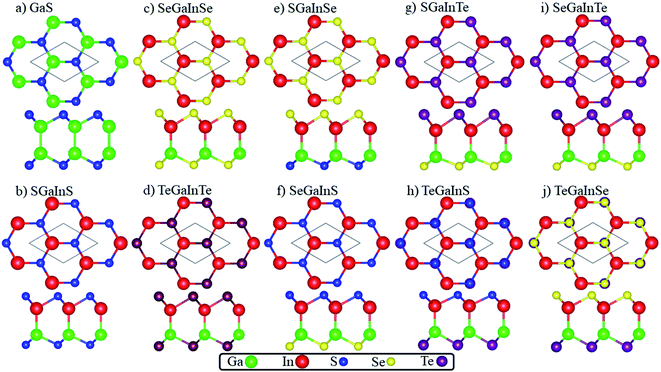 |
| | Fig. 1 Top and side view of (a) GaS, (b) SGaInS, (c) SeGaInSe, (d) TeGaInTe, (e) SGaInSe, (f) SeGaInS, (g) SGaInTe, (h) TeGaInS, (i) SeGaInTe and (j) TeGaInSe. | |
Table 1 Bond lengths of all Janus monolayers
| Structures |
d(Ga–Ga) (Å) |
d(Ga–In) (Å) |
d(Ga–S) (Å) |
d(Ga–Se) (Å) |
d(Ga–Te) (Å) |
d(In–S) (Å) |
d(In–Se) (Å) |
d(In–Te) (Å) |
| GaS |
2.47 |
— |
2.35 |
— |
— |
— |
— |
— |
| SGaInS |
— |
2.65 |
2.40 |
— |
— |
2.51 |
— |
— |
| SeGaInSe |
— |
2.65 |
— |
2.53 |
— |
— |
2.64 |
— |
| TeGaInTe |
— |
2.64 |
— |
— |
2.74 |
— |
— |
2.85 |
| SGaInSe |
— |
2.65 |
2.43 |
— |
— |
— |
2.62 |
— |
| SeGaInS |
— |
2.65 |
— |
2.51 |
— |
2.53 |
— |
— |
| SGaInTe |
— |
2.64 |
2.49 |
— |
— |
— |
— |
2.80 |
| TeGaInS |
— |
2.65 |
— |
— |
2.67 |
2.57 |
— |
— |
| SeGaInTe |
— |
2.65 |
— |
2.59 |
— |
— |
— |
2.81 |
| TeGaInSe |
— |
2.65 |
— |
— |
2.70 |
— |
2.68 |
— |
Therefore, we first calculated the binding energy per atom using the following formula:
| | |
Eb = (Etotal − nEGa − nEIn − nES − nESe − nETe)/N
| (1) |
where
Etotal is the total energy of the pristine and Janus monolayers.
EGa, EIn, ES, ESe and
ETe are the total energies of an individual atom with (
n = 1, 2 …) in the system, while
N is the total number of atoms in the system. The calculated binding energies are listed in
Table 2, which support that the XGaInY monolayers have sensible thermodynamic stability. To confirm the kinetic stability of the Janus XGaInY monolayers, we did phonon spectrum calculations. The phonon spectra of the monolayers are depicted in
Fig. 2. One can see that there are no imaginary frequencies in all monolayers, except that SGaInTe has a very small imaginary frequency, which is in the expectable error range. The results revealed that all monolayers are kinetically stable. Furthermore, we checked the mechanical stability of these monolayers by determining their elastic constants, as listed in Table S1 of the ESI.
† All the monolayers satisfy the Born–Huang criteria
40,41 for mechanical stability. The kinetic, thermodynamic and mechanical stability of these monolayers reveal that they can be applied in further experiments.
Table 2 Calculated lattice constants (a), band gaps, thicknesses (h), binding energies (Eb), band edge positions (CBM&VBM (both sides)), effective masses and relative effective masses (R) of Janus GaInXY monolayers
| Structures |
a (Å) |
EPBEg (eV) |
EHSEg (eV) |
h (Å) |
Eb eV |
CBM |
VBM |

(mo) |

(mo) |
R |
Direct band gap |
| GaS |
3.63 |
2.37 |
3.26 |
4.64 |
−0.65 |
−3.63 |
−6.90 |
1.41 |
3.62 |
5.11 |
No |
| SGaInS |
3.76 |
1.75 |
2.66 |
4.93 |
−0.55 |
−4.51 |
−7.17 |
1.28 |
4.78 |
3.73 |
No |
| −4.81 |
−7.47 |
| SeGaInSe |
3.94 |
1.38 |
2.19 |
5.12 |
−0.51 |
−4.24 |
−6.44 |
0.93 |
4.70 |
5.05 |
No |
| −4.37 |
−6.57 |
| TeGaInTe |
4.25 |
1.19 |
1.84 |
5.33 |
−0.33 |
−4.04 |
−5.88 |
0.64 |
2.87 |
4.49 |
No |
| −4.02 |
−5.86 |
| SGaInSe |
3.84 |
1.27 |
2.13 |
5.04 |
−0.52 |
−4.45 |
−6.59 |
1.16 |
5.15 |
4.43 |
Yes |
| −4.29 |
−6.43 |
| SeGaInS |
3.86 |
1.64 |
2.52 |
5.02 |
−0.54 |
−3.93 |
−6.45 |
1.01 |
4.72 |
4.67 |
No |
| −4.38 |
−6.90 |
| SGaInTe |
4.01 |
0.16 |
0.74 |
5.13 |
−0.34 |
−4.95 |
−5.68 |
1.36 |
3.25 |
2.39 |
Yes |
| −4.45 |
−5.08 |
| TeGaInS |
4.03 |
1.42 |
2.20 |
5.08 |
−0.43 |
−3.59 |
−6.15 |
1.03 |
3.06 |
2.97 |
Yes |
| −4.30 |
−6.50 |
| SeGaInTe |
4.09 |
0.44 |
1.12 |
5.24 |
−0.38 |
−4.73 |
−5.85 |
0.86 |
3.29 |
3.82 |
Yes |
| −4.41 |
−5.53 |
| TeGaInSe |
4.12 |
1.45 |
2.19 |
5.19 |
−0.43 |
−3.77 |
−5.96 |
0.79 |
3.60 |
4.83 |
No |
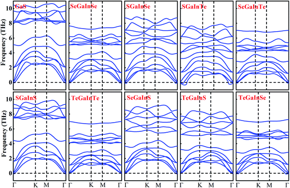 |
| | Fig. 2 Phonon dispersions of GaS and Janus XGaInY monolayers. | |
Electronic properties
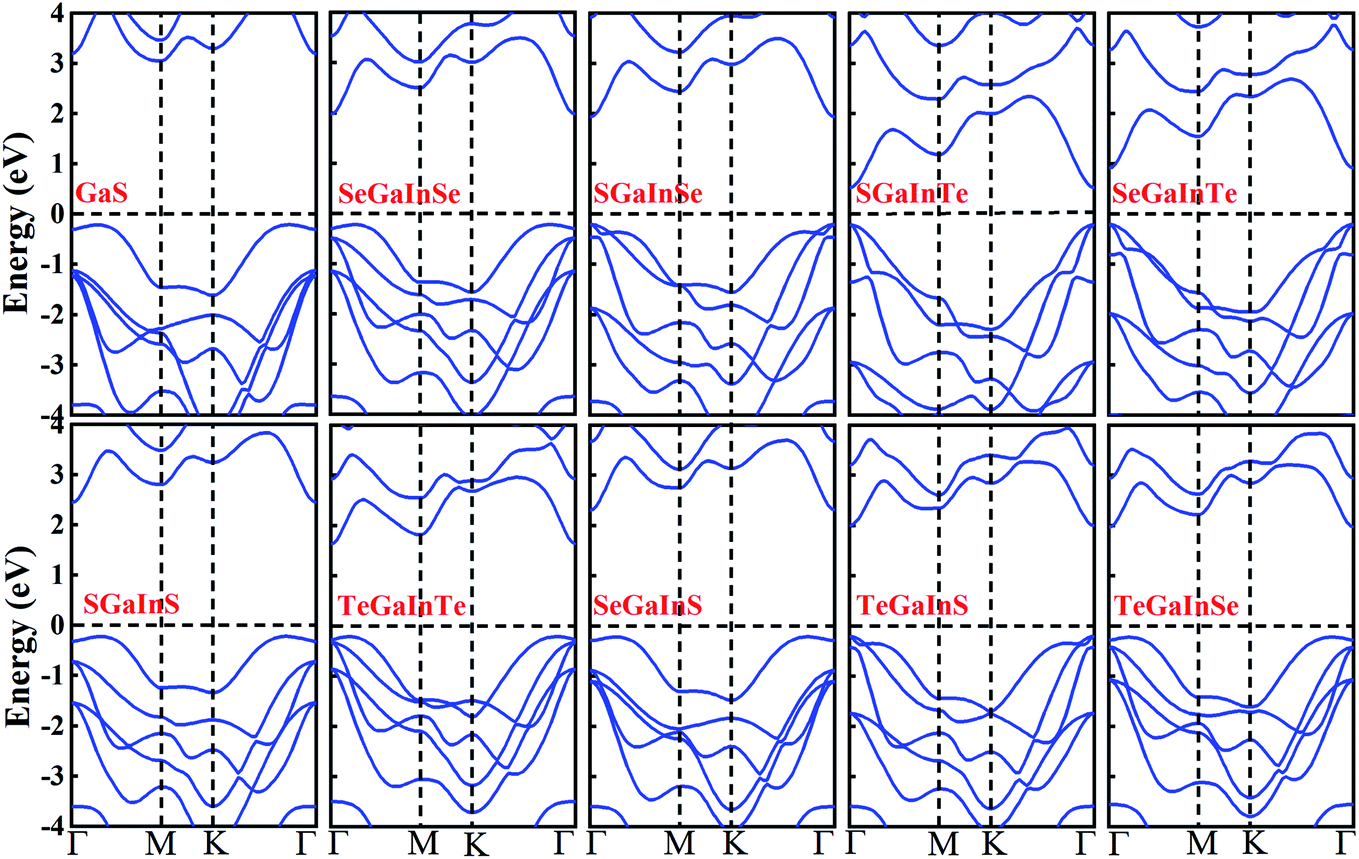
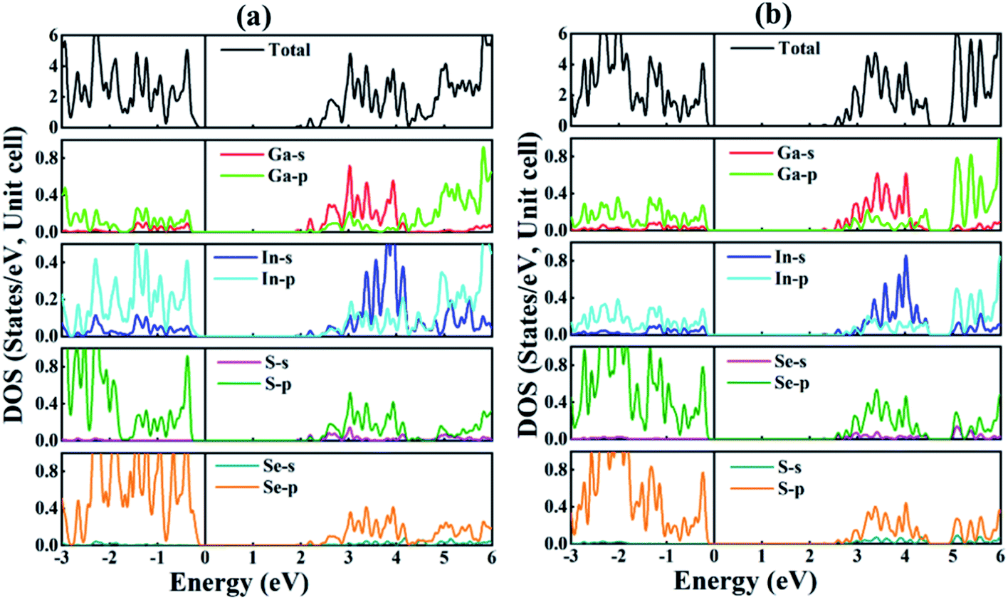
After confirming the formation and stability prospects of Janus XGaInY monolayers, we explored their electronic properties accordingly. To get a more accurate band structure of these Janus monolayers, the hybrid functional (HSE06) was employed. The calculated electronic band structures of the Janus monolayers showed semiconductor behaviour with bandgaps ranging from 0.74 to 2.66 eV. The lattice constant and bandgap of GaS are quite consistent with previous studies,42 which confirms the reliability of our work. The bandgaps calculated using PBE and HSE06 are listed in Table 2. The Janus SGaInSe, SGaInTe, TeGaInS and SeGaInTe monolayers are direct bandgap semiconductors at Γ point with 2.13 eV, 0.74 eV, 2.20 eV and 1.11 eV, respectively, as presented in Fig. 3. The GaS monolayer is an indirect semiconductor with a conduction band minimum (CBM) at the M point and valence band maximum (VBM) at the Γ–M path, which is consistent with literature.42 The CBMs of Janus SGaInS, SeGaInSe, TeGaInTe, SeGaInS and TeGaInSe monolayers are located at the Γ point, which is depicted in Fig. 3 and the VBMs are located at the Γ–K path, except for SGaInS, whose VBM is at the Γ–M path. To further investigate their electronic structures, we calculated the partial density of states (PDOS), as shown in Fig. 4 and S1–S8.† The VBMs of SGaInS, SeGaInSe, TeGaInTe, SeGaInS and TeGaInSe are mainly contributed by the p-states of ‘Ga’, ‘In’ and chalcogen atoms, while SGaInTe, TeGaInS, and SeGaInTe monolayers are dominated by Te-p states with the minor contribution of In-p, Ga-p and In-p states, respectively. The valence band edge of SGaInSe occurs due to the Se-p state, as presented in Fig. 4(a). On the other hand, the CBM of all monolayers are contributed by the Ga-s, In-s and p-states of chalcogen atoms.
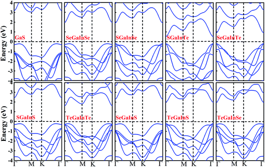 |
| | Fig. 3 The electronic band structures of GaS and Janus XGaInY monolayers. | |
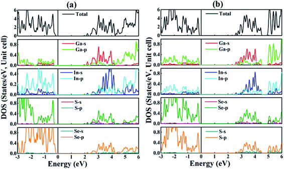 |
| | Fig. 4 Density of states of (a) SGaInSe (b) SeGaInS. | |
Electron localization function (ELF)
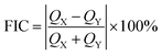
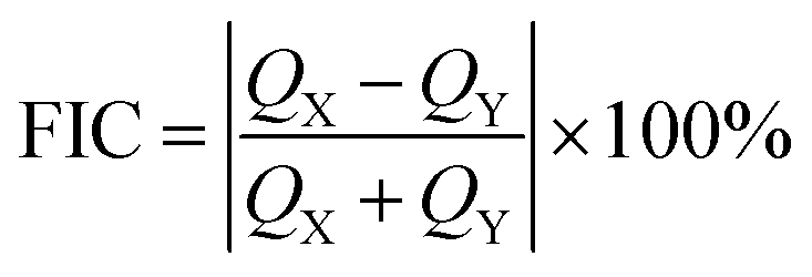
To understand and analyze the nature of chemical bonding, we have calculated the electron localization function (ELF)43 of GaS and Janus monolayers. The evaluated ELF is projected on the (110) plane, which passes through all the atoms in the system, as shown in Fig. S9.† ELF can be described in real space in the form of a contour plot, and its value ranges from 0 to 1, where the values of 0 (blue area) and 1 (red area) correspond to delocalized and fully localized electrons, respectively, and 0.5 (green area) denotes the distribution of electron gas-like pairs. From Fig. S9,† the maximum ELF value is around the S, Se and Te atoms, indicating that the electron density around these atoms is completely localized. Furthermore, the ELF values between Ga–Ga and Ga–In atoms demonstrate that they are covalently bonded. In addition, this property of the system can be further verified by fractional ionic character (FIC),44,45 which is given as follows:| |
 | (2) |
where QX and QY are the effective charges of Ga, In and In, S, Se, Te atoms, respectively. According to the above formula, the lower and higher values of FIC correspond to the covalent and ionic bond character, respectively. The calculated values of FIC for GaS and all Janus monolayers are listed in Table S2.† From the calculated FIC values, it is clear that the Ga–In atoms are bonded together through a strong covalent bond. Our results are quite consistent with previous studies.46
From ELF combined with Bader charge analysis (listed in Table S2†), we can further explain the stability of Janus XGaInY monolayers in water, which is a very important factor for an efficient water-splitting photocatalyst. For example, the C2N monolayer is unsolvable in water due to strong covalent bonds. It is clear that ionic compounds show good solvability in water because of a large amount of charge transfer between the atoms and the substantial polarization of chemical bonds. Fig. S10† shows that the strong ELF value appears around S, Se and Te atoms of GaS and Janus monolayers, while an ELF value of ∼0.5 appears about Ga and In atoms, respectively. This indicates that GaS and Janus monolayers show partial ionic character. On the other hand, earlier theoretical studies predicted that the WS2 monolayer would exhibit poor solvability due to partial ionic character, which was already confirmed by experiment.47,48 Based on Bader charge analysis, the charge transfer from tungsten (W) atom to S atom was 0.66e in the WS2 monolayer. One can see that our Bader charge analysis for GaS and Janus XGaInY monolayers are quite analogous with that of the WS2 monolayer, as presented in Table S2.† Hence, we proposed that our designed Janus XGaInY monolayers could show good stability in water.
Mechanical properties
In order to discuss the mechanical stability, elastic constants of Janus XGaInY monolayers were systematically investigated, as listed in Table S1.† Due to hexagonal symmetry, we evaluated only three independent C11, C12 and C66 elastic constants. The in-plane Young's modulus (Y) and Poisson's ratio (ν) were calculated byY = (C112 − C122)/C11 and ν = C12/C11, respectively, as shown in Table S1.† Our calculated value of Poisson's ratio (ν) is comparable to the previous study.49 The stiffness of the materials can be described by Young's modulus (Y). Stiffness is the rigidity of the material, which resists distortion under the effect of external forces. The higher the Young's modulus, the stiffer the material. The brittleness and ductility criteria of the materials can be judged from Poisson's ratio.50 For a brittle material, the value of Poisson's ratio should below 0.33, otherwise the material will be ductile. The results in Table S1† show that Janus XGaInY monolayers are brittle materials that could have great potential in many fields, such as electronic and photovoltaic applications.
The effective mass changes of charge carriers
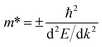
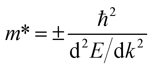
To determine the charge separation efficiency, we investigated the relative effective mass of photo-generated charge carriers. Based on calculated electronic band structures, the effective mass of electrons and holes of GaS and Janus XGaInY monolayers were evaluated by the parabolic fitting of the CBM and VBM, separately. Effective masses of electrons and holes were calculated using the following equation:51| |
 | (3) |
where m* is the effective mass and d2E/dk2 is the second-order derivative in a quadratic fit of E(k) curves for the band edges.
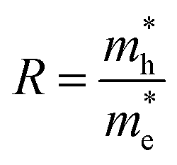
The charge separation efficiency is calculated from the relative effective masses of electrons and holes. In photocatalysis, the relative ratio (R) of the effective masses plays an important role, which is calculated by the following equation.52–54
| |
 | (4) |
The higher value of R shows that the photo-induced electron–hole pairs have enough affinity to separate, which enhances the photocatalytic performance. The effective masses of photo-generated electrons and holes, as well as the R values of Janus XGaInY monolayers are listed in Table 2. The effective mass of electrons  of all Janus monolayers is smaller than as compared to BiVO4, TiO2 and g-C3N4,52,53,55 while the R values of our Janus monolayers are greater than these photocatalysts, which already have a high photocatalytic performance. When photo-generated charge carriers have a smaller effective mass, it means that the charge carriers have a greater capability to reach the surface and take part in the reaction, which enhances the photocatalytic activity. Therefore, the photocatalytic performance of our designed Janus monolayers was higher than that of the three photocatalysts mentioned above.
Optical properties
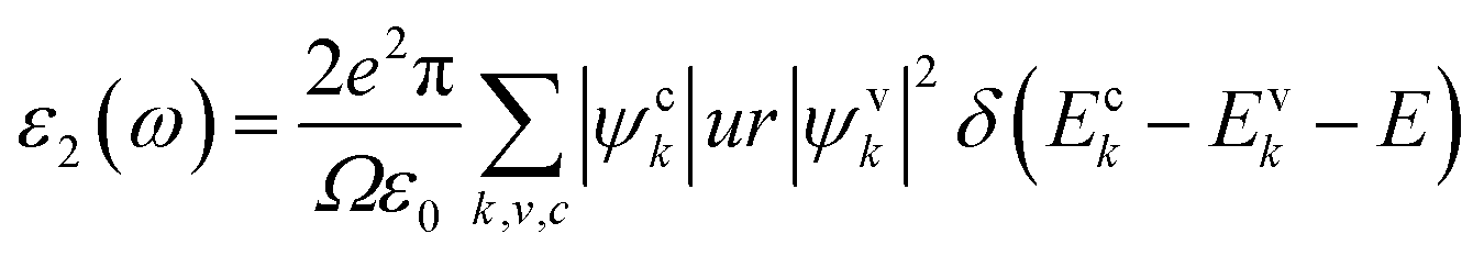
The optical properties of materials are necessary to classify the prospective applications of these materials in electronic optical devices. A suitable band alignment and an appropriate bandgap are important because a photocatalytic material absorbs a significant portion of the incoming solar spectrum. Due to external electromagnetic radiation, the linear response of the system is described by the complex dielectric function ε(ω) = ε1(ω) + iε2(ω), where ε1(ω) and ε2(ω) are the real and imaginary parts of a dielectric function, respectively. The real part ε1(ω) can be obtained from the Kramer–Kronig relationship.56 The imaginary part ε2(ω) is obtained by calculating the matrix element between the electronic wave functions of the unoccupied states and occupied states according to the selection rule of the electronic transition. The imaginary part ε2(ω) can be expressed as follows:57,58| |
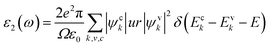 | (5) |
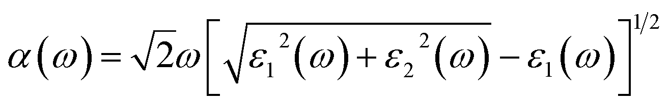
where e and u are the electronic charge and polarization vector of an electric field. The ψck and ψvk are the conduction band (CB) and valence band (VB) wave functions. The absorption coefficient α(ω) can be obtained from the following equation.59| |
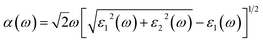 | (6) |
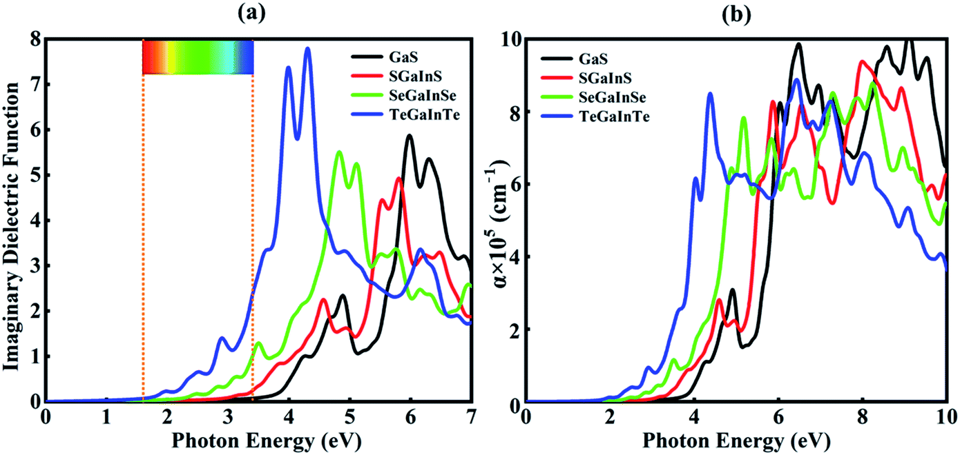
The imaginary part of the dielectric function is directly linked to the electronic structure and optical response of the materials. In this study, we have calculated the imaginary part and absorption coefficient of Janus XGaInY monolayers. The imaginary part of the GaS monolayer is also plotted for comparison. The calculated imaginary parts are depicted in Fig. 5(a) and 6(a). All Janus monolayers have appropriate band gaps of 0.74–2.66 eV, implying that there is a substantial possibility for optical absorption in the visible region of the solar spectrum. The imaginary part of the dielectric functions in Fig. 5(a) shows that both the GaS and SGaInS monolayers can hardly absorb the visible light and show the absorption in the ultraviolet (UV) region, while SeGaInSe and TeGaInTe have significant absorption peaks in the visible and ultraviolet regions of light. Interestingly, SGaInSe, SeGaInS, SGaInTe, TeGaInS, SeGaInTe and TeGaInSe have also harvested large portions of the visible spectrum, as shown in Fig. 6(a). Since visible light accounts for 50% of the solar spectrum, the optical absorption of all our designed Janus monolayers would guarantee high efficiency in the harvesting of solar energy. In order to better understand the performance under light, we also investigated the optical absorption coefficient as shown in Fig. 5(b) and 6(b). The decay of light intensity spreading in a unit length of the medium is referred to as the absorption coefficient. SeGaInSe and TeGaInTe are shown in Fig. 5(b), while SGaInSe, SeGaInS, SGaInTe, TeGaInS, TeGaInTe and TeGaInSe are shown in Fig. 6(b). Janus monolayers show a strong absorption coefficient up to 104 cm−1 and strong absorption peaks in the visible region of light. The results indicate that these Janus monolayers would exhibit better performance in the fields of optoelectronics and photocatalytic water splitting.
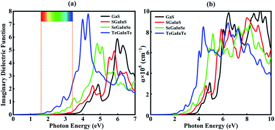 |
| | Fig. 5 Imaginary dielectric functions (a) and absorption coefficients (b) for the GaS, SGaInS, SeGaInSe and TeGaInTe monolayers. | |
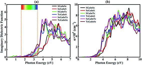 |
| | Fig. 6 Imaginary dielectric functions (a) and absorption coefficients (b) for the Janus SGaInSe, SeGaInS, SGaInTe, TeGaInS, SeGaInTe and TeGaInSe monolayers. | |
Photocatalysis
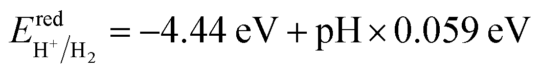
The photocatalytic performance of a photocatalyst could be determined by the CBM and VBM positions with respect to the redox potential levels of water. For overall water splitting, the basic requirement for photocatalysts is that the band edge potentials must straddle the water redox potentials; i.e., the CBM must be at a higher position than H+/H2 (reduction potential) and the VBM should be at a lower position than H2O/O2 (oxidation potential). The water redox potential is very closely related to the pH. The pH-dependent oxidation potential for O2/H2O and the reduction potential for H+/H2 are further evaluated by the following equations:12,60,61| |
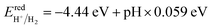 | (7) |
| |
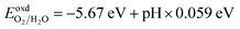 | (8) |
The electrostatic potential difference was detected at the surface of two dimensional Janus monolayers,32 which have different values for oxidation potential O2/H2O and reduction potential H+/H2. The dipole correction62 takes an important part in the perpendicular distribution of electrostatic potential to the XGaInY monolayers. It was found that there is a clear vacuum level difference on both sides of the Janus XGaInY monolayers with the dipole correction, while in the pristine monolayer there was no difference, as presented in Fig. S10.† The Janus layered structures retained a natural intrinsic electric field due to the mirror asymmetry, so for asymmetric structures, the dipole correction must be considered.
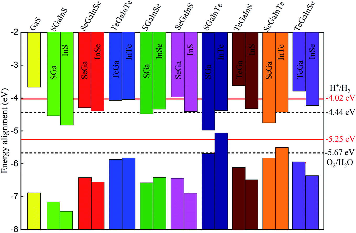
Therefore, to find the photocatalytic performance of Janus XGaInY monolayers, we considered the dipole correction. The evaluation of the band edge positions of the pristine and Janus XGaInY monolayers with reference to vacuum levels of both sides of Janus monolayer at pH = 0 and pH = 7 are depicted in Fig. 7. The calculated band edge positions of GaS are consistent with previous theoretical studies,42,63 which confirms the reliability of the adopted theoretical approach. The computed band edge positions of GaS and both sides of the Janus monolayers are listed in Table 2. At pH = 0, all the Janus monolayers are capable of dissociating water into H+/H2, except for SGaInS. The CBM of the Janus SGaInSe, −4.45 eV, with reference to the vacuum level of the SGa side, is lower than the reduction potential (−4.44 eV), while it shifted to −4.29 eV with reference to the vacuum level of the InSe side. Thus, the Janus SGaInSe monolayer is photocatalytically active for water splitting due to the intrinsic electric field. The same properties exist in other Janus monolayers, just like SGaInTe and SeGaInTe. On the other hand, all the monolayers are capable of oxidizing water to O2/H2O at pH = 0 and pH = 7, while at pH = 7 the Janus monolayers fail to dissociate water into H+/H2, except for SeGaInS, TeGaInS and TeGaInSe. The SGaInSe, SGaInTe, TeGaInS and SeGaInTe are direct bandgap Janus monolayers, which could be better for photocatalysis as compared to other indirect bandgap Janus monolayers. The band edge positions of the GaS monolayer were also plotted for comparison. We can see that the band edge positions of the GaS monolayer are favourable for full water splitting at pH = 0 and 7, but the electronic bandgap is greater than 3.2 eV, making it unsuitable for harvesting a wide range of the solar spectrum, which limits the potential conversion efficiency.64,65 Our proposed Janus monolayers could provide valuable direction for experimental synthesis and their potential applications in the field of photocatalysis.
 |
| | Fig. 7 Valence and conduction band edge positions of the GaS and Janus XGaInY monolayers relative to the vacuum level. The standard redox potentials for water splitting at pH = 0 (black dotted lines) and pH = 7 (red lines) are shown for comparison. | |
Conclusions
Using first-principles calculations, we have evaluated the electronic, mechanical, optical and photocatalytic properties of Janus XGaInY monolayers. Our findings indicate that all the Janus monolayers are kinetically, thermodynamically and mechanically stable. These Janus monolayers showed semiconducting behaviour with an indirect bandgap, while SGaInSe, SGaInTe, TeGaInS and SeGaInTe exhibited direct appropriate bandgaps, which is a good sign for optoelectronic applications. The calculated electronic band structures were evaluated by the HSE06 functional with the bandgap ranging from 0.74 to 2.66 eV. Interestingly, all the Janus monolayers can harvest big portions of the visible solar spectrum, except SGaInS, which hardly absorbs visible light. The band edge positions of these Janus monolayers are suitable for photocatalytic water splitting. At pH = 0, all the Janus monolayers are capable of dissociating water into H+/H2 and oxidizing water into O2/H2O, except for SGaInS. The SeGaInS, TeGaInS and TeGaInSe monolayers can do full water splitting in neutral environments (pH = 7), while the remaining Janus monolayers can only oxidize water into O2/H2O. Our results provide useful information on the prospects of applications of the Janus XGaInY monolayers in optoelectronics and photocatalysis, as well as inspiration for experimental studies in the future.
Conflicts of interest
There are no conflicts to declare.
Acknowledgements
We are grateful for the support by the National Natural Science Foundation of China (11674136), Yunnan Province for Recruiting High-Caliber Technological Talents (1097816002) and Reserve Talents for Yunnan Young and Middle aged Academic and Technical Leaders (2017HB010).
References
- K. S. Novoselov, A. K. Geim, S. V. Morozov, D. Jiang, Y. Zhang, S. V. Dubonos, I. V. Grigorieva and A. A. Firsov, science, 2004, 306, 666–669 CrossRef CAS PubMed.
- M. Naguib, V. N. Mochalin, M. W. Barsoum and Y. Gogotsi, Adv. Mater., 2014, 26, 992–1005 CrossRef CAS PubMed.
- H. Liu, A. T. Neal, Z. Zhu, Z. Luo, X. Xu, D. Tománek and P. D. Ye, ACS Nano, 2014, 8, 4033–4041 CrossRef CAS PubMed.
- D. Rocca, A. Abboud, G. Vaitheeswaran and S. Lebègue, Beilstein J. Nanotechnol., 2017, 8, 1338–1344 CrossRef CAS PubMed.
- Q. H. Wang, K. Kalantar-Zadeh, A. Kis, J. N. Coleman and M. S. Strano, Nat. Nanotechnol., 2012, 7, 699–712 CrossRef CAS PubMed.
- I. Ahmad, S. A. Khan, M. Idrees, M. Haneef, I. Shahid, H. U. Din, S. A. Khan and B. Amin, Phys. B, 2018, 545, 113–118 CrossRef CAS.
- A.-Y. Lu, H. Zhu, J. Xiao, C.-P. Chuu, Y. Han, M.-H. Chiu, C.-C. Cheng, C.-W. Yang, K.-H. Wei and Y. Yang, Nat. Nanotechnol., 2017, 12, 744–749 CrossRef CAS PubMed.
- L. Ju, M. Bie, X. Zhang, X. Chen and L. Kou, Front. Phys., 2021, 16, 1–16 Search PubMed.
- B. Lalmi, H. Oughaddou, H. Enriquez, A. Kara, S. Vizzini, B. Ealet and B. Aufray, Appl. Phys. Lett., 2010, 97, 223109 CrossRef.
- S.-C. Wu, G. Shan and B. Yan, Phys. Rev. Lett., 2014, 113, 256401 CrossRef PubMed.
- M. Yang, X.-L. Zhang and W.-M. Liu, Front. Phys., 2015, 10, 161–176 CrossRef.
- I. Shahid, S. Ahmad, N. Shehzad, Y. Sai, C. V. Nguyen, L. Zhang and Z. Zhou, Appl. Surf. Sci., 2020, 523, 146483 CrossRef CAS.
- X. Zhou, N. Zhou, C. Li, H. Song, Q. Zhang, X. Hu, L. Gan, H. Li, J. Lü and J. Luo, 2D Mater., 2017, 4, 025048 CrossRef.
- J. Martínez-Pastor, A. Segura, J. Valdes and A. Chevy, J. Appl. Phys., 1987, 62, 1477–1483 CrossRef.
- A. Aruchamy, Photoelectrochemistry and photovoltaics of layered semiconductors, Springer Science & Business Media, USA, 2013 Search PubMed.
- D. J. Late, B. Liu, H. R. Matte, C. Rao and V. P. Dravid, Adv. Funct. Mater., 2012, 22, 1894–1905 CrossRef CAS.
- P. Hu, Z. Wen, L. Wang, P. Tan and K. Xiao, ACS Nano, 2012, 6, 5988–5994 CrossRef CAS PubMed.
- Z. Wang, K. Xu, Y. Li, X. Zhan, M. Safdar, Q. Wang, F. Wang and J. He, ACS Nano, 2014, 8, 4859–4865 CrossRef CAS PubMed.
- F. Liu, H. Shimotani, H. Shang, T. Kanagasekaran, V. Zolyomi, N. Drummond, V. I. Fal’ko and K. Tanigaki, ACS Nano, 2014, 8, 752–760 CrossRef CAS PubMed.
- W. Feng, X. Zhou, W. Q. Tian, W. Zheng and P. Hu, Phys. Chem. Chem. Phys., 2015, 17, 3653–3658 RSC.
- M. Wu, J.-j. Shi, M. Zhang, Y.-m. Ding, H. Wang, Y.-l. Cen and J. Lu, Nanoscale, 2018, 10, 11441–11451 RSC.
- K. F. Mak, C. Lee, J. Hone, J. Shan and T. F. Heinz, Phys. Rev. Lett., 2010, 105, 136805 CrossRef PubMed.
- A. Splendiani, L. Sun, Y. Zhang, T. Li, J. Kim, C.-Y. Chim, G. Galli and F. Wang, Nano Lett., 2010, 10, 1271–1275 CrossRef CAS PubMed.
- C. Lee, X. Wei, J. W. Kysar and J. Hone, science, 2008, 321, 385–388 CrossRef CAS PubMed.
- J. Feng, X. Qian, C.-W. Huang and J. Li, Nat. Photonics, 2012, 6, 866 CrossRef CAS.
- J. Zhang, S. Jia, I. Kholmanov, L. Dong, D. Er, W. Chen, H. Guo, Z. Jin, V. B. Shenoy and L. Shi, ACS Nano, 2017, 11, 8192–8198 CrossRef CAS PubMed.
- A. Kandemir and H. Sahin, Phys. Rev. B, 2018, 97, 155410 CrossRef CAS.
- Y. Guo, S. Zhou, Y. Bai and J. Zhao, Appl. Phys. Lett., 2017, 110, 163102 CrossRef.
- H. D. Bui, H. R. Jappor and N. N. Hieu, Superlattices Microstruct., 2019, 125, 1–7 CrossRef CAS.
- N. Shehzad, I. Shahid, S. Yao, S. Ahmad, A. Ali, L. Zhang and Z. Zhou, Int. J. Hydrogen Energy, 2020, 45, 27089–27097 CrossRef CAS.
- X. Li, Z. Li and J. Yang, Phys. Rev. Lett., 2014, 112, 018301 CrossRef PubMed.
- C.-F. Fu, J. Sun, Q. Luo, X. Li, W. Hu and J. Yang, Nano Lett., 2018, 18, 6312–6317 CrossRef CAS PubMed.
- A. Kudo and Y. Miseki, Chem. Soc. Rev., 2009, 38, 253–278 RSC.
- S. Chen and L.-W. Wang, Chem. Mater., 2012, 24, 3659–3666 CrossRef CAS.
- G. Kresse and J. Hafner, Phys. Rev. B: Condens. Matter Mater. Phys., 1993, 47, 558 CrossRef CAS PubMed.
- P. E. Blöchl, Phys. Rev. B: Condens. Matter Mater. Phys., 1994, 50, 17953 CrossRef PubMed.
- J. P. Perdew, K. Burke and M. Ernzerhof, Phys. Rev. Lett., 1996, 77, 3865 CrossRef CAS PubMed.
- J. Paier, M. Marsman, K. Hummer, G. Kresse, I. C. Gerber and J. G. Ángyán, J. Chem. Phys., 2006, 124, 154709 CrossRef CAS PubMed.
- A. Togo and I. Tanaka, Scr. Mater., 2015, 108, 1–5 CrossRef CAS.
- M. Born and K. Huang, Dynamical theory of crystal lattices, Oxford University Press, USA, 1954 Search PubMed.
- Z.-j. Wu, E.-j. Zhao, H.-p. Xiang, X.-f. Hao, X.-j. Liu and J. Meng, Phys. Rev. B: Condens. Matter Mater. Phys., 2007, 76, 054115 CrossRef.
- H. L. Zhuang and R. G. Hennig, Chem. Mater., 2013, 25, 3232–3238 CrossRef CAS.
- B. Silvi and A. Savin, Nature, 1994, 371, 683–686 CrossRef CAS.
- Y.-N. Xu and W. Ching, Phys. Rev. B: Condens. Matter Mater. Phys., 1993, 48, 4335 CrossRef CAS PubMed.
- A. Ali, J.-M. Zhang, I. Muhammad, X.-M. Wei, Y.-H. Huang, M. U. Rehman and I. Ahmad, Thin Solid Films, 2020, 705, 138045 CrossRef CAS.
- Y. Cui, L. Peng, L. Sun, Q. Qian and Y. Huang, J. Mater. Chem. A, 2018, 6, 22768–22777 RSC.
- R. Kumar, D. Das and A. K. Singh, J. Catal., 2018, 359, 143–150 CrossRef CAS.
- Y. Yuan, R. Li and Z. Liu, Anal. Chem., 2014, 86, 3610–3615 CrossRef CAS PubMed.
- M. Yagmurcukardes, R. Senger, F. Peeters and H. Sahin, Phys. Rev. B, 2016, 94, 245407 CrossRef.
- G. S. Manyali, Master of Science, University of the Witwatersrand, 2012 Search PubMed.
- F. Opoku, K. K. Govender, C. G. C. E. van Sittert and P. P. Govender, ChemistrySelect, 2017, 2, 6304–6316 CrossRef CAS.
- Z. Zhao, Z. Li and Z. Zou, Phys. Chem. Chem. Phys., 2011, 13, 4746–4753 RSC.
- L. Thulin and J. Guerra, Phys. Rev. B: Condens. Matter Mater. Phys., 2008, 77, 195112 CrossRef.
- W. Zhang, S. Chen, M. He, G. Zhu, W. Yang, Y. Tian, Z. Zhang, S. Zhang, F. Zhang and Q. Wu, Mater. Res. Express, 2018, 5, 075512 CrossRef.
- W. Yu, D. Xu and T. Peng, J. Mater. Chem. A, 2015, 3, 19936–19947 RSC.
- M. O'Donnell, E. Jaynes and J. Miller, J. Acoust. Soc. Am., 1981, 69, 696–701 CrossRef.
- Q.-B. Wang, C. Zhou, J. Wu, T. Lü and K.-H. He, Comput. Mater. Sci., 2015, 102, 196–201 CrossRef CAS.
- A. Ali, J.-M. Zhang, I. Muhammad, I. Shahid and I. Ahmad, Superlattices Microstruct., 2020, 145, 106621 CrossRef CAS.
- S. Saha, T. Sinha and A. Mookerjee, Phys. Rev. B: Condens. Matter Mater. Phys., 2000, 62, 8828 CrossRef CAS.
- B.-J. Wang, X.-H. Li, R. Zhao, X.-L. Cai, W.-Y. Yu, W.-B. Li, Z.-S. Liu, L.-W. Zhang and S.-H. Ke, J. Mater. Chem. A, 2018, 6, 8923–8929 RSC.
- I. Shahid, A. Ali, J.-M. Zhang, I. Muhammad, I. Ahmad and F. Kabir, Int. J. Hydrogen Energy, 2021, 46, 14247–14258 CrossRef CAS.
- L. Bengtsson, Phys. Rev. B: Condens. Matter Mater. Phys., 1999, 59, 12301 CrossRef CAS.
- A. Huang, W. Shi and Z. Wang, J. Phys. Chem. C, 2019, 123, 11388–11396 CrossRef CAS.
- A. J. Bard and M. A. Fox, Acc. Chem. Res., 1995, 28, 141–145 CrossRef CAS.
- Y. Li, Y.-L. Li, B. Sa and R. Ahuja, Catal. Sci. Technol., 2017, 7, 545–559 RSC.
Footnote |
| † Electronic supplementary information (ESI) available. See DOI: 10.1039/d1ra02324a |
|
| This journal is © The Royal Society of Chemistry 2021 |
Click here to see how this site uses Cookies. View our privacy policy here. 
 Open Access Article
 This Open Access Article is licensed under a Creative Commons Attribution-Non Commercial 3.0 Unported Licence
 *a
*a


 of all Janus monolayers is smaller than as compared to BiVO4, TiO2 and g-C3N4,52,53,55 while the R values of our Janus monolayers are greater than these photocatalysts, which already have a high photocatalytic performance. When photo-generated charge carriers have a smaller effective mass, it means that the charge carriers have a greater capability to reach the surface and take part in the reaction, which enhances the photocatalytic activity. Therefore, the photocatalytic performance of our designed Janus monolayers was higher than that of the three photocatalysts mentioned above.