
 Open Access Article
 This Open Access Article is licensed under a Creative Commons Attribution-Non Commercial 3.0 Unported Licence
Synthesis of ZnO sol–gel thin-films CMOS-Compatible
Nizar Ben Moussa ab,
Mohamed Lajnefb,
Nessrine Jebaria,
Cedric Villebassea,
Fabien Baylea,
Julien Chastea,
Ali Madouria,
Radouane Chtouroub and
Etienne Herth*a
ab,
Mohamed Lajnefb,
Nessrine Jebaria,
Cedric Villebassea,
Fabien Baylea,
Julien Chastea,
Ali Madouria,
Radouane Chtouroub and
Etienne Herth*a
aCentre de Nanosciences et de Nanotechnologies, CNRS UMR 9001, Univ. Paris-Sud, Université Paris-Saclay, Palaiseau, 91120, France. E-mail: etienne.herth@c2n.upsaclay.fr
bLaboratory of Nanomaterials and Systems for Renewable Energies (LaNSER), Research and Technologies Centre of Energy, Faculty of Sciences of Tunis, University of Tunis El Manar, Technopark Borj Cedria, BP 095 Hammam Lif, Tunisia
First published on 29th June 2021
Abstract
Zinc oxide (ZnO) is a II–VI group semiconductor with a wide direct bandgap and is an important material for various fields of industry and high-technological applications. The effects of thickness, annealing process in N2 and air, optical properties, and morphology of ZnO thin-films are studied. A low-cost sol–gel spin-coating technique is used in this study for the simple synthesis of eco-friendly ZnO multilayer films deposited on (100)-oriented silicon substrates ranging from 150 to 600 nm by adjusting the spin coating rate. The ZnO sol–gel thin-films using precursor solutions of molarity 0.75 M exhibit an average optical transparency above 98%, with an optical band gap energy of 3.42 eV. The c-axis (002) orientation of the ZnO thin-films annealed at 400 °C were mainly influenced by the thickness of the multilayer, which is of interest for piezoelectric applications. These results demonstrate that a low-temperature method can be used to produce an eco-friendly, cost-effective ZnO sol–gel that is compatible with a complementary metal-oxide-semiconductor (CMOS) and integrated-circuits (IC).
1 Introduction
Academics and industry are actively interested in building a prosperous world with accurate health monitoring.1–3 The production of biocompatible and biodegradable thin-films has gained significant scientific research interest in terms of novel design strategies that have comparably good performance but are also environmentally friendly disposable materials.4–9 Presently, transition metal oxides and their alloys are very attractive due to their chemical and physical properties. Among all the available metal oxide materials, zinc oxide (ZnO) is one of the important n-type inorganic semiconductor materials, considered a “material of the future” that has attracted widespread attention from the scientific community.10–16 This II–VI compound semiconductor has a direct wide bandgap of 3.37 eV at room temperature and a high excitation binding energy of 60 meV, giving it unique chemical and physical properties, and great potential in important fields like optoelectronics,17 sensors,18 solar cells.19 Other outstanding properties (biodegradable, non-toxic, biocompatible) and abundance in nature, mean that ZnO is considered a potential promising thin-film exhibiting good piezoelectric properties, and strong adhesion to various substrates. Several methods have been reported for the manufacture of ZnO thin-films, including physical and chemical processes, designed to change its properties. There are numerous reports of ZnO thin-films deposited using pulsed laser deposition20 and molecular beam epitaxy (MBE),21 plasma-enhanced chemical vapor deposition (PECVD),22 magnetron sputtering techniques,23 and so on. However, these approaches require expensive vacuum equipment. ZnO thin films can be made less costly using spray pyrolysis,24 screen printing,25 chemical bath deposition,26 electrochemical deposition,27 and sol–gel spin coating.28 The sol–gel method is a vacuum-free, safe, environmentally friendly, economic, easy process, and is more versatile.29–32Some of the frequently used additives of ZnO sol–gel thin-films, referred to as a stabilizers, have different roles such as reacting with the precursor, facilitating the formation of complexes, and promoting the formation of thin-films. Different amines have different influences on structural and morphological properties of ZnO sol–gel thin-films. Among them are ethanolamine (2-aminoethanol, monoethanolamine, ETA, or MEA), diethanolamine (DEA), ethylenediamine (EDA) triethanolamine (TEA), and triethylamine (TeA). Vajargah et al. have suggested an explanation for the correlating effects of the choice of stabilizer and sol–gel chemistry on the preferred c-axis orientation of ZnO thin-films.33 There is also some research on preparing ZnO thin-films in a high-temperature range from 400 °C to 800 °C, in order to get good ZnO characteristics using the sol–gel method. However, there have not been many studies on ZnO thin-films produced using a low-temperature process, that are compatible with their complementary metal-oxide-semiconductor (CMOS).34
In this work, the multilayer effects of ZnO sol–gel deposited by spin coating onto silicon samples has been investigated. ZnO synthesis was conducted at low temperatures in order to benefit from the advantages of the standard CMOS process. The work’s primary goal is to optimize ZnO thin-film crystallinity for minimum resistance using an annealing treatment below 400 °C. This post-annealing treatment was carried out under a N2 environment or air, to compare their effects on the c-axis crystalline orientation of the ZnO sol–gel thin-films. The optical, structural, and morphological properties were studied using ultraviolet-visible (UV-Vis), X-ray diffraction (XRD), scanning electron microscopy (SEM), Fourier transform-infrared (FTIR), and photoluminescence (PL) analysis.
2 Experimental details
For the formation of the sol–gel ZnO thin-films, the precursor zinc acetate dihydrate (Zn(CH3COO)2·2H2O) was used, with ethanolamine (NH2CH2CH2OH) and ethanol used as the stabilizer and the solvent, respectively. The molar ratio of the zinc acetate dihydrate mixed ethanolamine was kept at 1![[thin space (1/6-em)]](https://www.rsc.org/images/entities/char_2009.gif) :1, and the zinc acetate concentration was fixed to 0.75 M. After that, the solution was allowed to age for the next 24 hours before the deposition process. Spin coating was used for the deposition of ZnO thin films onto Si (100) samples, with 1000, 2000, and 3000 rpm. Each sample was cut into several pieces (1 cm × 1 cm). After deposition, the samples were dried by pre-annealing at 300 °C to evaporate the solvent. After the sample was cooled to room temperature, the next coating was deposited. In order to study the effect of the number of coating layers, 1, 3, 5, and 6 layers were deposited, and pre-annealing on a hot plate at 300 °C was performed in open air for 10 min. Then the desired thickness of thin films was finally annealed either under N2 or open-air at 400 °C for 3 hours. We repeated measurements for several different samples to ensure accuracy and reproducibility. The samples were characterized by SEM, model Magelan, and XRD, model Bruker D8 advance. UV-vis spectra of ZnO sol–gel were recorded on UV-1800 SHIMADZU. The experimental characterization was performed with a Bruker Vertex 80v FTIR spectrometer. Photoluminescence (PL) spectra of the ZnO sol–gel thin-films were measured using a Jobin Yvon HR 250 spectrophotometer. Reflectance spectra were taken using a SENTECH reflectometer, RM 2000. Cross-sections of the SEM image were used to determine the thickness of the ZnO sol–gel. The electric characterization current–voltage (I–V) was performed using a four-probe measurement at ambient temperature.
:1, and the zinc acetate concentration was fixed to 0.75 M. After that, the solution was allowed to age for the next 24 hours before the deposition process. Spin coating was used for the deposition of ZnO thin films onto Si (100) samples, with 1000, 2000, and 3000 rpm. Each sample was cut into several pieces (1 cm × 1 cm). After deposition, the samples were dried by pre-annealing at 300 °C to evaporate the solvent. After the sample was cooled to room temperature, the next coating was deposited. In order to study the effect of the number of coating layers, 1, 3, 5, and 6 layers were deposited, and pre-annealing on a hot plate at 300 °C was performed in open air for 10 min. Then the desired thickness of thin films was finally annealed either under N2 or open-air at 400 °C for 3 hours. We repeated measurements for several different samples to ensure accuracy and reproducibility. The samples were characterized by SEM, model Magelan, and XRD, model Bruker D8 advance. UV-vis spectra of ZnO sol–gel were recorded on UV-1800 SHIMADZU. The experimental characterization was performed with a Bruker Vertex 80v FTIR spectrometer. Photoluminescence (PL) spectra of the ZnO sol–gel thin-films were measured using a Jobin Yvon HR 250 spectrophotometer. Reflectance spectra were taken using a SENTECH reflectometer, RM 2000. Cross-sections of the SEM image were used to determine the thickness of the ZnO sol–gel. The electric characterization current–voltage (I–V) was performed using a four-probe measurement at ambient temperature.
3 Results
3.1 Spin coating the ZnO sol–gel thin-films on 〈100〉-silicon
The first objective of this work was to investigate the influence of the spin coating process parameters on the ZnO sol–gel thin-films deposition on oriented 〈100〉 silicon samples at room temperature. After aging of the solution, the homogeneity of the coating process was validated and then characterized using UV. Fig. 1 shows the optical transmittance with intensive absorption in the UV field, with a sharp absorption edge around 385 nm corresponding to the energy gap of the ZnO thin-films. In this visible wavelength range of 200–1100 nm, the average transmittance was determined to be close to 100 percent for sol–gel thin-films with MEA stabilizer.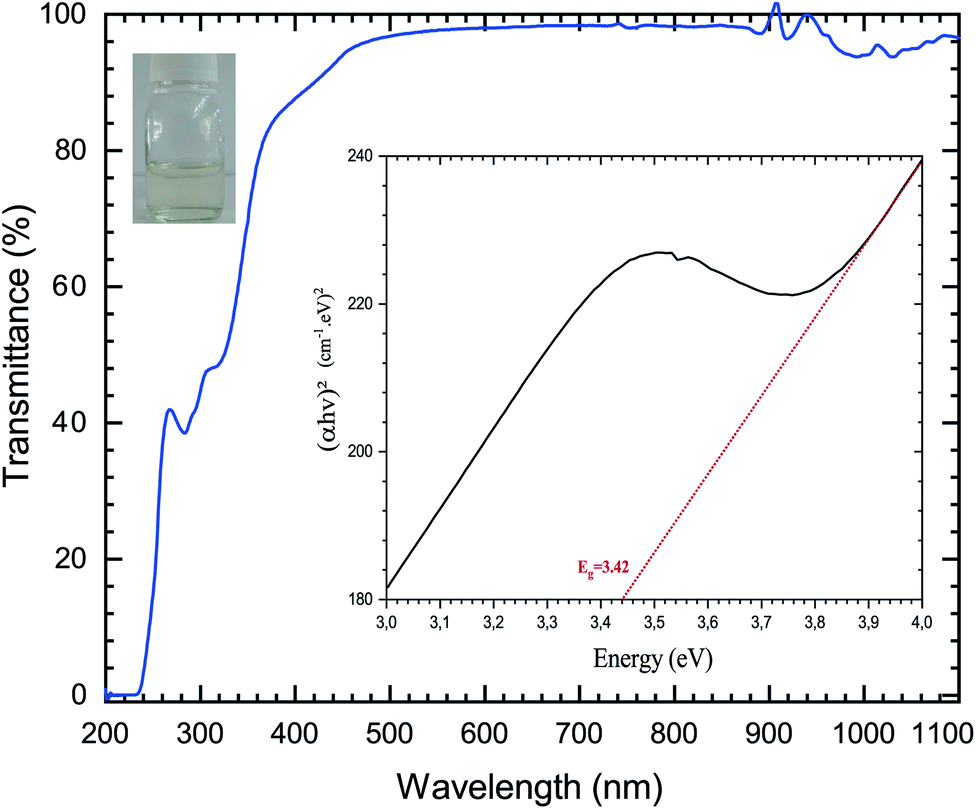 | ||
| Fig. 1 Transmittance spectra of the ZnO solution based on sol–gel methods; the inset shows the determination of the bandgap energy Eg using Tauc’s, and photographs of the ZnO aged solution. | ||
The optical band gap energy (Eg) of the ZnO sol–gel was obtained from the transmission spectra and determined from Tauc’s equation for direct band gap semiconductors using:35
|
A = αd = −lnT
| (1) |
 | (2) |
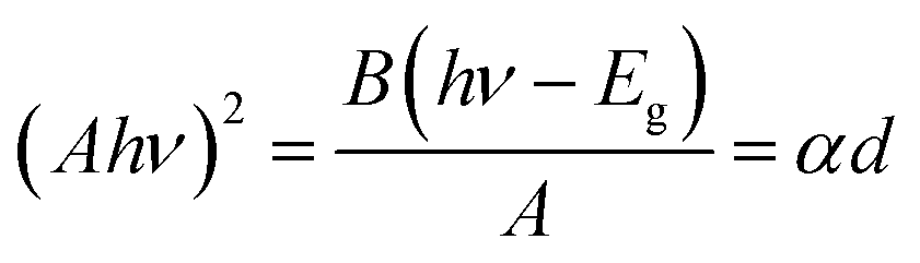
Fig. 2 shows SEM images of the ZnO sol–gel thin-films deposited on the Si substrate after pre-annealing at 300 °C with spin speeds of either 1000 rpm, 2000 rpm, or 3000 rpm for 30 s, where the thin-film thickness changes inversely with rotation rate. We see in Fig. 2, the dispersed fiber-like structures (also called skeletal branch or wrinkles) in the micro-sized scales on the sample surfaces. We observe in Fig. 2a–c, the dependence of the skeletal branch density on the spin coating rate during the pre-annealing treatment at 300 °C. This phenomenon could be avoided by increasing the spin speed and leading to an excellent degree of homogeneity. As the film thickness decreases, the fiber-like pattern disappears and the sample surface becomes smooth, while with annealing at 400 °C, we observed that the thin-film morphology is retained at all rpm speeds. As expected, at 3000 rpm the morphology of the surface is clear and the fiber patterns less defined than the other samples because of the spreading caused by the high spin rotation. Further increase in roughness with an increase in annealing temperature may be due to further grain growth as the concentration of the precursor increases.36–38 Nevertheless, the formation of these wrinkles in the ZnO sol–gel thin-films caused by stress relaxation is a phenomenon that is frequently encountered in micro- and nanotechnology. It is well known that total stress in the thin-films is commonly based on intrinsic stress and extrinsic stress:39 firstly, the intrinsic stress, is caused by impurities, defects, and lattice distortions in the crystal; secondly, the extrinsic stress, is caused by lattice mismatch and coefficient of thermal expansion mismatch between the film and the substrate. During the drying process, an inhomogeneous wrinkle pattern was distributed over the complete surface of the ZnO sol–gel thin film.33 At low temperatures (below 170 °C), the evaporation of the liquid on the sol–gel matrix is not complete. This causes at the film–air interface, an increase in the surface tension which induces residual stress. On the bottom layer, the solvent is reached from the interior of the structure to the surface by the capillary force gradient of the liquid phase which induces an increase in the volumetric strain. However, when the drying temperature increases above the boiling point, it causes the abrupt evaporation of the solvent. The differences in the expansion coefficient causes a mismatch between the film and the substrate and decrease in the capillary force of the liquid phase, resulting in compressive stress which leads to the wrinkle on the surface.40 Herein, the strain in the ZnO sol–gel thin-films is likely to be thermal – rather than intrinsic – in origin, because the linear thermal expansion coefficients (CTE or α), for the ZnO thin-film (αZnO = 6.05 × 10⁻⁶ °C−1) and the silicon substrate (αSi = 3.3 × 10⁻⁶ °C−1),41 is significantly different. Kwon et al.40 reported a theoretical basis for the wrinkle formation of ZnO sol–gel thin-films. A schematic depiction of this film wrinkling phenomenon is presented in Fig. 2d, with an SEM cross-section of the ZnO sol–gel thin-films achieved after post-annealing at 400 °C. This stress tends to be considerably more extensive in post-annealing films than in pre-annealed samples due to the high volatility of the solvent and boiling point of MEA (see Table 1). Despite its relatively high boiling point, this wrinkle formation was also achieved with an EDA stabilizer, as described in Table 1.
 | ||
| Fig. 2 SEM images of ZnO sol–gel deposited on Si after thermal annealing: (a) 1000 rpm, (b) 2000 rpm, and (c) 3000 rpm top view; and (d) samples pre-annealed at 300 °C and post-annealed at 400 °C. | ||
| Name (abbreviation) | Chemical formula | Viscosity (mPa s) | Boiling point (°C) |
|---|---|---|---|
| Triethylamine (TeA) | (CH2CH2)3–N | 0.363 | 90 |
| Ethylenediamine (EDA) | H2N–(CH2CH2) NH2 | 1.8 | 118 |
| Monoethanolamine (MEA) | (CH2CH2OH)–NH2 | 19.4 | 170 |
| Diethanolamine (DEA) | (CH2CH2OH)2–NH | 351 | 271 |
| Triethanolamine (TEA) | (CH2CH2OH)3–N | 592 | 335 |
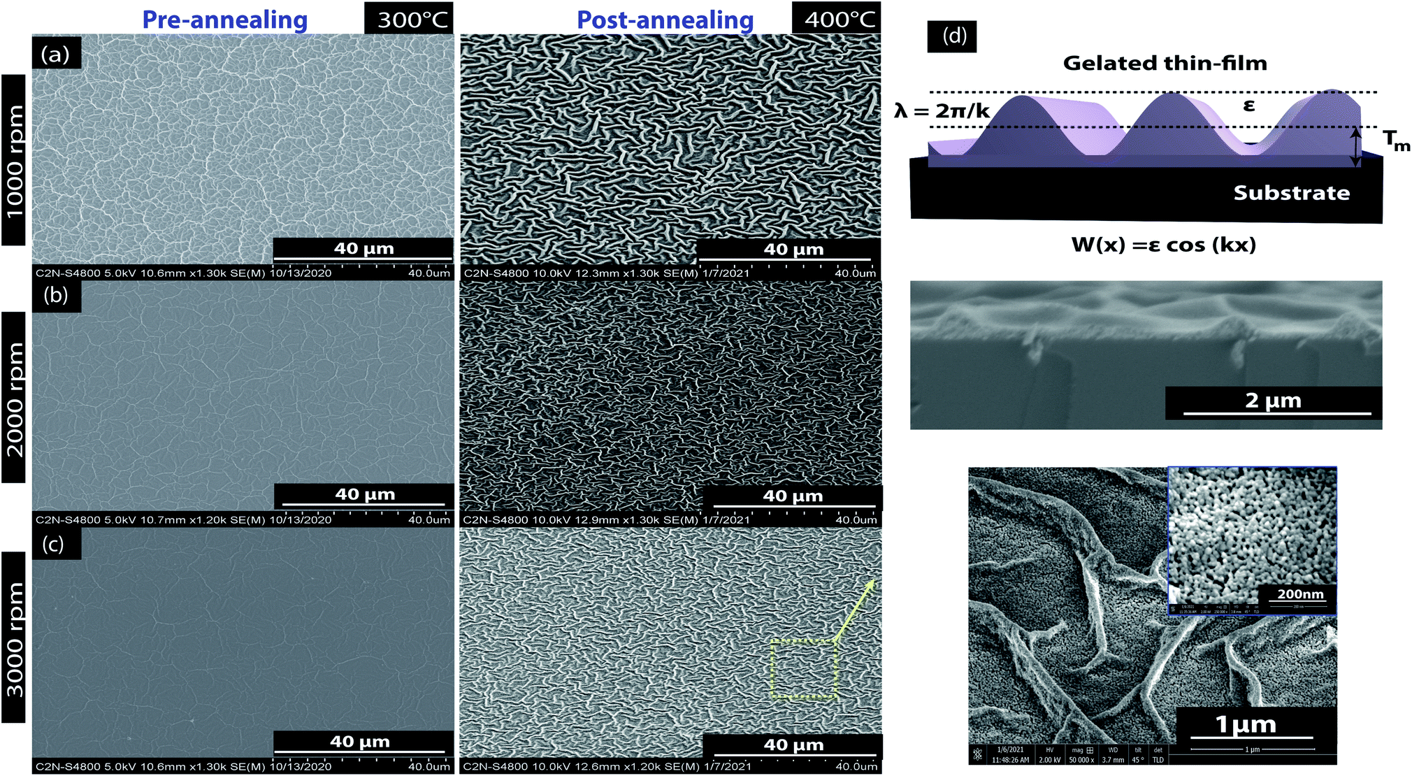
As shown in Fig. 3, the B1 modes are considered silent modes and they are inactive in Raman and infrared while A1 and E1 are both active in Raman and infrared. E2 mode is only active with Raman. And in this unit cell, there are 12 photonic modes distributed as: 6 transverse optical (TO), 3 longitudinal optical (LO), 2 transverse acoustic (TO), and 1 longitudinal acoustic (LO). Thus, the four base atoms’ motion is entirely described by these phonons in the wurtzite symmetry. For the A and B modes, the displacements are directed along the c-axis.42 For the wurtzite ZnO (space group P63mc) group theory predicts the existence of the following optic modes:43
| Γ = A1 + E1 + 2 × 10² + 2B1 | (3) |
 | ||
| Fig. 3 The identified modes of vibration of ZnO thin-films in IR and Raman spectra. | ||
The A mode model is composed of the oscillation of the rigid atom Zn vs. O atom. It causes a polarizing effect because the Zn–O bond is polar. The B1 high mode refers to the light motion of the oxygen atoms, and the B1 low mode refers to the heavier zinc sublattice motions. Accordingly, mode A is polar and mode B is not polar. The atomic displacements that are perpendicular to the c-axis are carried out in E mode. Mode E1 is provided by the two rigid sublattice oscillations, which implies that E1 exhibits oscillations of polarization. The E2 mode is related to one sublattice’s oscillation while the other one is still resting. The Elow2 mode mainly concerns the oscillation of the sublattice Zn and the Ehigh2 mode mainly concerns the O sublattice oscillation.44 So, it is important to mention that the latter modes are not polar.
Indeed, FTIR spectroscopy is a very useful tool for studying the chemical composition of ZnO sol–gel thin-films. The position of the band and the absorption peak not only depend on the chemical composition and structure of the film, but also on the morphology of the film.45 Fig. 4a shows the FTIR spectra recorded at room temperature between 400 and 4000 cm−1 of ZnO sol–gel thin-films deposited on silicon samples after annealing at 400 °C. We observe a clear and sharp peak at 422 cm−1, which corresponds to the stretching mode of the Zn–O band. The incorporation of zinc acetate in the reaction resulted in a new peak between 1570 cm−1 to 1470.21 cm−1, which was attributed to the carbonyl group of the acetate group (C![[double bond, length as m-dash]](https://www.rsc.org/images/entities/char_e001.gif) O).46 These results corroborate the Raman data. The existence of a band assigned to C–H, C–O, and C–C on the FTIR spectrum seems to indicate the residual carbon content for the sample annealed at 400 °C. This information proves that the organic substances from the precursor solution did not evaporate fully. It is well know that the sol–gel process involves the preparation of organic compounds which are considered a source of carbon. The carbon acts as an unintentional dopant during the growth process. The carbon may be substituted on the zinc side or oxygen side to form a carbon–oxygen complex defect.47 Indeed, the impact of residual carbon on an optical background cannot be ruled out.48
O).46 These results corroborate the Raman data. The existence of a band assigned to C–H, C–O, and C–C on the FTIR spectrum seems to indicate the residual carbon content for the sample annealed at 400 °C. This information proves that the organic substances from the precursor solution did not evaporate fully. It is well know that the sol–gel process involves the preparation of organic compounds which are considered a source of carbon. The carbon acts as an unintentional dopant during the growth process. The carbon may be substituted on the zinc side or oxygen side to form a carbon–oxygen complex defect.47 Indeed, the impact of residual carbon on an optical background cannot be ruled out.48
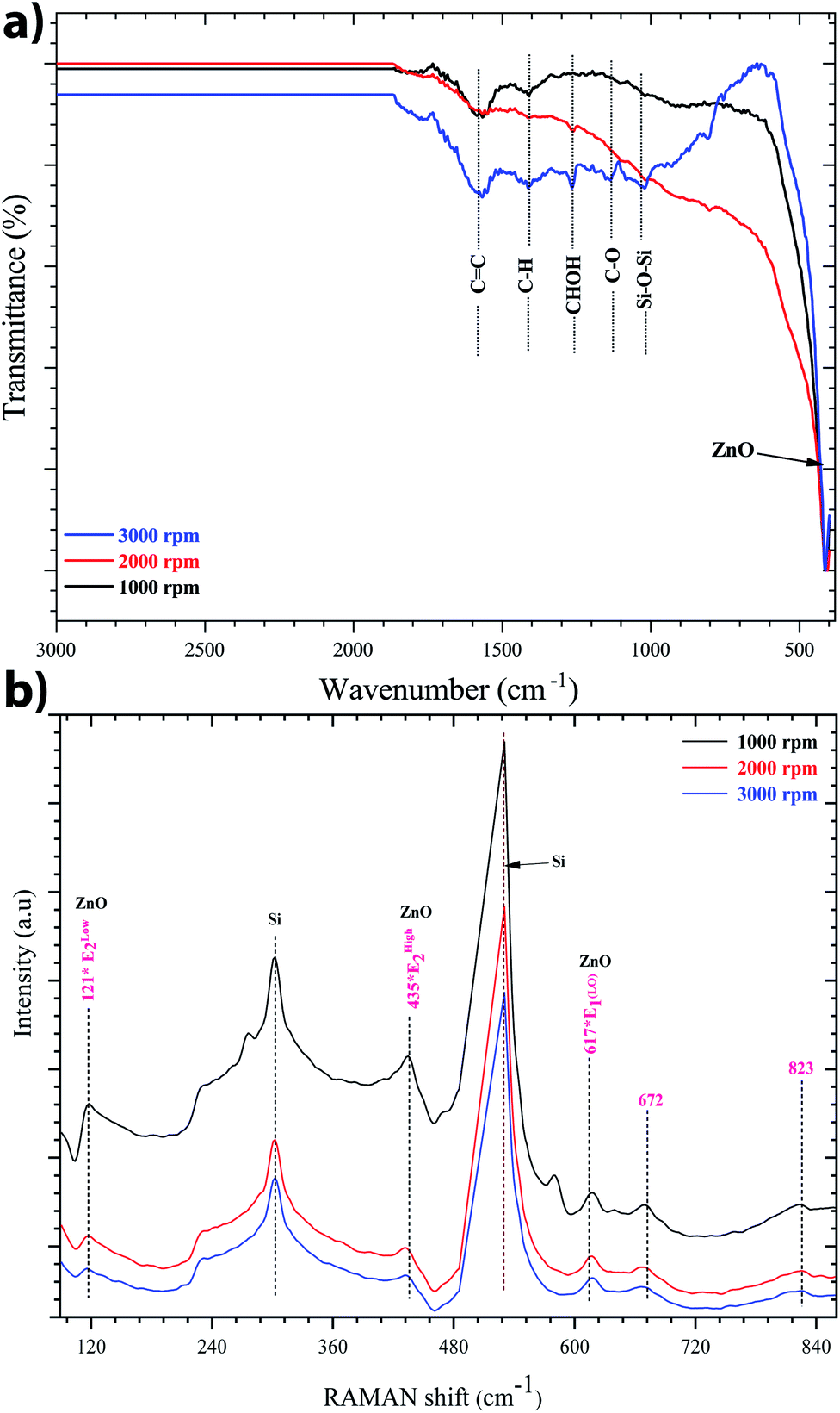 | ||
| Fig. 4 (a) FTIR spectra, and (b) Raman spectra of the sol–gel ZnO thin-film on the silicon substrate. The identified modes of vibration indicates the formation of the sol–gel ZnO structure. | ||
Fig. 4b shows the Raman spectra of the ZnO sol–gel thin-films on the silicon substrate at room temperature with different speeds of spin-coating: 1000, 2000, or 3000 rpm. This spectrum was made just after the pre-annealing, that is to say the material is not completely crystallized, so it is normal to see less intense peaks and other peaks related to the substrate or the precursor. We obtained two modes, A1(LO) and E1(LO), which occur approximately at the frequencies of 540 cm−1 and 600 cm−1, respectively. This result related to the macroscopic electrical field produced by the relative displacement inside the primitive cell, of oppositely charged atoms and therefore concerns only LO phonons, and for ZnO, there are only two LO modes, the A1(LO) and the E1(LO). We observed almost the same shape as the spectra of the pre-annealed samples but the peaks were more intense due to the crystallization of ZnO. And also we notice that when we increase the speed of spin the intensity of the Raman peaks are more intense and we can explain that by the increase of the thickness of the layers. The Elow2, Ehigh2, and A1(LO) eigenmodes of our samples are located at 121 cm−1, 435 cm−1, and 534 cm−1, respectively. Peaks at 227 cm−1, 672 cm−1, 823 cm−1 are respectively attributed to the 2 TA, 2Elow2, Ehigh2 − Elow2, and the LA + TO, and A1(TO) + Ehigh2 modes appeared as E2 in a multiphonon mode. Thus, the most prominent second-order frequencies occur as contributions of A1, E1, and E2.49 The peaks at 617 cm−1 show fundamental Raman modes.
3.2 Effect of multilayers of ZnO sol–gel on 〈100〉-silicon
To better understand the impact of the number of thin layers deposited on Si samples we demonstrated that the surface quality of ZnO thin-films increased as the spinning speed increased during the first deposition layer. This optimized spin speed was fixed at 3000 rpm for 30 s. The number of coating layers varies from 1 to 6. Each deposited thin layer of ZnO sol–gel was preheated on a hot plate at 300 °C for 15 min to evaporate the organic elements and then cooled to room temperature, next the coating was deposited. The targeted final thickness of films was annealing at 400 °C in N2 for three hours.Reflectance spectra of the ZnO sol–gel thin-films, which were recorded in the wavelength range of 200–900 nm, are shown in Fig. 5a. We observed that for multilayer deposition of ZnO sol–gel, reflection is reduced – for one layer, the reflection was less than 16% but for six layers it was 9%, which indicates the effects of ZnO anti-reflection coating layers. The effect of thickness was clearly visible in the reflection spectra. This effect is explained by the pronounced interference fringes that will be generated at a lower thickness, represented by the variance of the values of the latter, depending on the wavelength.50,51 We conclude that the reflectance was found to be higher for one layer as compared to multilayer thin-films.
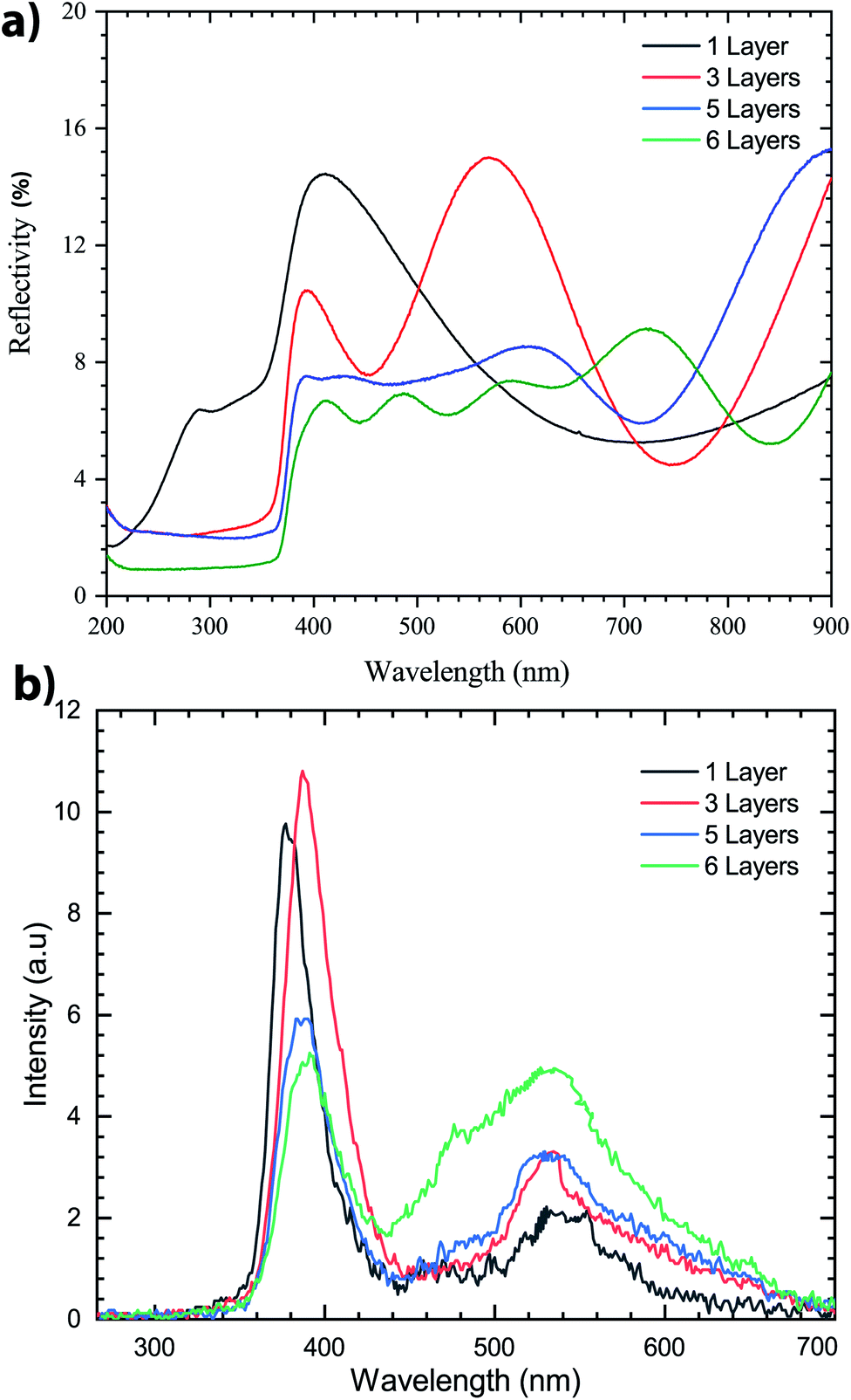 | ||
| Fig. 5 (a) Reflectivity, and (b) photoluminescence of ZnO sol–gel annealing at 400 °C in N2. | ||
Photoluminescence (PL) was measured at room temperature. As shown in Fig. 5b, after annealing of the samples, two emission peaks are found in the PL spectrum. The emission peak associated with UV excitons is shifted to higher energy. A weak and large peak centered in the 500–600 nm region is also observed in the PL spectrum. This emission peak is related to the amount of non-stoichiometric inherent defects that could be due to the zinc vacancy in ZnO thin-films.29 It is clear that there is a significant increase of PL peak intensity in the UV emission for three layers, compared with the other samples which indicates that exciton recombination was high for this sample. However, the excitonic peak position is blueshifted for the sample with three layers, then decreases for samples with five and six layers, which could be associated with the compressive strain generated by wrinkles. Indeed, this peak moved toward lower energy for samples with five and six layers which could be associated with tensile strain generation.52 These findings tend to be due to the increased crystallinity of the thicker layer, and can be attributed to reducing the size of the ZnO grain or the existence of compressed stress.
3.3 Structural characterization of ZnO thin-films
ZnO has been recognized as a thin-film piezoelectric material. Among the piezoelectric films reported, some investigations have achieved manufacturing and applications, especially for ZnO and AlN.53 The latter has the advantage that it can be deposited on Si, the most important semiconductor and compatible with industrial manufacturing. It is well-known that the c-axis orientation is one of the necessary conditions for thin-films to be piezoelectric.41 In addition, the degree of orientation of the c-axis for ZnO thin-films has been reported to be strongly dependent on the initial concentration in solution. This is supported by Malek et al.,38 who have shown that the peaks for the ZnO sol–gel thin-films prepared using the 0.2 M solution are weaker compared to other films with the concentration range from 0.4 M to 1 M. These results indicate that the ZnO sol–gel thin-film growth from the 0.2 M solution was not strong due to insufficient amounts of the zinc species in solution, which has slowed the growth of ZnO thin-films compared to thin-films grown at higher concentrations.The XRD patterns presented in Fig. 6 indicate all the polycrystalline ZnO thin-films from the 0.75 M solution, with a structure that belongs to the hexagonal wurtzite structures of ZnO.54 Fig. 6 shows the X-ray diffraction (XRD) spectra of the ZnO sol–gel thin-films on silicon samples, with various thickness after annealing at 400 °C under a N2 or air atmosphere. ZnO crystallizes at atmospheric pressure and temperature in the wurtzite structure, which is a hexagonal network characterized by two interpenetrating sub-networks of Zn2+ and O2− ions, such that each Zn ion is surrounded by a tetrahedron of oxygen ions and vice versa. This arrangement results in polar symmetry along the hexagonal longitudinal axis (c axis). Beyond two layers deposited by spin coating, we have grown crystallites along the different directions (100), (101), (103) and (002). The diffraction peak along the (002) plane corresponds to typical hexagonal wurtzite. The measured thicknesses by cross-sectional SEM images confirm the XRD results. The increasing intensity of all diffraction peaks is influenced by the thickness of the ZnO sol–gel thin-films.
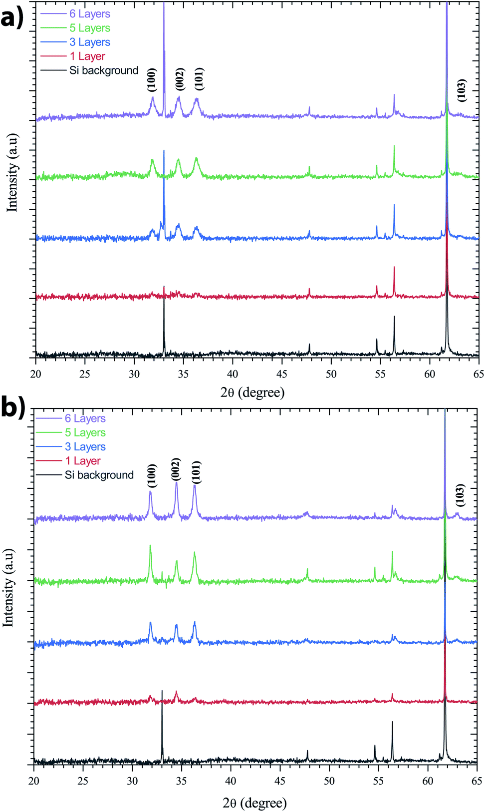 | ||
| Fig. 6 XRD spectra of the ZnO-sol–gel annealing at 400 °C with different thickness (a) under N2, and (b) under an air atmosphere. | ||
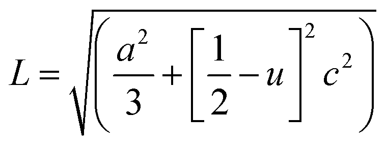
The Zn–O bond length L is given by:55
 | (4) |
 | (5) |
 | (6) |
 | (7) |
| Layer | Thickness (nm) | ρ (Ω cm) | 2θ | FWHM | D (nm) | a (Å) | c (Å) | a/c | L (Å) | σ (GPa) | |
|---|---|---|---|---|---|---|---|---|---|---|---|
| N2 | 1 layer | 95 | 0.065 | 34.43 | 0.64 | 13.2 | 3.24 | 5.21 | 0.62 | 2.60 | −2.09 |
| 3 layers | 120 | 0.21 | 34.43 | 0.42 | 16.9 | 3.24 | 5.21 | 0.62 | 2.60 | −1.37 | |
| 5 layers | 420 | 0.3 | 34.43 | 0.5 | 16.9 | 3.24 | 5.21 | 0.62 | 2.60 | −1.54 | |
| 6 layers | 600 | 0.33 | 34.46 | 0.34 | 29.5 | 3.24 | 5.20 | 0.62 | 2.60 | −0.94 | |
| Air | 1 layer | 95 | 0.051 | 34.44 | 0.31 | 27.3 | 3.24 | 5.21 | 0.62 | 2.60 | −1.02 |
| 3 layers | 120 | 0.149 | 34.44 | 0.23 | 48.4 | 3.24 | 5.21 | 0.62 | 2.60 | −0.58 | |
| 5 layers | 420 | 0.267 | 34.45 | 0.23 | 35.9 | 3.24 | 5.20 | 0.62 | 2.60 | −0.75 | |
| 6 layers | 600 | 0.31 | 34.44 | 0.23 | 35.8 | 3.24 | 5.21 | 0.62 | 2.60 | −0.75 |
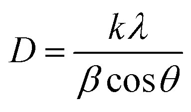
The mean crystallite size (D) was evaluated according to broadening of the highest intensity peak corresponding to the (002) diffraction plane using the Debye–Scherrer formula shown in eqn 8:57
 | (8) |
As observed in Table 2, we obtained larger D (ranging from 27.3 nm to 35.9 nm) and smaller FWHM values for ZnO sol–gel thin-films annealing in air than thin-films annealing in N2 conditions. These results indicate the better crystallization of the ZnO sol–gel thin-films annealing in air.
The preferential crystal orientation can be analyzed from the texture coefficient (TC) given by:58
 | (9) |
In Fig. 7, it was observed that the highest TC(hkl) was in the (002) plane for all the films. Nevertheless, all TC values vary as a function of the number of layers, whatever the annealing conditions under N2 or in air.
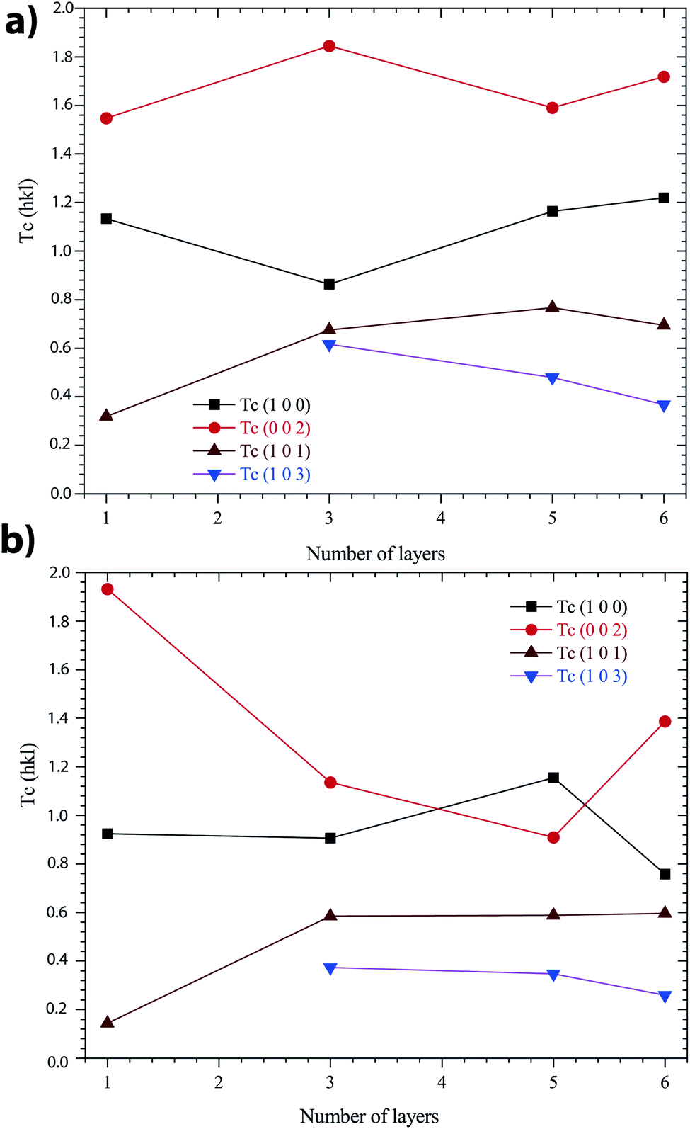 | ||
| Fig. 7 Variation of TC(hkl) values of the ZnO sol–gel thin-films with a different number of layers: (a) annealing in N2, and (b) annealing in air. | ||
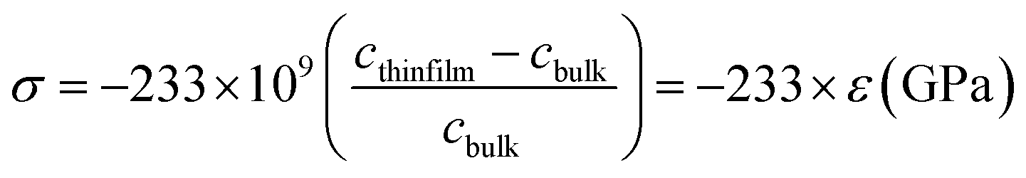
The strain (ε) and stress (σ) in the thin-films, along the c-axis, which are calculated using the equations as shown below:
 | (10) |
 | (11) |
Compressive strain range from −0.58 GPa to −2.09 GPa was observed at 400 °C, as presented in Table 2. As we increased the number of layers, the compressive strain becomes weaker. The compressive strain obtained in the ZnO sol–gel thin-films is likely to be intrinsic stress, rather than thermal stress, in origin. It indicates that the thin-films having lower compressive stress leading to a weaker FWHM of 0.18 for −0.58 GPa, as compared to the thin-films having higher compressive stress with FWHM of 0.64 for −2.09 GPa.
4 Discussion
In the sol–gel spin coating process, the ZnO thin film characteristics were affected by the solvent, chemical solutions, annealing conditions, and film thickness.58–60 Only MEA was used because the polarity, reactivity, boiling point, and viscosity parameters affected the sol–gel behavior and thin-film properties. The choice of amine is based on its good miscibility with alcohol solvent and the high boiling point, which allows it to have a solution with a low evaporation rate (low volatility) at room temperature during soil preparation (see Table 1). The MEA and TeA have strong polarity and basicity compared to DEA, TEA, and EDA. These properties induce the formation of the tetrahedral-shaped complexes and contribute to the highly c-axis orientated thin films in DRX pattern. On the other hand, stabilized TEA and TeA are not fully transparent compared to other sol–gels. Thus, we used MEA, which is the most stable and consistently maintains transparency and homogeneity during the process compared to the other amine compounds. The roughness of film depends on the substrate roughness, but it also varies based on film thickness. The first important thing to be considered in the spin coating is uniform solution preparation. Aryanto et al.15 reported that the ZnO grain size decreases, while the thin film thickness increases as a result of increasing precursor concentration from 0.3 to 1 M. This work showed that the morphology and structure of ZnO sol–gel thin-films prepared using sol–gel methods, with a concentration of 0.75 M, were influenced by spin-coating and multistack layers. Herein, we point out that the surface morphology analyzed by the SEM micrograph of ZnO thin-films is important. We can obtain the same fiber-like structure as observed by Khan et al.,61 where the ZnO sol–gel synthesized with the molar ratio of monoethanolamine to zinc acetate was held at 1.0 and the zinc acetate concentration at 0.80 mol L−1.The SEM results were used to verify the optimum spin coating parameters necessary to achieve the specified thickness of the film coating and surface roughness for quality ZnO sol–gel thin-film. We observe that the surface quality increased with an increase in speed from 1000 to 3000 rpm. Shivaraj et al. reported that the risk of the highest spinning speed (above 3000 rpm) could increase the surface roughness, while the reasonable spinning speed will achieve the smoothest surface.60 Thus, the thin film processed in the present work, is a good quality surface, and uniformity was obtained at 3000 rpm. Shelke et al. reported that post-annealing decreases the thickness of ZnO thin films.54 This change in thickness is attributed to an increase in thin film density at higher temperatures. After dicing the samples, the average thicknesses of the thin-films measured range from 100 and 600 nm. As expected, the higher spinning speed decreases the thin-film thickness. We observed that the root-mean-square (RMS) roughness seems to increase as the thin-film thickness increases in the range from 14 nm to 400 nm. Nevertheless, it was difficult to give the average value of RMS due to the presence of an inhomogeneous wrinkle pattern distributed over the complete surface of the ZnO sol–gel thin films.
The choice of solvents used also affects the crystal orientation of the deposited ZnO sol–gel thin-films. Fig. 8 shows the effect of the isopropyl alcohol on the crystal orientation of the deposited thin-films on Si samples. It is well known that the FWHM values of ZnO thin-films decrease with increasing temperature up to 800 °C.55 Herein, we point out that the combination of isopropyl alcohol and annealing treatment in air seems to be the best strategy to obtain preferentially (002) c-oriented ZnO sol–gel thin-films with lower FWHM.
 | ||
| Fig. 8 XRD patterns of different ZnO sol–gel thin-film thicknesses annealed in air at 400 °C, using isopropyl alcohol as the solvent. | ||
Compared to thin-film annealing in air using ethanol as a solvent, the values a, c, L, D, and FWHM, in ZnO sol–gel thin-films are not affected by the use of isopropyl alcohol.
However, annealing in an air environment allows oxygen to diffuse from air into the structure of the ZnO thin-films. Firstly, the uncoordinated zinc sites on the surface react with oxygen atoms in air, then oxygen ions diffuse into the crystal structure to oxygen-deficient regions. Also, the carbon residual contained on the ZnO surface will react with oxygen during annealing to be converted to COx and escape from the surface, resulting in a decrease in the amount of residue carbon. But, during nitrogen annealing, the low conversion effect occurs at the surface leading to an increase in oxygen vacancies which may induce stress in the lattice structure. The higher surface roughness of the sample annealed in air compared to the sample annealed in nitrogen was attributed to the increasing grain size. As the surface roughness increases, it seems to adsorb oxygen on the surface of the crystallites. The annealing at high temperatures in air tends to improve the surface and crystallinity of the thin films.
In order to provide electric properties, thin-films resistance was evaluated using a four-point probe technique that is commonly used in the semiconductor industry.62 This approach removes measurement errors due to the contact resistance between the probe and the sample, which typically occur in the two-point probe measurement technique. The resistivity and conductivity of ZnO sol–gel thin-films were determined by:63
 | (12) |
These complementary measurement results are presented in Fig. 9, in order to obtain the electrical resistivity (ρ), as summarized in Table 2. We obtained a resistivity of ZnO sol–gel thin-films annealing at 400 °C, ranging from 0.05 Ω.cm to 0.33 Ω.cm. The variations in electrical properties, such as conductivity of ZnO thin-films annealing in N2, occurred by oxygen vacancy, shallow interstitial zinc, and other donor-type point defects. The resistivity was found to decrease with insufficient thickness. As a result, the increase in thickness due to more coating cycles reduces the conductivity of ZnO sol–gel thin-films. These results are in good agreement with the results of XRD. We have observed that the crystallinity of thin-films improves with the number of coating layers, resulting in a decrease in the conductivity.54
 | ||
| Fig. 9 I–V characteristics of ZnO thin-films annealed in air at 400 °C. | ||
In cases where we can integrate devices based on standard CMOS technologies, the only compatibility issue might be the requirement for additional steps in the process. These issues can include mechanical stress, chemical contamination, selectivity, or the need for high temperatures during processing. In some manufacturing technologies, this has led to alternative hybrid technology (also called heterogeneous integration), where the materials or components are on separate chips, and then combined in a single packaging.64,65 However, the thin film high-temperature growth prevents direct growth on CMOS chips, and the transfer process adds extra cost to the final product. The post-annealing treatment of ZnO sol–gel thin-films can vary between 250 °C to 900 °C based on the substrates used. Herein, our strategy was to keep the thermal budget at 400 °C in order to ensure the compatibility of CMOS and thereby provide the advantages of ZnO thin-film properties (direct band-gap, piezoelectricity, and so on) in flexible,9 monolithic and heterogeneous technology. ZnO is similar to GaN,66,67 which is commonly used in high-performance optoelectronic devices, making the latter a promising candidate material for advanced device applications which could revolutionize the field of hybrid photonic/electronic devices.17,65 Good PL results and enhancement in the crystallinity were well supported by XRD and electrical measurement results. Our results are the basis for future studies of green sensors intended for harsh environments and produced at low cost.
5 Conclusions
Structural, morphological, optical, and electrical characteristics of ZnO thin-films developed by the sol–gel spin coating method on (100) Si samples have been investigated in the present work. XRD diffraction showed that the crystalline nature of the ZnO thin-films increased with the thickness of the layers. The peaks were indexed to (100), (101), and (002) planes. The amplitude of all diffraction peaks increased and increased in the full width half-maximum (FWHM) value with increasing thickness layer. The c-axis orientation improved, and the grain size increased, as indicated by the increased intensity of the (002) plane peak at 2θ = 34°, corresponding to hexagonal ZnO crystals. Furthermore, we consider that the deposited ZnO sol–gel thin-film piezoelectrical properties also give good results for piezo-devices. Studies on this matter will be done in the future.Conflicts of interest
There are no conflicts to declare.Acknowledgements
The authors acknowledge the cleanroom and characterization laboratory staff of C2N and CRTEn. We also acknowledge D. Bouville, C. Dupuis, F. Maillard, and A. Durnez, for valuable advice. This work was partly supported by the French RENATECH network with technological facilities. Experimental work was supported by French grants ANR Deus-nano (ANR-19-CE42-0005).Notes and references
- A. P. Bhirud, S. D. Sathaye, R. P. Waichal, L. K. Nikam and B. B. Kale, Green Chem., 2012, 14, 2790–2798 RSC.
- S. Iravani, Green Chem., 2011, 13, 2638–2650 RSC.
- B. Bahramian, Y. Ma, R. Rohanizadeh, W. Chrzanowski and F. Dehghani, Green Chem., 2016, 18, 3740–3748 RSC.
- M. Tanaka, K. Sato, E. Kitakami, S. Kobayashi, T. Hoshiba and K. Fukushima, Polym. J., 2015, 47, 114–121 CrossRef CAS.
- K. Guerchouche, E. Herth, L. E. Calvet, N. Roland and C. Loyez, Microelectron. Eng., 2017, 182, 46–52 CrossRef CAS.
- Y. Cao and K. E. Uhrich, J. Bioact. Compat. Polym., 2019, 34, 3–15 CrossRef CAS.
- V. Saunier, E. Flahaut, M.-C. Blatché, C. Bergaud and A. Maziz, Biosens. Bioelectron., 2020, 165, 112413 CrossRef CAS PubMed.
- D. M. Cruz, E. Mostafavi, A. Vernet-Crua, H. Barabadi, V. Shah, J. L. Cholula-Díaz, G. Guisbiers and T. J. Webster, JPhys Mater., 2020, 3, 034005 CrossRef CAS.
- E. Herth, K. Guerchouche, L. Rousseau, L. E. Calvet and C. Loyez, Microsyst. Technol., 2017, 23, 5921–5929 CrossRef CAS.
- V. A. Coleman and C. Jagadish, in Zinc Oxide Bulk, Thin Films and Nanostructures, ed. C. Jagadish and S. Pearton, Elsevier Science Ltd, Oxford, 2006, pp. 1–20 Search PubMed.
- O. Lupan, G. A. Emelchenko, V. V. Ursaki, G. Chai, A. N. Redkin, A. N. Gruzintsev, I. M. Tiginyanu, L. Chow, L. K. Ono, B. Roldan Cuenya, H. Heinrich and E. E. Yakimov, Mater. Res. Bull., 2010, 45, 1026–1032 CrossRef CAS.
- N. Amara, A. Martin, A. Potdevin, D. Riassetto, M. Messaoud, F. Réveret, G. Chadeyron, J. Bouaziz and M. Langlet, J. Alloys Compd., 2020, 842, 155708 CrossRef CAS.
- O. Jamadi, F. Reveret, P. Disseix, F. Medard, J. Leymarie, A. Moreau, D. Solnyshkov, C. Deparis, M. Leroux, E. Cambril, S. Bouchoule, J. Zuniga-Perez and G. Malpuech, Light: Sci. Appl., 2018, 7, 82 CrossRef CAS PubMed.
- M. F. Khan, A. H. Ansari, M. Hameedullah, E. Ahmad, F. M. Husain, Q. Zia, U. Baig, M. R. Zaheer, M. M. Alam, A. M. Khan, Z. A. AlOthman, I. Ahmad, G. M. Ashraf and G. Aliev, Sci. Rep., 2016, 6, 27689 CrossRef CAS PubMed.
- D. Aryanto, W. Jannah, S. T. Masturi, A. Wismogroho, P. Sebayang and M. P. Sugianto, J. Phys.: Conf. Ser., 2017, 817(1), 012025 CrossRef.
- G. Guisbiers and S. Pereira, Nanotechnology, 2007, 18, 435710 CrossRef.
- F. Tabataba-Vakili, C. Brimont, B. Alloing, B. Damilano, L. Doyennette, T. Guillet, M. El Kurdi, S. Chenot, V. Brändli and E. Frayssinet, et al., Appl. Phys. Lett., 2020, 117, 121103 CrossRef CAS.
- S. K. Arya, S. Saha, J. E. Ramirez-Vick, V. Gupta, S. Bhansali and S. P. Singh, Anal. Chim. Acta, 2012, 737, 1–21 CrossRef CAS PubMed.
- D. Coutancier, S.-T. Zhang, S. Bernardini, O. Fournier, T. Mathieu-Pennober, F. Donsanti, M. Tchernycheva, M. Foldyna and N. Schneider, ACS Appl. Mater. Interfaces, 2020, 12, 21036–21044 CrossRef CAS PubMed.
- S. Margueron, S. Ropers, A. Maertens, O. Legrani, F. Genty, A. Bartasyte and T. Belmonte, Mater. Chem. Phys., 2014, 147, 623–628 CrossRef CAS.
- D. Taïnoff, M. Al-Khalfioui, C. Deparis, B. Vinter, M. Teisseire, C. Morhain and J.-M. Chauveau, Appl. Phys. Lett., 2011, 98, 131915 CrossRef.
- J. Sun, D. A. Mourey, D. Zhao and T. N. Jackson, J. Electron. Mater., 2008, 37, 755–759 CrossRef CAS.
- O. Legrani, O. Elmazria, S. Zhgoon, P. Pigeat and A. Bartasyte, IEEE Sens. J., 2013, 13, 487–491 CAS.
- T. Nurtono, T. C. Kusuma, M. Hudandini, W. Widiyastuti, M. Shimada, S. Madhania, S. Machmudah, D. Puspitasari, S. Winardi and K. Kusdianto, AIP Conf. Proc., 2020, 2220, 030005 CrossRef.
- R. A. Zargar, P. A. Ahmad, M. A. S. Gogre and M. M. Hassan, Opt. Quantum Electron., 2020, 52, 401 CrossRef CAS.
- S. Temel, F. O. Gokmen and E. Yaman, Bull. Mater. Sci., 2020, 43, 18 CrossRef CAS.
- M. Li, J. Zhai, H. Liu, Y. Song, L. Jiang and D. Zhu, J. Phys. Chem. B, 2003, 107, 9954–9957 CrossRef CAS.
- L. L. Hench and J. K. West, Chem. Rev., 1990, 90, 33–72 CrossRef CAS.
- H. Li, J. Wang, H. Liu, H. Zhang and X. Li, J. Cryst. Growth, 2005, 275, e943–e946 CrossRef CAS.
- C.-Y. Tsay, K.-S. Fan, S.-H. Chen and C.-H. Tsai, J. Alloys Compd., 2010, 495, 126–130 CrossRef CAS.
- D. Visser, Z. Ye, C. Prajapati, N. Bhat and S. Anand, ECS J. Solid State Sci. Technol., 2017, 6, P653 CrossRef CAS.
- L. S. Karimi, S. Amiri and M. H. Zori, Silicon, 2020, 13, 2195–2207 CrossRef.
- P. Hosseini Vajargah, H. Abdizadeh, R. Ebrahimifard and M. Golobostanfard, Appl. Surf. Sci., 2013, 285, 732–743 CrossRef CAS.
- M. Wang, J. Wang, W. Chen, Y. Cui and L. Wang, Mater. Chem. Phys., 2006, 97, 219–225 CrossRef CAS.
- J. Tauc, R. Grigorovici and A. Vancu, Phys. Status Solidi B, 1966, 15, 627–637 CrossRef CAS.
- V. Kumar, N. Singh, R. Mehra, A. Kapoor, L. Purohit and H. Swart, Thin Solid Films, 2013, 539, 161–165 CrossRef CAS.
- R. Kumar, N. Khare, V. Kumar and G. Bhalla, Appl. Surf. Sci., 2008, 254, 6509–6513 CrossRef CAS.
- M. F. Malek, M. H. Mamat, M. Z. Sahdan, M. M. Zahidi, Z. Khusaimi and M. R. Mahmood, Thin Solid Films, 2013, 527, 102–109 CrossRef CAS.
- E. Herth, D. Fall, J.-Y. Rauch, V. Mourtalier and G. Guisbiers, J. Mater. Sci.: Mater. Electron., 2020, 31, 4473–4478 CrossRef CAS.
- S. J. Kwon, J.-H. Park and J.-G. Park, Phys. Rev. E, 2005, 71, 011604 CrossRef PubMed.
- E. Herth, E. Algré, J.-Y. Rauch, J.-C. Gerbedoen, N. Defrance and P. Delobelle, Phys. Status Solidi A, 2016, 213, 114–121 CrossRef CAS.
- Y. Song, S. Zhang, C. Zhang, Y. Yang and K. Lv, Crystals, 2019, 9, 395 CrossRef CAS.
- R. Cuscó, E. Alarcón-Lladó, J. Ibanez, L. Artús, J. Jiménez, B. Wang and M. J. Callahan, Phys. Rev. B, 2007, 75, 165202 CrossRef.
- S. K. Sharma and G. J. Exarhos, Raman Spectroscopic Investigation of ZnO and Doped ZnO Films, Nanoparticles and Bulk Material at Ambient and High Pressures, Conference Name: Semiconductor Materials and Technology (ICSMT), ISBN: 9783908450252 ISSN: 1662-9779, Publisher: Trans Tech Publications Ltd, 1997, vol. 55, pp. 32–37 Search PubMed.
- Z. Yang, Z. Ye, Z. Xu and B. zhao, Phys. E, 2009, 42, 116–119 CrossRef CAS.
- B. Arik and O. D. Karaman Atmaca, Cellulose, 2020, 27, 8385–8403 CrossRef CAS.
- S. T. Tan, X. W. Sun, Z. G. Yu, P. Wu, G. Q. Lo and D. L. Kwong, Appl. Phys. Lett., 2007, 91, 072101 CrossRef.
- E. Nowak, M. Szybowicz, A. Stachowiak, W. Koczorowski, D. Schulz, K. Paprocki, K. Fabisiak and S. Los, Appl. Phys. A: Mater. Sci. Process., 2020, 126, 552 CrossRef CAS.
- I. Musa, N. Qamhieh and S. T. Mahmoud, Results Phys., 2017, 7, 3552–3556 CrossRef.
- M. A. Zubair, M. T. Chowdhury, M. S. Bashar, M. A. Sami and M. F. Islam, AIP Adv., 2019, 9, 045123 CrossRef.
- T. Gungor, E. Gungor and B. Saka, Nanomater. Nanotechnol., 2016, 6, 1847980416673785 Search PubMed.
- F. Fang, D. Zhao, B. Li, Z. Zhang, D. Shen and X. Wang, J. Phys. Chem. C, 2010, 114, 12477–12480 CrossRef CAS.
- E. Herth, L. Valbin, F. Lardet-Vieudrin and E. Algré, Microsyst. Technol., 2017, 23, 3873–3880 CrossRef CAS.
- V. Shelke, M. Bhole and D. Patil, Mater. Chem. Phys., 2013, 141, 81–88 CrossRef CAS.
- S. Aksoy, Y. Caglar, S. Ilican and M. Caglar, European Conference of Chemical Engineering, ECCE'10, European Conference of Civil Engineering, ECCIE'10, European Conference of Mechanical Engineering, ECME'10, European Conference of Control, ECC'10, 2010, pp. 227–231 Search PubMed.
- B. D. Cullity, Am. J. Phys., 1957, 25, 394–395 CrossRef.
- S. Maniv and A. Zangvil, J. Appl. Phys., 1978, 49, 2787–2792 CrossRef CAS.
- S. Ilican, Y. Caglar and M. Caglar, J. Optoelectron. Adv. Mater., 2008, 10, 2578–2583 CAS.
- A. Gahtar, A. Rahal, B. Benhaoua and S. Benramache, Optik, 2014, 125, 3674–3678 CrossRef CAS.
- B. Shivaraj, H. N. Murthy, M. Krishna and S. Sharma, International Journal of Thin Film Science and Technology, 2013, 2, 143–154 CrossRef.
- Z. R. Khan, M. S. Khan, M. Zulfequar and M. S. Khan, Mater. Sci. Appl., 2011, 5, 4 Search PubMed.
- K. Shimanovich, Y. Bouhadana, D. A. Keller, S. Rühle, A. Y. Anderson and A. Zaban, Rev. Sci. Instrum., 2014, 85, 055103 CrossRef PubMed.
- L. I. Maissel, R. Glang and P. P. Budenstein, J. Electrochem. Soc., 1971, 118, 114C CrossRef.
- A. Elbaz, R. Arefin, E. Sakat, B. Wang, E. Herth, G. Patriarche, A. Foti, R. Ossikovski, S. Sauvage, X. Checoury, K. Pantzas, I. Sagnes, J. Chrétien, L. Casiez, M. Bertrand, V. Calvo, N. Pauc, A. Chelnokov, P. Boucaud, F. Boeuf, V. Reboud, J.-M. Hartmann and M. El Kurdi, ACS Photonics, 2020, 7, 2713–2722 CrossRef CAS.
- G. Duan, C. Jany, A. Le Liepvre, M. Lamponi, A. Accard, F. Poingt, D. Make, F. Lelarge, S. Messaoudene, D. Bordel, J. Fedeli, S. Keyvaninia, G. Roelkens, D. Van Thourhout, D. J. Thomson, F. Y. Gardes and G. T. Reed, 2012 International Conference on Indium Phosphide and Related Materials, 2012, pp. 16–19 Search PubMed.
- Ü. Özgür, Y. I. Alivov, C. Liu, A. Teke, M. Reshchikov, S. Doğan, V. Avrutin, S.-J. Cho and H. Morkoç and, J. Appl. Phys., 2005, 98, 11 CrossRef.
- J. Zuniga-Perez, E. Mallet, R. Hahe, M. J. Rashid, S. Bouchoule, C. Brimont, P. Disseix, J. Y. Duboz, G. Gommé, T. Guillet, O. Jamadi, X. Lafosse, M. Leroux, J. Leymarie, F. Li, F. Réveret and F. Semond, Appl. Phys. Lett., 2014, 104, 241113 CrossRef.
| This journal is © The Royal Society of Chemistry 2021 |