
 Open Access Article
 This Open Access Article is licensed under a
 Creative Commons Attribution 3.0 Unported Licence
Electronic and optical properties of silicene on GaAs(111) with hydrogen intercalation: a first-principles study
Ting Yu,
He Zhang,
Dan Li and
Yanwu Lu*
and
Yanwu Lu*
Department of Physics, School of Science, Beijing Jiaotong University, Beijing, 100044, People's Republic of China. E-mail: ywlu@bjtu.edu.cn
First published on 30th April 2021
Abstract
In this paper, we investigated the electronic and optical properties of silicene on GaAs(111) substrates (silicene/HGaAs) on the basis of first-principles density functional theory. The hydrogen intercalation introduced substantially weakened the interaction between silicene and the GaAs(111) substrate and induced considerable bandgaps in silicene/HGaAs heterostructures. The effects of the interlayer spacing (L) between silicene and the substrate, silicene buckling height (h), biaxial strain (ε), and external electric field (F) on the electronic properties were also considered. Our results showed that the electronic properties of silicene/HGaAs heterostructures could be controlled by adjusting L and h and applying ε and an external F. Silicene/HGaAs heterostructures possessed the typical optical absorption properties of freestanding silicene and had high absorption coefficients. Besides, some strong peaks of absorption spectra and energy loss spectra existed in the ultraviolet light region, which showed that silicene/HGaAs heterostructures had evident enhancement in the ultraviolet light region. Results laid a theoretical foundation for the study of the electronic and optical properties and applications of silicene on semiconductor substrate devices.
1. Introduction
Low-dimensional materials are important for the development of modern industry nowadays due to the demand for miniature electronic devices.1–3 Two-dimensional layered materials have high mechanical toughness, adjustable bandgap energy (Eg) and optical transparency, and a high surface area ratio.4 These materials are ideal candidates for new nanoelectronic devices and high-sensitivity sensors. Silicene is a potential two-dimensional material among the low-dimensional materials that are currently popular in research. Silicene is a single-silicon monolayer with buckled honeycomb structure. The unique buckling structure of silicene brings several special physical properties, such as the quantum spin Hall effect,5 giant magnetoresistance,6 and strain-dependent heat conduction,7 which are difficult to achieve in pure graphene. The freestanding silicene layer exhibits a gapless semi-metallic characteristic with Dirac points, and its tunable Eg can be opened by an electric field, single-side surface adsorption of alkali, and interface interactions. In addition, given its high carrier mobility and easy integration into the modern Si-based device technologies, silicene is a promising material for high-speed electronic devices and has important application prospects in the field of microelectronic devices.The buckled two-dimensional silicon is foreseen two decades ago (prior to graphene),8 and silicene was successfully grown on Ag(111) single crystals in 20129–11 and the properties on this substrate were fully studied.12–14 The freestanding silicene layer is extremely unstable under normal temperature and pressure and is easily oxidized, thereby losing its structural characteristics when exposed to air.15 This surface sensitivity comes from its mixed sp2–sp3 characteristics.16 Its instability in the air has severely limited investigations of its experimental properties. A new encapsulated delamination transfer process conceived by Tao et al. in 2015 is expected to break the slow progress of the silicene device in the experiment.17 Tao et al. have encapsulated the silicene synthesized on the deposited Ag(111) sheet on a mica substrate with Al2O3 thin films and carried out the delamination transfer. The Ag substrate film must be preserved throughout the whole process. Otherwise, silicene degrades readily because of the exposed bottom surface. However, the Dirac cone of silicene is destroyed severely by the strong band hybridization between silicene and metallic substrates. This problem is expected to be solved using semiconductors as substrates for silicene. Semiconductor substrates can provide support for the silicene layer to ensure its stability and can weaken the interaction between interfaces. Therefore, identifying non-metallic substrates suitable to silicene is an important issue for realizing the devices based on silicene.18 In recent years, some studies about silicene and its analog germanene have turned from metal substrates into semiconductor substrates. Zhou et al. have reported growing graphene on SiC and induced Eg of 0.26 eV.19 Song et al. have grown graphene on a sapphire substrate and made a field-effect transistor.20 Chiappe et al. have recently successfully synthesized high flexural silicene on the surface of MoS2.21 These reports indicate that non-metal substrates have the potential for the experimental growth of silicene. Therefore, an in-depth study of the electronic and optical properties of silicene on semiconductor substrates is an important topic in the current field.
In this paper, GaAs(111) surfaces are selected as substrates for growing silicene, and hydrogen intercalation is used to weaken the interaction between silicene and GaAs(111) substrate. From the perspective of fundamentals and applications, this paper systematically investigates the stability and electronic and optical properties of silicene on the GaAs(111) substrate based on the first-principles density functional theory (DFT). The effects of interlayer spacing (L) between silicene and the substrate, buckling height (h), biaxial strain (ε), and external electric field (F) on its electronic properties are also considered. It provides theoretical supports for the growth of silicene on semiconductor substrates and the application of silicene devices in experiments.
2. Computational details and structural properties
All calculations were performed using the first-principles DFT as implemented in the Vienna Ab initio Simulation Package (VASP).22 Projector augmented waves23 were used in our calculations to describe the interaction between ion core and valence electrons, and the generalized gradient approximation (GGA) with the Perdew–Burke–Ernzerh (PBE) formula24 was used to approximate the energy related to electron exchange. In order to accurately describe the interface interaction of the heterostructures, the exchange–correlation function was performed using the van der Waals density functional (optB86b exchange–correlation form)25 to describe the interface interaction of the heterostructures accurately. A plane wave cutoff energy of 400 eV and Monkhorst–Pack (M–P) k-point meshes, i.e., 11 × 11 × 1 for the structure optimization and 33 × 33 × 1 for the calculations of optical properties, are used. All geometric optimizations are performed, and the energy and the force convergence are 10−5 eV and 0.01 eV Å−1, respectively. Considering that the GGA under the DFT framework tends to underestimate bandgap Eg, the hybrid functional HSE06 scheme26 is used to correct some calculations. A 1 × 1 unit cell slab with silicene placed on GaAs layers along the (111) direction is established, and the coverage rate of 50% hydrogen atoms is inserted to weaken the interaction between the silicene layer and the GaAs(111) surface. Five layers of GaAs atoms along the (111) direction are used to simulate the GaAs(111) surface, and the three bottom layers of GaAs atoms are fixed. The dangling bonds on the bottom of the GaAs(111) slab are saturated by pseudo-H atoms to recover bulk-like behaviors. A vacuum space of 15 Å is used to avoid the artifacts of the periodic boundary conditions.GaAs with a direct Eg of 1.43 eV is a highly stable substrate for thin film growth and has a broad application potential. The choice of GaAs(111) substrate for silicene is motivated by many factors. (i) The lattice type of GaAs(111) is a hexagonal honeycomb structure matched with silicene. (ii) The lattice mismatch between silicene and GaAs(111) surface is only 3.5%. (iii) The silicene analog germanene can be epitaxially grown on the GaAs substrate.27 However, the silicene directly grown on the GaAs(111) substrate undergoes p- or n-type doping because of the charge transfer effect between the silicene and substrates.28 These states affect the electronic properties of silicene and cause the loss of the Dirac cone characteristic. Therefore, the hydrogen intercalation is introduced to weaken the interaction between silicene and the GaAs(111) substrate in this work. The mechanism of hydrogen insertion is similar to hydrogen corrosion and passivation. In experiments, Starke et al. have utilized hydrogen intercalation to separate graphene from the SiC(0001) surface successfully for the restoration of Dirac electronic properties.29 In 2013, Guo et al. have discovered that hydrogen intercalation can be used to separate the top Si atomic layer from Si(111) surface to form a freestanding silicene layer.30,31 In 2018, Prudkovskiy et al. have used the method of hydrogen intercalation to realize the processing technology successfully for nanostructure materials on a flat substrate in experiments.32 At present, this method is extensively studied and applicable to silicene/semiconductor systems.33 The hydrogen intercalation mechanism is expected to be an effective way to peel the silicene layer from substrates.
GaAs(111) has two different terminated surfaces, i.e., Ga- and As-terminated surfaces.34 Given the different electronegativities of Ga and As atoms, their influences on the properties of silicene are also different. The configurations of silicene on HGaAs(111) have been discussed in our previous work including in ref. 28. The structures of silicene on As- and Ga-terminated GaAs(111) surfaces are shown in Fig. 1(a) and (b), respectively. In the initial structure, hydrogen atoms in the hydrogen intercalation are located directly below the downward-buckled Si atoms. After structural relaxation, H atoms remain on the surface of GaAs(111) and bonded with its surface atom (forming H–As– or H–Ga– intermediate surface), whereas silicene moves up perpendicular to the surface. The optimized structural parameters are listed in Table 1.
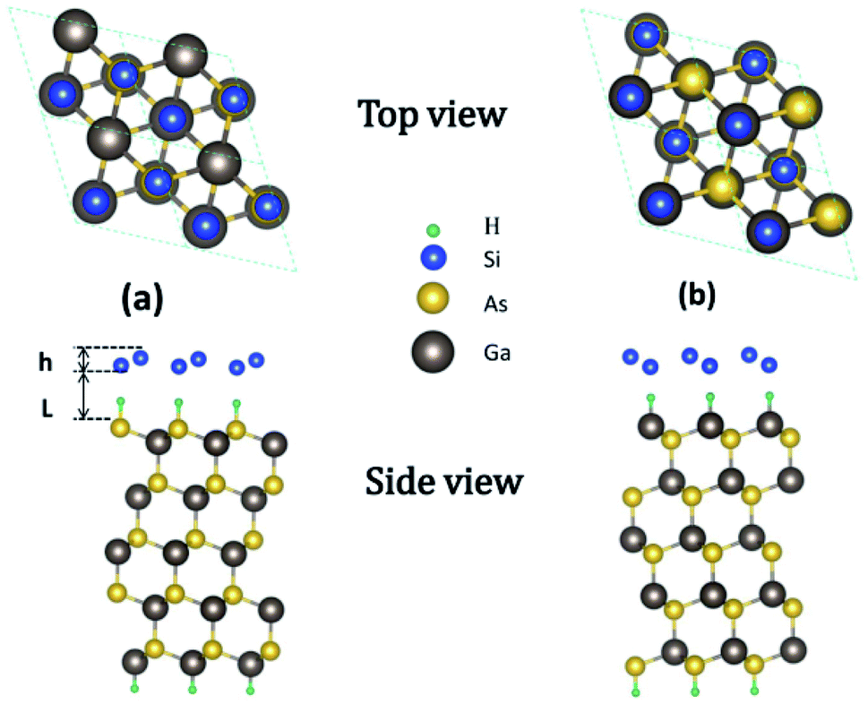 | ||
| Fig. 1 Top and side views of silicene/HAs–GaAs heterostructure (a) and silicene/HGa–GaAs heterostructure (b). | ||
| L (Å) | LH (Å) | h (Å) | a (Å) | Eb (eV/Si) | |
|---|---|---|---|---|---|
| Silicene/HAs–GaAs | 3.76 | 2.15 | 0.469 | 4.01 | 0.192 |
| Silicene/HGa–GaAs | 3.49 | 1.79 | 0.611 | 4.01 | 0.211 |
The stability of the silicene/HGaAs heterostructures is assessed by defining the interface binding energy as:
| Eb = (EHGaAs + Esilicene − Etot)/N, | (1) |
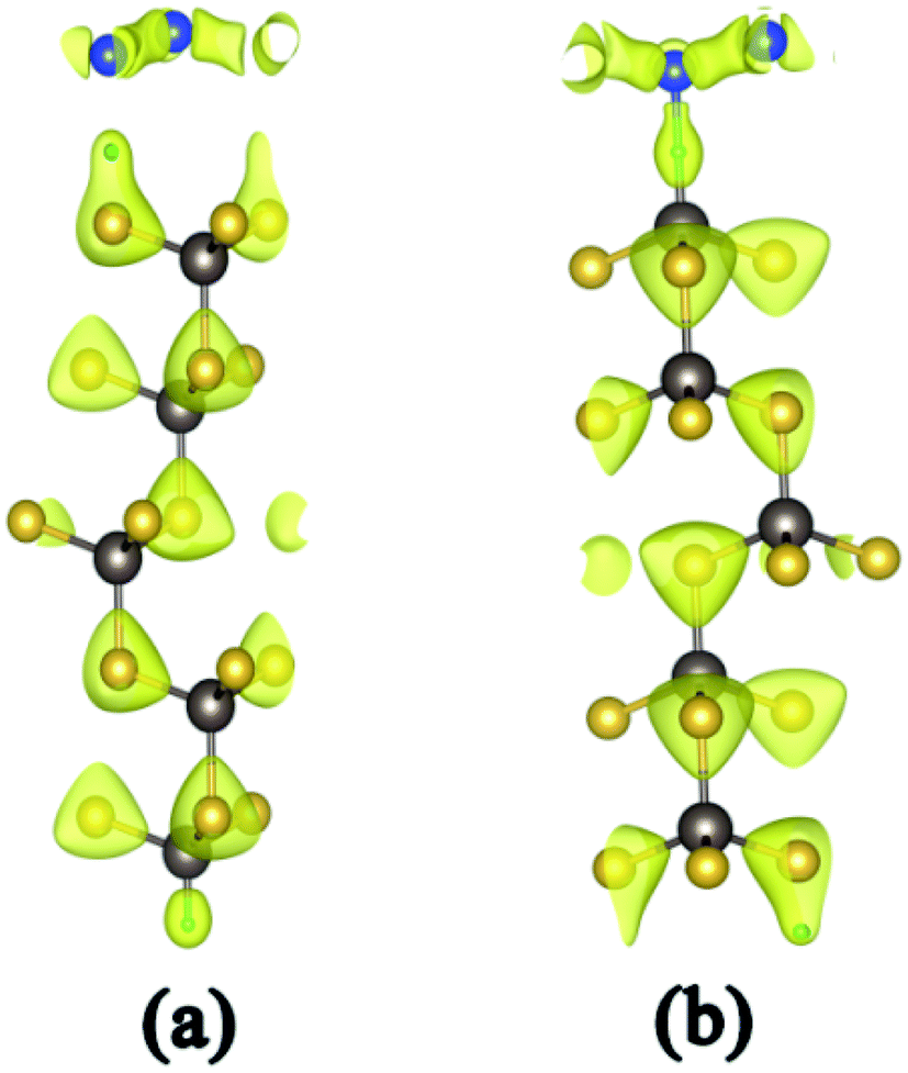 | ||
| Fig. 2 Charge density of silicene/HAs–GaAs heterostructure (a) and silicene/HGa–GaAs heterostructure (b). | ||
The h values of the silicene layer affect the interaction between silicene and the substrate (0.469 Å on As-terminated GaAs(111) surface, 0.611 Å on Ga-terminated GaAs(111) surface). The h of silicene on the As-terminated surface is close to that of the freestanding silicene layer (0.44 Å). In general, the large h indicates a strong interaction between silicene and the substrate, which increases the possibility of losing the Dirac cone and does not conduce to the silicene epitaxial growth in experiments.18
3. Results and discussion
3.1 Electronic properties
The energy band structures of silicene on GaAs(111) surfaces along the Brillouin zone are shown in Fig. 3(a) and (b). The calculation results of the GGA exchange−correlation and the HSE hybrid functional are indicated by blue solid lines and red dashed lines, respectively. In Fig. 3(a), the silicene/HAs–GaAs heterostructure exhibits a direct bandgap at the high symmetry K point in the Brillouin zone. The Eg values for GGA calculation and HSE correction are 0.20 and 0.24 eV, respectively. The existence of the direct bandgap indicates that the interaction between the silicene layer and the As-terminated GaAs(111) surface is largely weakened by the hydrogen intercalation, resulting in no electronic orbital hybridization between Si atoms in the silicene layer and the substrate surface. The weak interaction maintains the Dirac characteristic of silicene and induces a considerable bandgap. For the silicene/HGa–GaAs heterostructure, indirect Eg values with valence band maximum (VBM) at the K point and the conduction band minimum (CBM) at the Γ point are observed (Fig. 3(b)). The Eg values for the GGA calculation and HSE correction are 0.41 and 0.82 eV, respectively. The hydrogen intercalation also induces the Eg of silicene on the Ga-terminated surface, but the dispersion characteristic of the Dirac cone is lost because of the covalent bond between Si and H atoms on the Ga-terminated surface. The downward buckling Si atoms form sp3 hybridization causing silicene to lose the Dirac electronic characteristics of sp2 hybridization. This result also indicates that the hydrogen intercalation has different effects on the electronic properties of silicene on different GaAs(111) terminated surfaces. Moreover, the Fermi energy level of silicene/HAs–GaAs heterostructure shifts upward into the conduction band, showing n-type semiconductor properties, whereas that of silicene/HGa–GaAs heterostructure shifts down into the valence band, showing p-type semiconductor properties. Evidently, this difference is also caused by the different electronegativities of Ga and As atoms.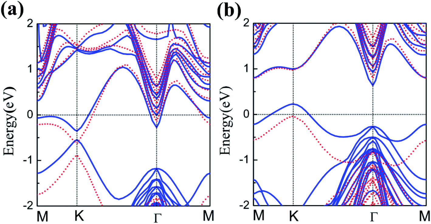 | ||
| Fig. 3 The band structures of silicene/HAs–GaAs heterostructure (a) and silicene/HGa–GaAs heterostructure (b). Blue solid lines are the results of GGA calculations, and red dashed lines are the results of HSE06 calculations. | ||
The results of the HSE hybrid functional are compared with those of GGA calculations. HSE results correct the Eg by 0.04 and 0.41 eV for silicene/HAs–GaAs and silicene/HGa–GaAs heterostructures, respectively. Thus, GGA calculations are basically correct for the energy bands of silicene/HGaAs systems, especially for the silicene/HAs–GaAs heterostructure. The GGA calculations always underestimate the value of Eg but do not affect the qualitative analysis of the results. The calculations of GGA with PBE formula are adopted in the following discussion on the influence of the buckling height h, the interlayer spacing L between silicene and the substrate, biaxial strain ε, and external electric field F on electronic characteristics.
 | ||
| Fig. 4 The band structures near Fermi level of silicene/HAs–GaAs heterostructure (a) and silicene/HGa–GaAs heterostructure (c), the bandgap Eg of silicene/HAs–GaAs heterostructure (b) and silicene/HGa–GaAs heterostructure (d) with different buckling height h of silicene. | ||
The band structures and Eg of the silicene/HGaAs heterostructures as a function of L between silicene and the substrate are shown in Fig. 5. The variation in the valence and conduction band edges of the silicene/HAs–GaAs heterostructure with L is shown in Fig. 5(a). The silicene h is considered as the optimal relaxation value of 0.47 Å. The valence and conduction band edges move downward with increasing L at K and Γ points, respectively. A large L results in the evident upward shift of Fermi level. Eg presents an interesting variation with increasing L as shown in Fig. 5(b). Eg first decreases and then increases and reaches a maximum of 0.21 eV when L is 3.9 Å. When L is over 3.9 Å, Eg begins to decrease again and transits from direct Eg to indirect Eg. The variation in the valence and conduction band edges of the silicene/HGa–GaAs heterostructure with L between silicene and the substrate are shown in Fig. 5(c), where the silicene h is considered as the optimal relaxation value of 0.61 Å. The VBM is located at K point and gradually moves up with increasing L. The CBM is located at Γ point, moves downward first, and then moves upward with increasing L. When L increases to 3.7 Å, the CBM moves to the K point. The variation in Eg is similar to that of the silicene/HAs–GaAs heterostructure. With increasing L, Eg decreases first and increases. The maximum Eg is 0.65 eV at L of 3.7 Å, and Eg is changed from indirect Eg into direct Eg.
 | ||
| Fig. 5 The band structures near Fermi level of silicene/HAs–GaAs heterostructure (a) and silicene/HGa–GaAs heterostructure (c), the bandgap Eg of silicene/HAs–GaAs heterostructure (b) and silicene/HGa–GaAs heterostructure (d) with different interlayer spacing L between silicene and GaAs(111) substrates. | ||
| ε = (a1 − a)/a, | (2) |
 | ||
| Fig. 6 The band structures near Fermi level of silicene/HAs–GaAs heterostructure (a) and silicene/HGa–GaAs heterostructure (c), the bandgap Eg of silicene/HAs–GaAs heterostructure (b) and silicene/HGa–GaAs heterostructure (d) under different biaxial strain ε. | ||
The inherent spin–orbit coupling in freestanding silicene induces a low Eg of 1.55 meV,41 and a little strain decreases Eg.42 By contrast, the silicene on GaAs(111) surfaces can open large Eg values (0.25 eV for silicene/HAs–GaAs and 0.58 eV for silicene/HGa–GaAs) under ε. However, the two heterostructures can only withstand a little ε, and a large ε leads to loss of Eg and transformation into metals.
 | ||
| Fig. 7 The band structures near Fermi level of silicene/HAs–GaAs heterostructure (a) and silicene/HGa–GaAs heterostructure (c), the bandgap Eg of silicene/HAs–GaAs heterostructure (b) and silicene/HGa–GaAs heterostructure (d) under different external electric fields F. | ||
For the freestanding silicene, an electric field F of 0.5 V Å−1 can only induce low Eg of about 20 meV,43,44 which limits the practical application of silicene. By contrast, the Eg values of silicene on GaAs(111) surfaces are 0.2 and 0.41 eV. The applications with external F cannot induce a large Eg but can realize the adjustment of Eg. In addition, silicene/HGaAs heterostructures are sensitive to the negative F, easily lose Eg, and show metallic properties.
3.2 Optical properties
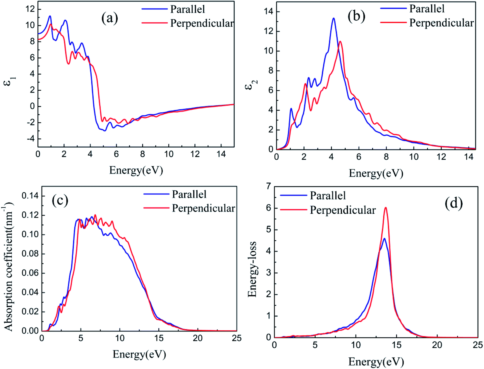
The optical properties of silicene on semiconductors should be studied to design various optoelectronic devices on the basis of silicene applications. Having discussed the results on geometric and electronic structures of silicene on GaAs(111) surfaces, we now focus on discussing the results obtained for the optical response properties of silicene. Optical response characteristics are calculated using 33 × 33 × 1 M–P k-point meshes.Figs. 8(a) and 9(a) depict the real parts of the dielectric function of silicene/HAs–GaAs and silicene/HGa–GaAs heterostructures, respectively, as a function of the incident photon energy. The parallel components (εxx and εyy) are represented by ε∥, and the perpendicular component (εzz) is represented by ε⊥. The static values of the real part of the dielectric function are ε∥(0) = 8.92 and ε⊥(0) = 8.51 for silicene/HAs–GaAs and ε∥(0) = 8.99 and ε⊥(0) = 8.29 for silicene/HGa–GaAs. Multiple dielectric peaks are observed within 0–7 eV photon energy range. When the photon energy is over about 4 eV, the real part of the dielectric function decreases sharply due to the enhanced light absorption of the interband transition. Figs. 8(b) and 9(b) depict the imaginary parts of the dielectric function of silicene/HAs–GaAs and silicene/HGa–GaAs heterostructures, respectively, as a function of the incident photon energy. The imaginary part of the dielectric function has multiple peaks related to the interband transition in the photon energy of 0–6 eV. For the silicene/Has–GaAs heterostructure, the strongest dielectric peak appears at 4.2 and 4.7 eV for parallel and perpendicular polarizations, respectively. For the silicene/HGa–GaAs heterostructure, the strongest dielectric peak appears at 4.1 and 4.6 eV for parallel and perpendicular polarizations, respectively. Comparing the two heterostructures, the number of peaks in the imaginary part of the silicene/HAs–GaAs heterostructure is significantly more than that of the silicene/HGa–GaAs heterostructure, indicating that the silicene/HAs–GaAs heterostructure has more interband transition processes than the silicene/HGa–GaAs heterostructure.
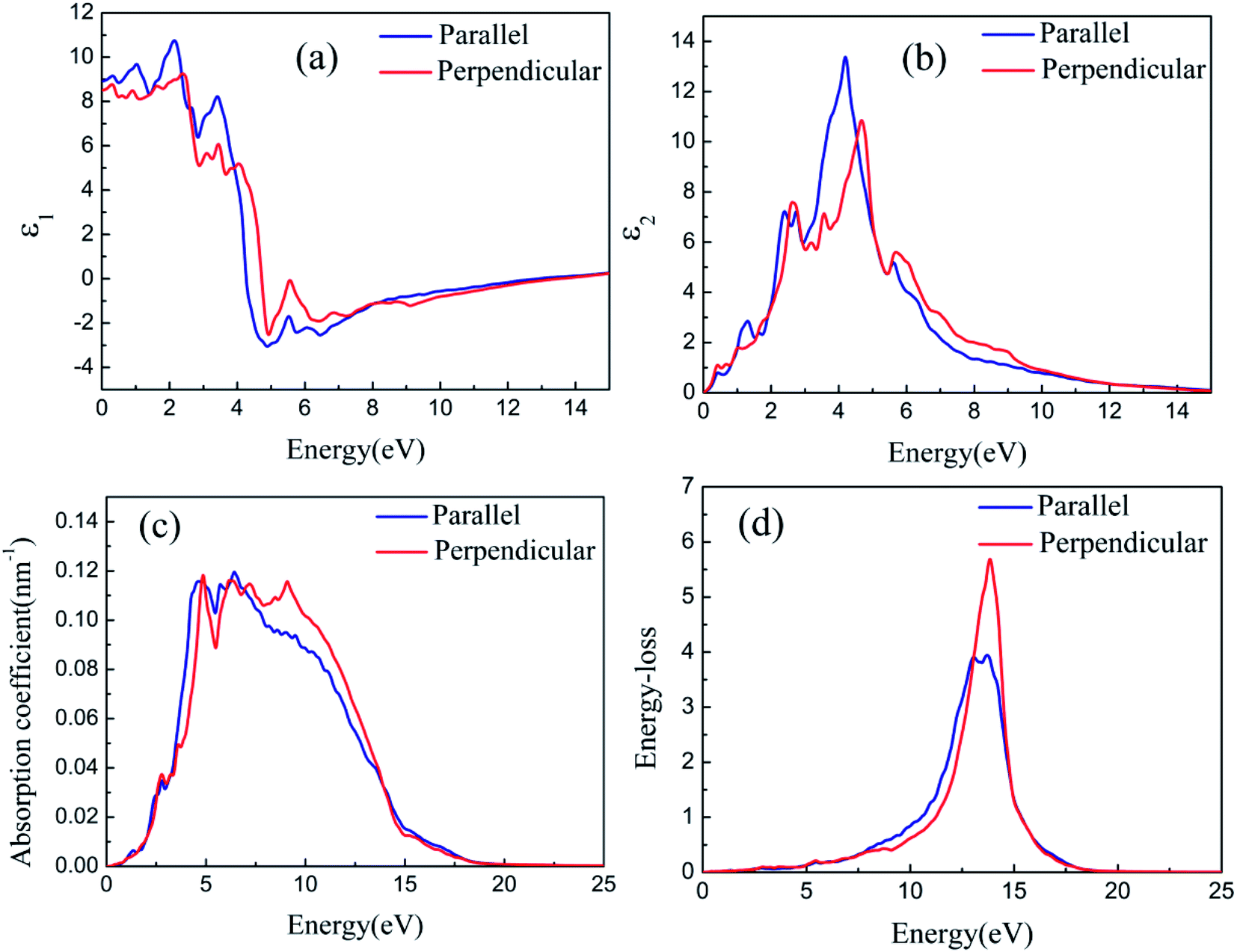 | ||
| Fig. 8 The real part (a) and imaginary part (b) of the dielectric function, the optical absorption spectra (c), and the energy loss spectra (d) with the photon energy for silicene/HAs–GaAs heterostructure. | ||
 | ||
| Fig. 9 The real part (a) and imaginary part (b) of the dielectric function, the optical absorption spectra (c), and the energy loss spectra (d) with the photon energy for silicene/HGa–GaAs heterostructure. | ||
The light response range of the heterostructure is relatively large and has multiple absorption peaks in 1–12 eV. Strong absorption peaks are distributed in the ultraviolet light region (>3.9 eV). For the silicene/Has–GaAs heterostructure, the typical absorption peaks of freestanding silicene are preserved in the absorption spectrum because the interaction between silicene and substrate is the van der Waals force. Chen et al. have given the absorption spectrum of the freestanding silicene layer through the first-principles calculations.47,48 Two typical absorption peaks are observed in the freestanding silicene layer. The first peak is a weak absorption peak caused by π–π* transition at 1.9 eV, and the second peak is the strongest absorption peak caused by σ–σ* transition at 4.4 eV. In our work, typical absorption peaks corresponding to freestanding silicene appear at 2.5 and 5 eV, respectively, which have remarkably blue-shifted compared with those of the freestanding silicene layer. It is because that the interaction between silicene and GaAs(111) substrate makes the CBM upward. The silicene/HGa–GaAs heterostructure only preserves one typical absorption peak of the freestanding silicene, and this peak is narrow and blue shifts. The maximum peak appears at about 7 eV, which corresponds to the maximum absorption peak of bulk GaAs.49 The above analysis shows that silicene/HGaAs heterostructures have typical optical properties of silicene and exhibit some unique optical properties (such as unique dielectric function and absorption spectrum) in the visible light irradiation range, indicating potential applications in optical transmission and optoelectronic devices.
4. Conclusion
In summary, we have investigated the structural, electronic, and optical properties of silicene/HGaAs heterostructures by using the first-principles method. Results show that the hydrogen intercalation successfully weakens the interaction between the silicene layer and the GaAs(111) surface and causes to open a considerable Eg. The silicene/HGa–GaAs heterostructure has indirect Eg, while the silicene/HAs–GaAs heterostructure has direct Eg. Compared on Ga-terminated GaAs(111) surface, the silicene layer on As-terminated GaAs(111) surface has lower buckling height which is conducive to experimental growth. The electronic properties of silicene/HGaAs heterostructures can be controlled by adjusting the layer spacing L and the buckling height h, and applying biaxial strain ε and external electric field F. Adjusting L, h and applying ε can induce a large Eg and realize the transition between direct and indirect bandgap Eg. However, the two heterostructures can only withstand a small ε, and a large ε causes the loss in Eg and transformation into metallic properties. Applying an external F can adjust Eg but cannot induce a large Eg. In addition, silicene/HGaAs heterostructures are sensitive and easily lose Eg to become metallic under the negative perpendicular F. The optical properties of the two heterostructures are analyzed, and results show multiple absorption peaks in the energy range of 1–12 eV, and the typical optical properties of freestanding silicene are retained in the spectra of silicene/HGaAs heterostructures. The anisotropy of parallel and perpendicular directions in the two heterostructures exists, and the absorption and energy loss peaks are concentrated in the ultraviolet region. Our prediction results may provide guidance on the expected results of silicene/semiconductor heterostructures under experimental conditions. Theoretical observations are expected to promote the application of silicene in optoelectronic devices.Conflicts of interest
There are no conflicts to declare.Acknowledgements
This work was supported by the National Natural Science Foundation of China (Grant No. 60976070).References
- B. K. Teo and X. H. Sun, Chem. Rev., 2007, 107, 1454 CrossRef CAS.
- Q. Tang and Z. Zhou, Prog. Mater. Sci., 2013, 58, 1244 CrossRef CAS.
- C. N. R. Rao, K. Gopalakrishnan and U. Maitra, ACS Appl. Mater. Interfaces, 2015, 7, 7809 CrossRef CAS PubMed.
- D. Akinwande, N. Petrone and J. Hone, Nat. Commun., 2014, 5, 5678 CrossRef CAS PubMed.
- C. Liu, W. Feng and Y. Yao, Phys. Rev. Lett., 2011, 107, 76802 CrossRef PubMed.
- M. Farokhnezhad, M. Esmaeilzadeh, S. Ahmadi and N. Pournaghavi, J. Appl. Phys., 2015, 117, 173913 CrossRef.
- Q. Pei, Y. Zhang, Z. Sha and V. B. Shenoy, J. Appl. Phys., 2013, 114, 33526 CrossRef.
- K. Takeda and K. Shiraishi, Phys. Rev. B: Condens. Matter Mater. Phys., 1994, 50, 14916 CrossRef CAS PubMed.
- B. Feng, Z. Ding, S. Meng, Y. Yao, X. He, P. Cheng, L. Chen and K. Wu, Nano Lett., 2012, 12, 3507 CrossRef CAS PubMed.
- C. Lin, R. Arafune, K. Kawahara, N. Tsukahara, E. Minamitani, Y. Kim, N. Takagi and M. Kawai, Appl. Phys. Express, 2012, 5, 45802 CrossRef.
- L. Chen, C. C. Liu, B. Feng, X. He and K. Wu, Phys. Rev. Lett., 2012, 109, 056804 CrossRef PubMed.
- L. Chen, H. Li, B. Feng, Z. Ding, J. Qiu, P. Cheng, K. Wu and S. Meng, Phys. Rev. Lett., 2013, 110, 85504 CrossRef PubMed.
- J. Qiu, H. Fu, Y. Xu, A. I. Oreshkin, T. Shao, L. Hui, S. Meng, L. Chen and K. Wu, Phys. Rev. Lett., 2015, 114, 126101 CrossRef PubMed.
- S. Sheng, J. B. Wu, X. Cong, W. Li, J. Gou, Q. Zhong, P. Cheng, P. H. Tan, L. Chen and K. Wu, Phys. Rev. Lett., 2017, 119, 196803 CrossRef PubMed.
- A. Molle, C. Grazianetti, D. Chiappe, E. Cinquanta, E. Cianci, G. Tallarida and M. Fanciulli, Adv. Funct. Mater., 2013, 23, 4340 CrossRef CAS.
- E. Cinquanta, E. Scalise, D. Chiappe, C. Grazianetti, B. van den Broek, M. Houssa, M. Fanciulli and A. Molle, J. Phys. Chem. C, 2013, 117, 16719 CrossRef CAS.
- L. Tao, E. Cinquanta, D. Chiappe, C. Grazianetti, M. Fanciulli, M. Dubey, A. Molle and D. Akinwande, Nat. Nanotechnol., 2015, 10, 227 CrossRef CAS PubMed.
- H. Zhong, R. Quhe, Y. Wang, J. Shi and J. Lü, Chin. Phys. B, 2015, 24, 87308 CrossRef.
- S. Y. Zhou, G. H. Gweon, A. V. Fedorov, P. N. First, W. A. de Heer, D. H. Lee, F. Guinea, N. A. Castro and A. Lanzara, Nat. Mater., 2007, 6, 770 CrossRef CAS PubMed.
- H. J. Song, M. Son, C. Park, H. Lim, M. P. Levendorf, A. W. Tsen, J. Park and H. C. Choi, Nanoscale, 2012, 4, 3050 RSC.
- D. Chiappe, E. Scalise, E. Cinquanta, C. Grazianetti, B. van den Broek, M. Fanciulli, M. Houssa and A. Molle, Adv. Mater., 2014, 26, 2096 CrossRef CAS PubMed.
- G. Kresse and J. Furthmüller, Phys. Rev. B: Condens. Matter Mater. Phys., 1996, 54, 11169 CrossRef CAS PubMed.
- X. Blanc, É. Cancès and M. Dupuy, C. R. Acad. Sci. Paris, Ser. I, 2017, 355, 665 CrossRef.
- J. P. Perdew, K. Burke and M. Ernzerhof, Phys. Rev. Lett., 1997, 78, 1396 CrossRef CAS.
- J. Klimeš, D. R. Bowler and A. Michaelides, Phys. Rev. B: Condens. Matter Mater. Phys., 2011, 83, 195131 CrossRef.
- P. Deak, B. Aradi, T. Frauenheim, E. Janzen and A. Gali, Phys. Rev. B: Condens. Matter Mater. Phys., 2010, 81, 2149 CrossRef.
- G. Luo, Z. Han, C. Chien, C. Ko, C. H. Wann, H. Lin, Y. Shen, C. Chung, S. Huang, C. Cheng and C. Chang, J. Electrochem. Soc., 2010, 157, H27 CrossRef CAS.
- T. Yu and Y. Lu, Phys. Chem. Chem. Phys., 2020, 22, 26402 RSC.
- C. Riedl, C. Coletti, T. Iwasaki, A. A. Zakharov and U. Starke, Phys. Rev. Lett., 2009, 103, 246804 CrossRef CAS PubMed.
- Z. Guo and A. Oshiyama, Phys. Rev. B: Condens. Matter Mater. Phys., 2014, 89, 155418 CrossRef.
- Z. Guo, S. Furuya, J. Iwata and A. Oshiyama, Phys. Rev. B: Condens. Matter Mater. Phys., 2013, 87, 235435 CrossRef.
- V. S. Prudkovskiy, F. Iacovella, K. P. Katin, M. M. Maslov and N. Cherkashin, Nanotechnology, 2018, 29, 365304 CrossRef CAS PubMed.
- X. Zhang, Z. Guo, J. Cao, X. Xiao and J. Ding, Acta Phys. Sin., 2015, 64, 186101 Search PubMed.
- D. A. Woolf, D. I. Westwood and R. H. Williams, Appl. Phys. Lett., 1993, 62, 1370 CrossRef CAS.
- H. Nakatsuji, Y. Kamakura and K. Taniguchi, J. Comput. Electron., 2003, 2, 109 CrossRef CAS.
- S. E. Thompson, M. Armstrong, C. Auth and S. Cea, IEEE Electron Device Lett., 2004, 25, 191 CrossRef CAS.
- V. M. Pereira and N. A. Castro, Phys. Rev. Lett., 2009, 103, 46801 CrossRef PubMed.
- N. Levy, S. A. Burke, K. L. Meaker, M. Panlasigui, A. Zettl, F. Guinea, A. H. Castro Neto and M. F. Crommie, Science, 2010, 329, 544 CrossRef CAS PubMed.
- S. Barraza-Lopez, A. A. Pacheco Sanjuan, Z. Wang and M. Vanević, Solid State Commun., 2013, 166, 70 CrossRef CAS.
- X. Li, H. Cao, Y. Guo, X. Zhou and J. Yu, Mater. Chem. Phys., 2020, 242, 122554 CrossRef CAS.
- C. Liu, W. Feng and Y. Yao, Phys. Rev. Lett., 2011, 107, 76802 CrossRef PubMed.
- T. P. Kaloni, Y. C. Cheng and U. Schwingenschlögl, J. Appl. Phys., 2013, 113, 104305 CrossRef.
- R. Quhe, R. Fei, Q. Liu, J. Zheng, H. Li, C. Xu, Z. Ni, Y. Wang, D. Yu, Z. Gao and J. Lu, Nano Lett., 2012, 2, 113 Search PubMed.
- N. D. Drummond, V. Zólyomi and V. I. Fal'Ko, Phys. Rev. B: Condens. Matter Mater. Phys., 2012, 85, 75423 CrossRef.
- H. Cao, Z. Zhou, X. Zhou and J. Cao, Comput. Mater. Sci., 2017, 139, 179 CrossRef CAS.
- M. Fadaie, N. Shahtahmassebi and M. R. Roknabad, Opt. Quantum Electron., 2016, 48, 440 CrossRef.
- X. Chen, J. Jiang, Q. Liang, R. Meng, C. Tan, Q. Yang and X. Sun, J. Mater. Chem. C, 2016, 4, 7004 RSC.
- R. Das, S. Chowdhury, A. Majumdar and D. Jana, RSC Adv., 2014, 5, 41 RSC.
- Y. Yan, Y. Wang and H. Ma, Chin. J. Physiol., 2016, 33, 221 Search PubMed.
| This journal is © The Royal Society of Chemistry 2021 |