
 Open Access Article
 This Open Access Article is licensed under a Creative Commons Attribution-Non Commercial 3.0 Unported Licence
Rapid, facile synthesis of InSb twinning superlattice nanowires with a high-frequency photoconductivity response†
Yinyin Qian‡
 *a,
Kaijia Xu‡a,
Lanjun Chengb,
Cunxin Lia and
Xingchen Wanga
*a,
Kaijia Xu‡a,
Lanjun Chengb,
Cunxin Lia and
Xingchen Wanga
aAnhui Laboratory of Clean Energy Materials and Chemistry for Sustainable Conversion of Natural Resources, College of Chemical and Environmental Engineering, Anhui Polytechnic University, Wuhu 241000, P. R. China. E-mail: qianyinyin@ahpu.edu.cn
bUniversity of Science and Technology of China, Hefei 230026, P. R. China
First published on 28th May 2021
Abstract
We present a self-seeded (with indium droplets) solution–liquid–solid (SLS) synthesis route for InSb nanowires (NWs) using commercially available precursors at a relatively low temperature of about 175 °C, which takes only 1 min upon the injection of reductant. Structural characterization reveals that the InSb nanowires are high quality and have twinning superlattice structures with periodically spaced twin planes along the growth direction of 〈111〉. Notably, we have measured an ultrafast conductivity lifetime in the NWs of just 9.1 ps utilizing time-resolved optical pump-terahertz probe (OPTP) spectroscopy, which may facilitate the development of high-frequency nanoscale integrated optoelectronic systems related to twinning superlattice structures.
Introduction
One-dimensional semiconductor nanowires are well suited for numerous classes of high-performance electronic and optoelectronic devices,1–10 typically including solar cells,11 biochemical sensors,12 high-speed field-effect transistors,13 and terahertz detectors,14 owing to high electrical conductivity and large absorption cross sections associated with their high dimensional anisotropy. In particular, semiconductor nanowires made from III–V materials have been shown to exhibit tunable band gap, high carriers mobilities, and large dielectric constants, which leads to an increased attention in recent years.15 In general, the preparation of III–V semiconductor nanowires fabricated via catalyzed growth mechanism has the tendency to form the randomly occurred rotational stacking faults along the nanowires growth direction.16–21 The stacking faults are commonly composed of random mixtures of hexagonal wurtzite (WZ) and cubic zinc-blende (ZB) crystal phase. The electron wavefunction was interrupted at the stacking faults, which can significantly degrade the electronic and optoelectronic properties of the nanowires devices.18,22 In recent years, the crystal-phase control of zinc-blende (ZB) and wurtzite (WZ) crystal phase with a long-range periodic sequence, namely twinning superlattices (TSLs), has been intensively discussed in various III–V nanowires such as InP,20,23 InAs,24 GaP21 and GaAs25,26 can successfully promote the formation of unique electronic mini-bands and the modification of the density of states,27 which may be potentially useful for bandgap and phonon engineering in future high-performance NWs-based devices.28Among the known binary III–V compound semiconductors, indium antimonide (InSb) has a narrow direct band gap energy (0.17 eV), low thermal conductivities (0.18 W cm−1 K−1), small exciton binding energy (0.5 meV), and extremely high electron mobilities (78![[thin space (1/6-em)]](https://www.rsc.org/images/entities/char_2009.gif) 000 cm2 V−1 s−1) at room temperature,29,30 consequently making it the suitable material for infrared photodetectors, topological superconductivity and a promising platform for quantum computing.31–33 To date, InSb nanowires have been generally synthesized by epitaxial growth methods (>400 °C) including metal–organic vapor phase epitaxy (MOVPE),34,35 chemical beam epitaxy (CBE) and molecular beam epitaxy (MBE) via the vapor–liquid–solid (VLS) mechanism.36–39 However, the growth of InSb twinning superlattice nanowires by the above-mentioned methods has proven to be very challenging primarily attributed to the small ionicity with low bonding tendency and the high energy barrier (8.2 meV per atom) for the ZB/WZ phase transition compared with other III–V compound semiconductor nanowires.37,40–42 Furthermore, the rather small growth temperature window during the VLS growth process limited by the low melting point of InSb at approximately 520 °C and the high decomposition temperature for usual Sb precursors,43 severely hinder the thermodynamic regulation of zinc-blende (ZB) and wurtzite (WZ) phase formed alternately in a periodic nucleation process to obtain the twinning superlattices structure.44 In striking comparison to the energy-intensive and time-consuming vapor-phase growth approaches, solution-based route via solution–liquid–solid (SLS) mechanism can proceed at relatively low temperatures (<300 °C) and provide semiconductor nanowires with easy growth processes and adaptability for large-scale fabrication of nanowire-based devices.45–47 Therefore, extensive efforts have been mostly focused on growing InSb twinning superlattice nanowires via solution-phase growth approaches. Luckily, recent progress indicates that InSb nanostructures such as quantum dots and nanorods can be successfully prepared by solution-phase techniques. Raffaelle and co-workers first achieved InSb quantum dots by utilizing tris(trimethylsilyl)antimony as a Sb precursor by a solution-phase synthetic approach.43,48 Subsequent work by Talapin's group prepared monodisperse and well crystallized colloidal InSb quantum dots with diameters sub-10 nm by a hot-injection strategy.49 Specifically, the first achievement of pseudo-one-dimensional InSb nanorods in solution was reported by Kovalenko and his co-workers in 2013.40 The synthetic scheme was conducted by reaction of In([N(SiMe3)2]3) and Sb(NMe2)3 in the presence of In nanoparticles in tri-n-octylphosphine. However, the pre-synthesized procedure for In or Sb precursors adopted in the previous efforts will make the synthesis process more complicated and probably affects the reproducibility. In order to achieve InSb twinning superlattice nanowires in solution utilizing only commercially available precursors, Yang and his co-workers injected a mixture of oleylamine, borane–tert-butylamine complex, and tri-n-octylphosphine into a solution of In(acac)3 and Sb(Ph)3 in 1-octadecene.50 Unfortunately, the optimized technique required relatively longer growth time and higher synthesis temperature to form the target nanostructures, which easily causing the resulting nanowires with significant size boarding and rendering the large-scale production difficult.51 Therefore, it is essential to develop a rapid and cost-effective solution-based route for synthesizing InSb twinning superlattice nanowires at relatively low temperatures.
000 cm2 V−1 s−1) at room temperature,29,30 consequently making it the suitable material for infrared photodetectors, topological superconductivity and a promising platform for quantum computing.31–33 To date, InSb nanowires have been generally synthesized by epitaxial growth methods (>400 °C) including metal–organic vapor phase epitaxy (MOVPE),34,35 chemical beam epitaxy (CBE) and molecular beam epitaxy (MBE) via the vapor–liquid–solid (VLS) mechanism.36–39 However, the growth of InSb twinning superlattice nanowires by the above-mentioned methods has proven to be very challenging primarily attributed to the small ionicity with low bonding tendency and the high energy barrier (8.2 meV per atom) for the ZB/WZ phase transition compared with other III–V compound semiconductor nanowires.37,40–42 Furthermore, the rather small growth temperature window during the VLS growth process limited by the low melting point of InSb at approximately 520 °C and the high decomposition temperature for usual Sb precursors,43 severely hinder the thermodynamic regulation of zinc-blende (ZB) and wurtzite (WZ) phase formed alternately in a periodic nucleation process to obtain the twinning superlattices structure.44 In striking comparison to the energy-intensive and time-consuming vapor-phase growth approaches, solution-based route via solution–liquid–solid (SLS) mechanism can proceed at relatively low temperatures (<300 °C) and provide semiconductor nanowires with easy growth processes and adaptability for large-scale fabrication of nanowire-based devices.45–47 Therefore, extensive efforts have been mostly focused on growing InSb twinning superlattice nanowires via solution-phase growth approaches. Luckily, recent progress indicates that InSb nanostructures such as quantum dots and nanorods can be successfully prepared by solution-phase techniques. Raffaelle and co-workers first achieved InSb quantum dots by utilizing tris(trimethylsilyl)antimony as a Sb precursor by a solution-phase synthetic approach.43,48 Subsequent work by Talapin's group prepared monodisperse and well crystallized colloidal InSb quantum dots with diameters sub-10 nm by a hot-injection strategy.49 Specifically, the first achievement of pseudo-one-dimensional InSb nanorods in solution was reported by Kovalenko and his co-workers in 2013.40 The synthetic scheme was conducted by reaction of In([N(SiMe3)2]3) and Sb(NMe2)3 in the presence of In nanoparticles in tri-n-octylphosphine. However, the pre-synthesized procedure for In or Sb precursors adopted in the previous efforts will make the synthesis process more complicated and probably affects the reproducibility. In order to achieve InSb twinning superlattice nanowires in solution utilizing only commercially available precursors, Yang and his co-workers injected a mixture of oleylamine, borane–tert-butylamine complex, and tri-n-octylphosphine into a solution of In(acac)3 and Sb(Ph)3 in 1-octadecene.50 Unfortunately, the optimized technique required relatively longer growth time and higher synthesis temperature to form the target nanostructures, which easily causing the resulting nanowires with significant size boarding and rendering the large-scale production difficult.51 Therefore, it is essential to develop a rapid and cost-effective solution-based route for synthesizing InSb twinning superlattice nanowires at relatively low temperatures.
On the basis of previous works on fabricating InSb nanostructures in solution,40,47,49,50 we present a facile, one-pot, self-catalyzed synthetic strategy by the well-established SLS mechanism45,46,52,53 to grow InSb twinning superlattice NWs featuring fastest growth time (1 min) and lowest synthesis temperature (175 °C), which even compared to other binary or pseudobinary III–V semiconductor nanowires with twinning superlattice structures formed via SLS as well as VLS growth mechanism.16,19,20,23–25,50,54 Furthermore, by means of the noncontact technique-optical pump-terahertz probe (OPTP) spectroscopy, we extract the ultrashort relaxation and recombination dynamics of photoconductivity lifetime in as-prepared InSb twinning superlattice NWs of just 9.1 ps at room temperature, indicating their great potential for high-speed photodetectors, transistors, and emitters.55
Results and discussion
Fig. 1a shows the typical powder X-ray diffraction (XRD) pattern of the samples obtained in 1 min at 175 °C. The peaks at 23.752°, 27.624°, 39.372°, 46.398°, 56.862°, 62.449°, 71.188° and 76.356° (2θ) are in good agreement with (111), (200), (220), (311), (400), (331), (422), and (511) crystal planes of the cubic zincblende phase InSb, respectively (JCPDS card, no. 89-4299); the additional weak diffraction peak at 32.778° (2θ, marked with *) was observed due to a small amount of metallic In(0) existed in the sample. Typically, the diffraction peak of (220) is more intense than it would be in the standard pattern, which demonstrates that the InSb NWs grow preferentially alone c-direction in our solution-based synthetic route.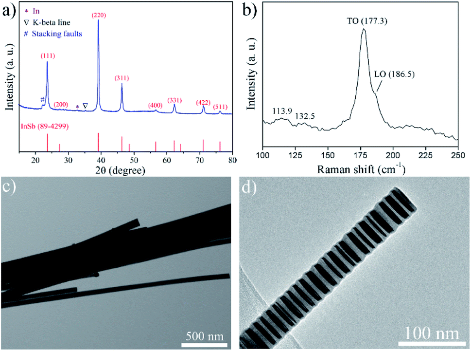 | ||
| Fig. 1 (a) XRD pattern of as-grown InSb twinning superlattice nanowires (b) the room-temperature Raman spectra for the InSb nanowires with reaction time of 1 min, (c) TEM image, and (d) cross-section TEM image for the representative InSb nanowire. | ||
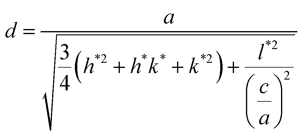
Moreover, there is a diffraction peak located at 2θ = 22.424° (d = 3.961 Å, marked with #) other than the diffraction peaks of the original pure InSb in cubic zinc-blende (3C) phase, which can be indexed as stacking faults. This diffraction peak can be considered as the reflection of a (100) plane in a hexagonal phase (taking 2H for example). In InSb nanowires, the stacking sequence in the [111] direction is …ABCABC… for the cubic zincblende crystal structure whereas …ABAB… for the hexagonal wurtzite crystal structure (where each of the letters A, B, and C represents a bilayer of atoms, composing of one layer with In and one with Sb atoms). Often the zincblende stacking sequence is found to change from an …ABCABC… to an …ABC![[A with combining low line]](https://www.rsc.org/images/entities/char_0041_0332.gif) CBA…, the stacking sequence is still zincblende type after “”, the segments above and below the twin plane “” have different twin orientations. However, the small part of the sequence surrounding the twin plane “” (stacking faults) followed a wurtzite type could be regarded as nH polytypes (where n is the number of bilayers in the smallest repeating stacking unit). It is commonly assumed that the lattice constant of the hexagonal polytypes aH is related to the cubic lattice constant aC via aH = aC/21/2. InSb of zincblende crystal structure has the lattice constant of aC = 6.4782 Å, and its corresponding lattice constant of the hexagonal polytypes aH is aC/21/2 = 4.5808 Å. Interplanar crystal spacing at stacking faults (nH polytypes) d can be substituted into the following equation:
CBA…, the stacking sequence is still zincblende type after “”, the segments above and below the twin plane “” have different twin orientations. However, the small part of the sequence surrounding the twin plane “” (stacking faults) followed a wurtzite type could be regarded as nH polytypes (where n is the number of bilayers in the smallest repeating stacking unit). It is commonly assumed that the lattice constant of the hexagonal polytypes aH is related to the cubic lattice constant aC via aH = aC/21/2. InSb of zincblende crystal structure has the lattice constant of aC = 6.4782 Å, and its corresponding lattice constant of the hexagonal polytypes aH is aC/21/2 = 4.5808 Å. Interplanar crystal spacing at stacking faults (nH polytypes) d can be substituted into the following equation:
The Raman spectrum collected from SiO2 substrate with the presence of as-prepared InSb NWs is presented in Fig. 1b. The asymmetric peaks at around 177.3 and 186.5 cm−1 are assigned to the transversal optical (TO) and longitudinal optical (LO) modes, respectively, for the zincblende InSb nanowires. Interestingly, the TO and LO modes of the InSb twinning superlattice NWs exhibited a slight downshift compared to the characteristic Raman peaks of bulk InSb, 180 and 190 cm−1,56 which possibly owing to the twinning superlattice structures with relative short segments in the nanowires and a laser-induced heating effect.57 Additionally, the scattering peaks at 113.9 and 132.5 cm−1 are corresponding to In2O3 due to the partial surface oxidation of InSb NWs, which further confirmed by high-resolution X-ray photoelectron spectroscopy (XPS) spectra (Fig. S1†) of In 3d and O 1s binding energies for the InSb NWs. The binding energies of In 3d (3d5/2: 444.1 eV; 3d3/2: 451.9 eV) and O 1s (532.7 eV) can be assigned to In2O3,58 although the oxide impurities cannot be characterized by X-ray diffraction (Fig. 1a). The existence of In2O3 caused by surface oxidation and the nanoscale metallic In(0) could also be confirmed by the absorptions peak located at about 440 nm and 600 nm in the room temperature UV-vis-NIR absorption spectra, respectively (Fig. S2†).59–62 Additionally, we see a single weak shoulder at around 1400 nm that can be attributed to a small amount of wide distribution in diameter and length of InSb NWs.42
Fig. 1c displays a low-magnification transmission electron microscopy (TEM) image of the as-synthesized InSb NWs, which further demonstrated the NWs are crystalline in high quality with twinned structures. The nanowires are straight and exhibit a moderate size distribution of diameter centered at about 40 nm in diameter. The transmission electron microscopy (TEM) image of the InSb twinning superlattice nanowire (Fig. 1d) clearly shows a twinning superlattice structure formed by regularly spaced twin planes along the cubic InSb 〈111〉 crystalline growth direction of these nanowires.
The twinning superlattice structures in a single InSb nanowire are clearly seen in HRTEM analyse (Fig. 2a), where the sequential dark and bright contrast refers to sequential zincblende segments above and below the twin planes. TEM images of InSb twinning superlattice NWs and the corresponding histogram of spacings between twin planes were shown in Fig. S3.† Typically, the spacings between twin planes of InSb twinning superlattice nanowires are centered at 8–9 nm. We have also carefully indicated the zincblende type and wurtzite type (twin plane) in the corresponding atomic model for the periodic growth of the InSb nanowire with twinning superlattices. As depicted in Fig. S4,† the twinning superlattice period of the InSb NWs was defined as twice the distance between two adjacent twin planes, which was further measured by small-angle X-ray scattering (SAXS), demonstrating the pseudoperiodicity of InSb NWs is 177.6 Å (Fig. 2b).
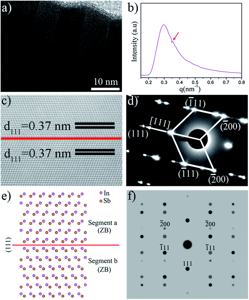 | ||
Fig. 2 (a) High-resolution TEM image of the twin planes in a single InSb NW. (b) Representative SAXS patterns of the InSb twinning superlattice nanowires with the pseudoperiodicity of 177.6 Å (q = 0.3536 nm−1, indicated by red arrow, d = 2π/q = 17.7601 nm). (c) HAADF-STEM image of as-obtained sample acquired along the [0−11] direction, and (d) corresponding SAED patterns, in addition to (e) representative atomic models of InSb twinning superlattice NW, and (f) simulated electron diffraction patterns for the twinning structure using the JEMS software package for the cubic zincblende InSb NWs with the F![[4 with combining macron]](https://www.rsc.org/images/entities/char_0034_0304.gif) 3m space group. 3m space group. | ||
Fig. 2c shows an atom-resolution high-angle annular dark-field (HAADF) STEM image of the as-prepared InSb twinning superlattice NW, taken from the [0−11] direction. The clear lattice fringes exhibit that the NWs are well crystallized. The superimposed atomic arrays on the image indicate the locations of atom columns, due to In atomic number (Z = 49) is as large as Sb atomic (Z = 51), the In columns is as brighter as Sb columns, but they still can be resolved in the HAADF-STEM image. The zincblende InSb nanowire are separated in two segments by twinning plane of (111) corresponding to the red line in the HAADF-STEM image. It is found that the interplanar distance of 0.37 nm in the two separate segments can be indexed to the (111) plane of zincblende InSb. The corresponding SAED patterns (shown in Fig. 2d) for a typical nanowire recorded along the [01−1] zone axis, which consists of two sets of diffraction spots as indexed, indicating the nanowires have twinning superlattice structures and share a common (111) plane along the growth orientation 〈111〉, which further confirmed by the atomic models and simulated electron diffraction patterns as compared to experimental SAED patterns (Fig. 2d), as seen in Fig. 2e and f.
The syntheses were carried out in an argon environment using a previously reported method47 after some modification (described fully in the ESI†). InSb NWs were synthesized at a relatively low temperature (typically at approximately 175 °C) in an ultrafast reaction time (1 min) using commercially available tris(2,4-pentanedionato)-indium(III) (In(acac)3) and triphenylantimony (Sb(Ph)3) as precursors. The present route was based on the in situ reduction of In(III) precursor by the injection of borane tert-butylamine complex (BTB) and proceeds through the generation of melted indium nanoparticles, the melted indium nanoparticles can provide as ideal surfaces to lower the energy barrier for precursor absorption and decomposition, which subsequently catalyze the growth of InSb nanowires via the well-established SLS mechanism (Fig. 3a). When we prolonged the reaction time to 2 min, 5 min, 10 min and 30 min, it is clear from the overview TEM images in Fig. S5† that the great quantity of wirelike nanostructures are general. The formation of zincblende phase InSb NWs in different reaction times was further confirmed by XRD pattern (Fig. S6†) and room-temperature Raman spectra (Fig. S7†). In addition, the employment of TOP would favor the growth of InSb NWs in high quality due to their capping effect,38 since it is observed that there are only non-wire morphology InSb nanocrystals obtained at the absence of TOP (Fig. S8†).
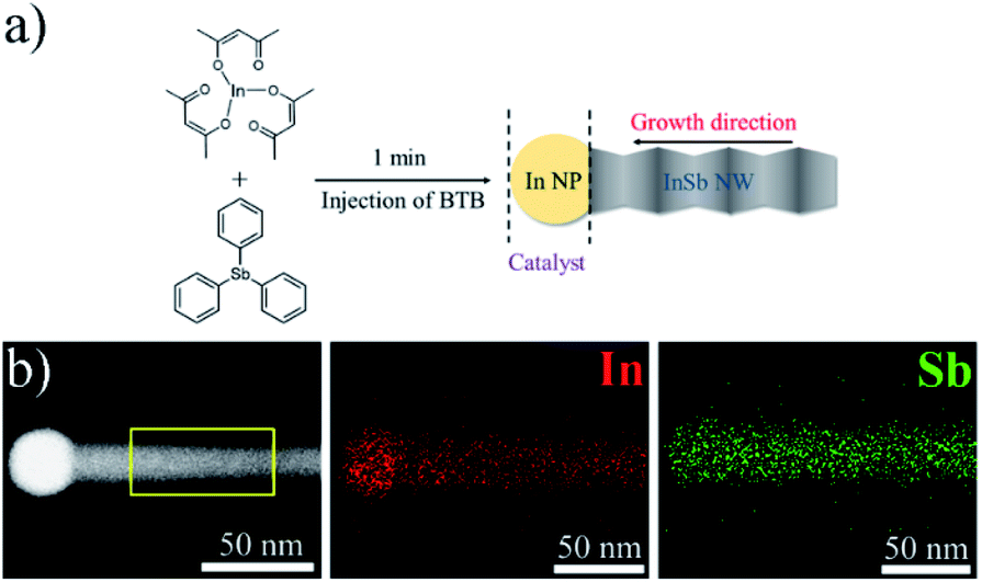 | ||
| Fig. 3 (a) Schematic of the self-catalyzed solution–liquid–solid (SLS) synthetic process to produce InSb NWs, (b) HAADF-STEM and EDX elemental mapping images of a representative InSb NW stem, and the area of STEM-EDX analysis correspond to the yellow box indicated in the HAADF-STEM image. | ||
STEM-EDX analysis confirms that two elements of In and Sb are co-existent in the as-synthesized InSb NW stem, and the molar ratio is determined as 51.27:48.73 (Fig. 3b, and S9†), which is consistent well with the chemical composition In:Sb of 1:1. To clarify whether the droplet is indium and the element distribution of the resulting InSb NW, the STEM-EDX line scan was utilized. The STEM-EDX line scan (Fig. S10†) along the wire axis acquired by scanning a single InSb NW from the In tip reveals that the tip was rich in indium, thus giving evidence that the droplets were indium. The indium nanoparticles attached at nanowire tips further indicates the InSb nanowires grew following a SLS growth mechanism with indium catalyst. The negligible fluctuations of In and Sb contents in the wire stem suggests high compositional homogeneities.
To further explore the electrical properties of the as-prepared InSb twinning superlattice NWs, the dynamics of photoinduced free carriers were measured via the noncontact optical-pump terahertz-probe (OPTP) spectroscopy. The pump beam at repetition rate of 1 kHz pulses was delivered from an amplified Ti: sapphire laser. The THz probe pulses were generated via optical rectification of the femtosecond laser pulses in a 0.5 mm-thick (110) ZnTe crystal. The transmitted terahertz pulses were detected in another 0.5 mm-thick (110) ZnTe crystal by means of electro-optic sampling system. The samples on a quartz substrate were photoexcited by femtosecond pulses at a center wavelength of 800 nm (hν = 1.55 eV) with a pulse of 35 fs duration. After that, by varying the delay between the optical pump and terahertz pulse, a THz spectral response of the material as a function of time after photoexcitation was produced. A conceptual schematic is illustrated in Fig. 4a. Fig. 4b compares the decays of terahertz electric field in InSb NWs to that observed for the non-wire morphology InSb nanocrystals sample. We monitored the photoinduced change in THz temporal transmission signal, ΔE/E = (E − Epump)/E, at the peak of THz time-domain signal by changing the relative delay between the optical pump beam and terahertz probe beam. As for the same excitation fluence of 50 mJ cm−2, the non-wire morphology nanocrystals have almost no response. Even for the fluence was enhanced to 200 mJ cm−2, and the response is also very small. It is unambiguous that the photoactivity of InSb NWs is much larger than non-wire morphology nanocrystals. Furthermore, as for the NWs, the decays of ΔE/E can be calculated by a monoexponential of the form ΔE/E = Aexp(−τ/τrelax) (indicated as black line in Fig. 4b) extracting a carrier lifetime (τrelax) of 9.1 ps. Moreover, the original OPTP data for the pump-induced change in the peak of the terahertz electric field pulse transmitted through the sample (ΔT/T0) as a function of time t after excitation was shown in Fig. S11.† The observed extremely rapid initial decay in photoconductivity of InSb twinning superlattice nanowires differ strongly from those for non-wire morphology InSb nanocrystals that depend critically on the high surface area-to-volume ratios and the enhanced surface charge recombination velocity of as-prepared InSb NWs,63–65 demonstrating the possibility of terahertz detection of ultrafast phenomena occurring in one-dimensional semiconductor nanowires. These results suggest that the InSb NW are prime candidates for application in high-speed nanostructured optoelectronic devices.
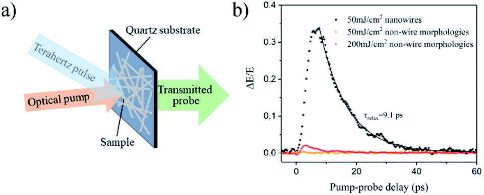 | ||
| Fig. 4 (a) Conceptual illustration of the noncontact optical-pump terahertz-probe (OPTP) setup, (b) pump-induced change in terahertz electric field (ΔE/E) of typical InSb nanowires compared with non-wire morphology InSb nanocrystals at different pump–probe delays. The typical InSb nanowires were excited at wavelength of 800 nm with fluence of 50 mJ cm−2 pulse, and the non-wire morphology InSb nanocrystals were excited at wavelength of 800 nm with fluences of 50 mJ cm−2 and 200 mJ cm−2 pulses. | ||
Conclusions
To conclude, we have reported that high quality InSb twinning superlattice NWs can be synthesized by a rapid, low-temperature solution-based growth strategy, employing commercially available In(acac)3 and Sb(Ph)3 as the precursors. This strategy is relatively facile since the solvents and surfactants used are common and no additional catalyst seeds are required. The reaction pathway can be described in two steps, melted indium nanoparticles were generated in situ by reduction of the indium precursor and subsequently catalyzed the NWs growth. It is especially noted that the as-prepared InSb NWs exhibit high-frequency photoconductivity response, demonstrating that the ultrafast solution-based route can generate nanowires with excellent optoelectronic properties.Experimental
Starting materials
The following reagents were used as received without any further purification: 1-octadecene (ODE, 90%, Aldrich), oleylamine (OAm, 70%, Aldrich), borane–tert-butylamine complex (BTB, 97%, Aldrich), dibenzyl ether (98%, Alfa Aesar), n-tetradecylphosphonic acid (TDPA, 96%, Aladdin), trioctylphosphine oxide (TOPO, 98%, Aladdin), tributylphosphine (TBUP, 95%, Aladdin), triphenylphosphine (TPP, 95%, Aladdin), tri-n-octylphosphine (TOP, 90%, Alfa Aesar), tris(2,4-pentanedionato)-indium(III) (97%, TCI) and triphenylantimony (95%, TCI), hexadecylamine (HDA, Acros Organics).Synthesis of InSb nanowires
In a 100 mL three-neck round-bottom flask and kept under argon (Ar) environment, 121 mg HDA (0.5 mmol) was solubilized in 10 mL of 1-octadecene. The precursor solution was prepared by reacting 206 mg In(acac)3 (0.05 mmol) and 176 mg Sb(Ph)3 (0.05 mmol) in 1 mL of dibenzyl ether. The precursor solution was added into the three-neck round-bottom flask and then heated to approximately 175 °C for 30 min under constant stirring to remove water and other low-boiling-point impurities. Then a stock solution consisting of tri-n-octylphosphine (1.5 mL) and borane tert-butylamine complex (1.25 mmol) in oleylamine (0.5 mL) was immediately syringed into the three-neck round-bottom flask to initiate the reaction. The reaction mixture was kept at about 175 °C for just 1 min to get InSb NWs. The product was precipitated by addition of absolute ethanol, and isolated by centrifugation.Sample fabrication for photoconductivity measurements
The noncontact photoconductivity measurements of InSb NWs were fabricated based on the substrates of quartz. In detail, 20.0 mg of the as-prepared InSb nanowires was dispersed in 1.5 mL n-hexane to form a homogeneous solution. Then the homogeneous solution was drop-deposited on the top side of a pre-cleaned quartz plate (1 × 1 cm) by spin-casting treatment and dried in air naturally to make a certain thickness layer film of the InSb nanowires.Characterization
The samples were characterized by X-ray powder diffraction (XRD, performed on a Philips X'pert PRO X-ray diffractometer, Cu Kα, λ = 1.54182 Å). Absorption spectra were collected using a spectrophotometer (Shimadzu SolidSpec-3700DUV). SEM was recorded on a JEOL JSM-6700F microscopy. TEM was collected using a Hitachi H-7650 microscopy. Raman spectra were taken at room temperature using an inVia Raman Microscope (Renishaw) with 785 nm incident laser excitation. HRTEM, SAED, HAADF-STEM and corresponding STEM-EDX analyses were done on a JEOL JEM-ARF200F TEM/STEM with a spherical aberration corrector. Wide angle X-ray scattering (WAXS) detection was characterized at the BL14B station of Shanghai Synchrotron Radiation Facility (SSRF) with X-ray photon energy of 18 keV (λ = 0.6887 Å).Author contributions
Authors Y.·Y.·Q. and K.·J.·X. contributed equally to this work.Conflicts of interest
The authors declare no competing financial interest.Acknowledgements
This work is supported by the National Natural Science Foundation of China (No. 21901004), Natural Science Foundation of Anhui Provincial Higher Education Institutions (No. KJ2019A0144, No. KJ2020A0373), Research Start-up Foundation of Anhui Polytechnic University (No. 2018YQQ017) and Anhui Provincial Key Laboratory Open Project Foundation (LCECSC-11).References
- Y. Cui and C. M. Lieber, Science, 2001, 291, 851–853 CrossRef CAS PubMed.
- M. Law, L. E. Greene, J. C. Johnson, R. Saykally and P. D. Yang, Nat. Mater., 2005, 4, 455 CrossRef CAS PubMed.
- H. Yu, J. B. Li, R. A. Loomis, L.-W. Wang and W. E. Buhro, Nat. Mater., 2003, 2, 517–520 CrossRef CAS PubMed.
- J. F. Wang, M. S. Gudiksen, X. F. Duan, Y. Cui and C. M. Lieber, Science, 2001, 293, 1455–1457 CrossRef CAS PubMed.
- M. H. Huang, S. Mao, H. Feick, H. Q. Yan, Y. Y. Wu, H. Kind, E. Weber, R. Russo and P. D. Yang, Science, 2001, 292, 1897–1899 CrossRef CAS PubMed.
- Z. P. Wu, H. Z. Yu, S. W. Shi and Y. P. Li, J. Mater. Chem. A, 2019, 7, 14776–14789 RSC.
- H. Z. Yu, Z. P. Wu, C. W. Huang and C. L. Hou, Appl. Surf. Sci., 2020, 513, 145874 CrossRef CAS.
- H. Z. Yu, Z. P. Wu, Y. F. Dong, C. W. Huang, S. W. Shi and Y. X. Zhang, Org. Electron., 2019, 75, 105369 CrossRef CAS.
- G. H. Chen, J. Zhou, J. Zuo and Q. Yang, ACS Appl. Mater. Interfaces, 2016, 8, 2819–2825 CrossRef CAS PubMed.
- G. H. Chen, W. L. Wang, C. D. Wang, T. Ding and Q. Yang, Adv. Sci., 2015, 2, 1500109 CrossRef PubMed.
- P. Krogstrup, H. I. Jørgensen, M. Heiss, J. V. Holm, M. Aagesen, J. Nygard and A. Fontcuberta, Nat. Photonics, 2013, 7, 306–310 CrossRef CAS.
- Y. Cui, Q. Q. Wei, H. Park and C. M. Lieber, Science, 2001, 293, 1289–1292 CrossRef CAS PubMed.
- K. Tomioka, M. Yoshimura and T. Fukui, Nature, 2012, 488, 189–192 CrossRef CAS PubMed.
- L. Romeo, D. Coquillat, E. Husanu, D. Ercolani, A. Tredicucci, F. Beltram, L. Sorba, W. Knap and M. S. Vitiello, Appl. Phys. Lett., 2014, 105, 231112 CrossRef.
- E. Barrigoń, M. Heurlin, Z. Bi, B. Monemar and L. Samuelson, Chem. Rev., 2019, 119, 9170–9220 CrossRef PubMed.
- E. K. Mårtensson, S. Lehmann, K. A. Dick and J. Johansson, Cryst. Growth Des., 2020, 20, 5373–5379 CrossRef.
- E. K. Mårtensson, A. M. Whiticar, M. de la Mata, R. R. Zamani, J. Johansson, J. Nygård, K. A. Dick and J. Bolinsson, Cryst. Growth Des., 2018, 18, 6702–6712 CrossRef.
- Q. Xiong, J. Wang and P. C. Eklund, Nano Lett., 2006, 6, 2736–2742 CrossRef CAS PubMed.
- K. Pemasiri, M. Montazeri, R. Gass, L. M. Smith, H. E. Jackson, J. Yarrison-Rice, S. Paiman, Q. Gao, H. H. Tan, C. Jagadish, X. Zhang and J. Zou, Nano Lett., 2009, 9, 648–654 CrossRef CAS PubMed.
- P. Caroff, K. A. Dick, J. Johansson, M. E. Messing, K. Deppert and L. Samuelson, Nat. Nanotechnol., 2009, 4, 50–55 CrossRef CAS PubMed.
- R. E. Algra, M. A. Verheijen, L.-F. Feiner, G. G. W. Immink, W. J. P. V. Enckevort, E. Vlieg and E. P. A. M. Bakkers, Nano Lett., 2011, 11, 1259–1264 CrossRef CAS PubMed.
- P. Caroff, J. Bolinsson and J. Johansson, IEEE J. Sel. Top. Quantum Electron., 2011, 17, 829–846 CAS.
- R. E. Algra, M. A. Verheijen, M. T. Borgström, L.-F. Feiner, G. Immink, W. J. P. van Enckevort, E. Vlieg and E. P. A. M. Bakkers, Nature, 2008, 456, 369–372 CrossRef CAS PubMed.
- T. Grap, T. Rieger, C. Blömers, T. Schäpers, D. Grützmacher and M. I. Lepsa, Nanotechnology, 2013, 24, 335601 CrossRef PubMed.
- T. Burgess, S. Breuer, P. Caroff, J. Wong-Leung, Q. Gao, H. H. Tan and C. Jagadish, ACS Nano, 2013, 7, 8105–8114 CrossRef CAS PubMed.
- D. Jacobsson, F. Panciera, J. Tersoff, M. C. Reuter, S. Lehmann, S. Hofmann, K. A. Dick and F. M. Ross, Nature, 2016, 531, 317 CrossRef CAS PubMed.
- M. De Luca, C. Fasolato, M. A. Verheijen, Y. Ren, M. Y. Swinkels, S. Kölling, E. P. A. M. Bakkers, R. Rurali, X. Cartoixà and I. Zardo, Nano Lett., 2019, 19, 4702–4711 CrossRef CAS PubMed.
- H. Tsuzuki, D. F. Cesar, M. Rebello de Sousa Dias, L. K. Castelano, V. Lopez-Richard, J. P. Rino and G. E. Marques, ACS Nano, 2011, 5, 5519–5525 CrossRef CAS PubMed.
- J. A. del Alamo, Nature, 2011, 479, 317–323 CrossRef CAS PubMed.
- K. Zhang, Y. Wang, W. Jin, X. Fang, Y. Wan, Y. Zhang, J. Han and L. Dai, RSC Adv., 2016, 6, 25123 RSC.
- A. Mohammad, S. R. Das, M. R. Khan, M. A. Alam and D. B. Janes, Nano Lett., 2012, 12, 6112–6118 CrossRef CAS PubMed.
- R. M. Lutchyn, E. P. A. M. Bakkers, L. P. Kouwenhoven, P. Krogstrup, C. M. Marcus and Y. Oreg, Nat. Rev. Mater., 2018, 3, 52–68 CrossRef CAS.
- A. Stern and N. H. Lindner, Science, 2013, 339, 1179–1184 CrossRef CAS PubMed.
- J. C. Estrada Saldaña, Y.-M. Niquet, J. P. Cleuziou, E. J.-H. Lee, D. Car, S. R. Plissard, E. P. A. M. Bakkers and S. De Franceschi, Nano Lett., 2018, 18, 2282–2287 CrossRef PubMed.
- S. R. Plissard, D. R. Slapak, M. A. Verheijen, M. Hocevar, G. W. G. Immink, I. van Weperen, S. Nadj-Perge, S. M. Frolov, L. P. Kouwenhoven and E. P. A. M. Bakkers, Nano Lett., 2012, 12, 1794–1798 CrossRef CAS PubMed.
- D. Ercolani, F. Rossi, A. Li, S. Roddaro, V. Grillo, G. Salviati, F. Beltram and L. Sorba, Nanotechnology, 2009, 20, 505605 CrossRef PubMed.
- A. T. Vogel, J. de Boor, J. V. Wittemann, S. L. Mensah, P. Werner and V. Schmidt, Cryst. Growth Des., 2011, 11, 1896–1900 CrossRef CAS.
- J. L. Webb, J. Knutsson, M. Hjort, S. G. Ghalamestani, K. A. Dick, R. Timm and A. Mikkelsen, Nano Lett., 2015, 15, 4865–4875 CrossRef CAS PubMed.
- D. Kriegner, C. Panse, B. Mandl, K. A. Dick, M. Keplinger, J. M. Persson, P. Caroff, D. Ercolani, L. Sorba, F. Bechstedt, J. Stangl and G. Bauer, Nano Lett., 2011, 11, 1483–1489 CrossRef CAS PubMed.
- M. Yarema and M. V. Kovalenko, Chem. Mater., 2013, 25, 1788–1792 CrossRef CAS.
- H. B. Jalali, S. Sadeghi, M. Sahin, H. Ozturk, C. W. Ow-Yang and S. Nizamoglu, Chem. Mater., 2019, 31, 4743–4747 CrossRef.
- S. Busatto, M. de Ruiter, J. T. B. H. Jastrzebski, W. Albrecht, V. Pinchetti, S. Brovelli, S. Bals, M.-E. Moret and C. de Mello Donega, ACS Nano, 2020, 14, 13146–13160 CrossRef CAS PubMed.
- C. M. Evans, S. L. Castro, J. J. Worman and R. P. Raffaelle, Chem. Mater., 2008, 20, 5727–5730 CrossRef CAS.
- F. D. Wang and W. E. Buhro, Nano Lett., 2016, 16, 889–894 CrossRef CAS PubMed.
- X. Lu, J. T. Harris, J. E. Villarreal, A. M. Chockla and B. A. Korgel, Chem. Mater., 2013, 25, 2172–2177 CrossRef CAS.
- F. J. Xu, B. Xue, F. D. Wang and A. G. Dong, Chem. Mater., 2015, 27, 1140–1146 CrossRef CAS.
- Y. Chen, N. T. Landes, D. J. Little and R. Beaulac, J. Am. Chem. Soc., 2018, 140, 10421–10424 CrossRef CAS PubMed.
- L. Zhang and Q. Yang, Nano Lett., 2016, 16, 4008–4013 CrossRef CAS PubMed.
- W. Liu, A. Y. Chang, R. D. Schaller and D. V. Talapin, J. Am. Chem. Soc., 2012, 134, 20258–20261 CrossRef CAS PubMed.
- Y. Qian and Q. Yang, Nano Lett., 2017, 17, 7183–7190 CrossRef CAS PubMed.
- J. Lauth, T. Strupeit, A. Kornowski and H. A. Weller, Chem. Mater., 2013, 25, 1377–1383 CrossRef CAS.
- T. J. Trentler, K. M. Hickman, S. C. Goel, A. M. Viano, P. C. Gibbons and W. E. Buhro, Science, 1995, 270, 1791–1794 CrossRef CAS.
- F. Wang, A. Dong and W. E. Buhro, Chem. Rev., 2016, 116, 10888–10933 CrossRef CAS PubMed.
- D. Ren, L. Ahtapodov, J. S. Nilsen, J. Yang, A. Gustafsson, J. Huh, G. J. Conibeer, A. T. J. van Helvoort, B.-O. Fimland and H. Weman, Nano Lett., 2018, 18, 2304–2310 CrossRef CAS PubMed.
- P. Parkinson, C. Dodson, H. J. Joyce, K. A. Bertness, N. A. Sanford, L. M. Herz and M. B. Johnston, Nano Lett., 2012, 12, 4600–4604 CrossRef CAS PubMed.
- K. Aoki, E. Anastassakis and M. Cardona, Phys. Rev. B: Condens. Matter Mater. Phys., 1984, 30, 681–687 CrossRef CAS.
- N. G. Hörmann, I. Zardo, S. Hertenberger, S. Funk, S. Bolte, M. Döblinger, G. Koblmüller and G. Abstreiter, Phys. Rev. B: Condens. Matter Mater. Phys., 2011, 84, 155301 CrossRef.
- H. Fang, M. Hegde, P. Yin and P. V. Radovanovic, Chem. Mater., 2017, 29, 4970–4979 CrossRef CAS.
- M. Meng, X. Wu, X. Zhu, X. Zhu and P. K. Chu, ACS Appl. Mater. Interfaces, 2014, 6, 4081–4088 CrossRef CAS PubMed.
- S. H. Chen, G. T. Fei, P. Cui and L. D. Zhang, Phys. Status Solidi, 2002, 1, 317–321 CrossRef.
- W. L. Wang, W. L. Feng, Q. Li, Y. T. Zhao, D. Zhao, Z. H. Xia, W. J. Wang, S. L. Zhang, X. X. Zheng and Z. H. Jing, Cryst. Growth Des., 2019, 19(2), 1226–1232 CrossRef CAS.
- W. L. Wang, W. L. Feng, T. Ding and Q. Yang, Chem. Mater., 2015, 27, 6181–6184 CrossRef CAS.
- P. Parkinson, C. Dodson, H. J. Joyce, K. A. Bertness, N. A. Sanford, L. M. Herz and M. B. Johnston, Nano Lett., 2012, 12, 4600–4604 CrossRef CAS PubMed.
- M. Xue, M. Li, Y. Huang, R. Chen, Y. Li, J. Wang, Y. Xing, J. Chen, H. Yan, H. Xu and J. Chen, Observation and ultrafast dynamics of inter-sub-band transition in InAs twinning Superlattice nanowires, Adv. Mater., 2020, 32, 2004120 CrossRef CAS PubMed.
- S. Perera, M. A. Fickenscher, H. E. Jackson, L. M. Smith, J. M. Yarrison-Rice, H. J. Joyce, Q. Gao, H. H. Tan, C. Jagadish, X. Zhang and J. Zou, Appl. Phys. Lett., 2008, 93, 053110 CrossRef.
Footnotes |
| † Electronic supplementary information (ESI) available. See DOI: 10.1039/d1ra01903a |
| ‡ These authors contributed equally to this work. |
| This journal is © The Royal Society of Chemistry 2021 |