DOI:
10.1039/D1RA01902C
(Paper)
RSC Adv., 2021,
11, 20806-20811
A temperature-dependent switching of the exchange bias effect from negative to positive under a fixed intermediate cooling field
Received
10th March 2021
, Accepted 24th May 2021
First published on 11th June 2021
Abstract
An interfacial coupling origin of the exchange bias effect (EBE) is a novel phenomenon due to its technological and fundamental importance. We have carefully synthesized an Fe3O4@NiO (FO@N) core@shell (CS) nanostructure using a co-precipitation method, and the CS nanostructure formation was evident from the HRTEM analysis. The magnetic measurement study endorses unique characteristics on the temperature-dependent EBE switching from negative to the positive axis under a fixed cooling field. To the best of our knowledge, this unique characteristic behavior at a fixed cooling field has not been reported, particularly for the ferro/ferrimagnetic@antiferromagnetic FiM@AFM CS nanostructure. The switching is attributed to a formation of ferromagnetic (negative) or antiferromagnetic (positive) coupling arrangement at the magnetically disordered interface of two materials.
Introduction
The magnetic properties of single-phase magnetic nanoparticles (MNPs) can be adequately tuned through the multilayer combinations of NPs, typically an antiferromagnet (AFM) and ferro/ferrimagnet (FM), significantly with two different anisotropies, where their mutual interfaces are magnetically exchange-coupled, providing a special phenomenon to the horizontal shifting of hysteresis loop towards the direction of the applied field accompanied by coercivity enhancement commonly referred to as the exchange bias effect (EBE) and is completely a temperature-dependent phenomenon.1–5 The EBE phenomenon related to emerging magnetic-oriented applications such as magnetic recording media, spintronic devices as data storage, magnetic junction tunnel devices, coercivity enhancement for permanent magnets, and spin valves has been extensively explored by many researchers.6–9 However, despite diverse research on the EB mechanism with multiple theories and explanations, a comprehensive crystal understanding of EBE on its origin is still not fully recognized. The horizontal shifting of the M–H loop appears to be negative or positive depending on the interface coupling proximity, temperature, and applied cooling field.10–12 Meiklejohn et al. in 1956 first reported the novel existence of EBE or negative EBE in the oxidized surface of Co particles.2 After four decades (1966), Nogues et al. discovered the first kind of positive EBE in Fe/MnF2 and Fe/FeFe2 bilayer systems.13 Interestingly, later in the year 2005, the coexistence of negative as well as positive EBE was reported by Roshchin et al. in a FeF2/Co bilayer system.14 Many researchers have encountered this unique phenomenon in bilayer systems attributing different concepts and explanations to the formation of multi-domains in AFM, ferromagnetic or antiferromagnetic coupling at their interface, the formation of spin-glass phase or spin-glass clusters at the interface, etc.15,16 The switching or shifting of EBE from negative to positive for CS nanoparticles was first reported by Ihab et al. on Fe3O4-γ-Fe2O3 (FiM–FiM), and their findings are dependent and observed for different shell thickness, different temperatures, and different applied fields.16 However, to the best of our knowledge, the temperature-dependence shifting of EBE from negative to positive typically for FiM/AFM-based MNPs at a fixed cooling field has not been encountered so far. In this present study, we have carefully synthesized FiM/AFM-based CS nanostructures and reported a characteristic EBE switching from negative to positive as a function of temperature under a fixed intermediate cooling field.
Experimental
A two-step co-precipitation procedure was followed to prepare a Fe3O4@NiO core–shell sample. Firstly, 3.11 g ferric chloride (FeCl3·6H2O) and 1.25 g ferrous chloride (FeCl2·4H2O) were dissolved in 50 ml Milli Q water and heated at 50 °C for 30 min. Under magnetic stirring, 2.76 g NaOH was dissolved in 15 ml of Milli Q water and added drop-wise until the pH value of 12 was attained. Then, the solution was further heated for 1 h at 80 °C and a black magnetite precipitate was formed. The black precipitate was then washed with ethanol and Milli Q water multiple times to remove all residual chlorides. Finally, MNPs were dried at 80 °C for 12 h and Fe3O4 was obtained. In the second step, 1 g of the already formed Fe3O4 powder was mixed with 3.95 g NiCl2·6H2O in 50 ml of Milli Q water to obtain certain molar concentrations. Then, the solution was magnetically stirred at 50 °C for 30 min and NaOH (2.25 g) diluted in 15 ml of Milli Q water was added drop-wise until the solution attained a constant pH value of 12. The precipitate was then washed several times using Milli Q water and ethanol for the removal of impurities. The obtained product was then tried at 80 °C for 12 h and the dried MNP sample was calcined at 500 °C for 2 h.17,18
Results and discussion
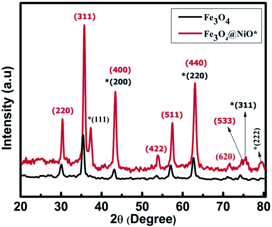
The crystal structures and phase purity of bare core and CS samples were examined and confirmed using an X-ray diffractometer (XRD, Rigaku, ULTIMA IV) containing Cu-Kα radiation in a 2θ range from 20° to 80°, as shown in Fig. 1. All corresponding peaks for NiO (JCPDS card no. 78-0643) and Fe3O4 (JCPDS card no. 89-3854) were indexed and both samples endorsed an fcc structure with the Fm![[3 with combining macron]](https://www.rsc.org/images/entities/char_0033_0304.gif) m space group with no other extra impurity peak visible in the XRD pattern of as-prepared MNPs. The average crystallite size for the bare core was found to be 24.58 nm, while for the CS sample, the shell material N confirmed an average crystallite size of 21.75 nm and the same for the core material was 23.43 nm using the scherrer formula.19,20 The lattice constant obtained for the bare core of FO was 8.39 Å, which is in total agreement with the recorded bulk value.21 However, the reduction of lattice constant is evident in the case of CS FO@N exhibiting a value of 8.31 Å. The probable reason for this effect might be mainly due to dissimilarities in the ionic radii of two materials,22,23 leading to a shift in the diffraction peak, as evident in CS FO@N XRD peaks displayed in Fig. 1.
m space group with no other extra impurity peak visible in the XRD pattern of as-prepared MNPs. The average crystallite size for the bare core was found to be 24.58 nm, while for the CS sample, the shell material N confirmed an average crystallite size of 21.75 nm and the same for the core material was 23.43 nm using the scherrer formula.19,20 The lattice constant obtained for the bare core of FO was 8.39 Å, which is in total agreement with the recorded bulk value.21 However, the reduction of lattice constant is evident in the case of CS FO@N exhibiting a value of 8.31 Å. The probable reason for this effect might be mainly due to dissimilarities in the ionic radii of two materials,22,23 leading to a shift in the diffraction peak, as evident in CS FO@N XRD peaks displayed in Fig. 1.
 |
| | Fig. 1 XRD spectrum of bare FO and CS FO@N. | |
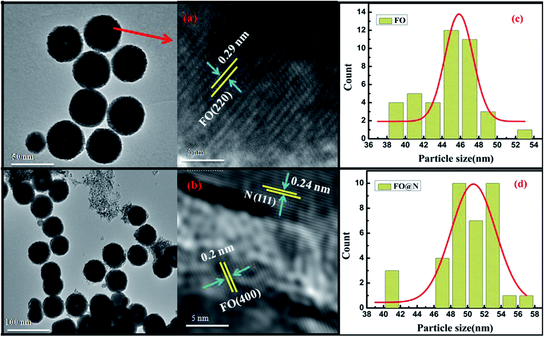
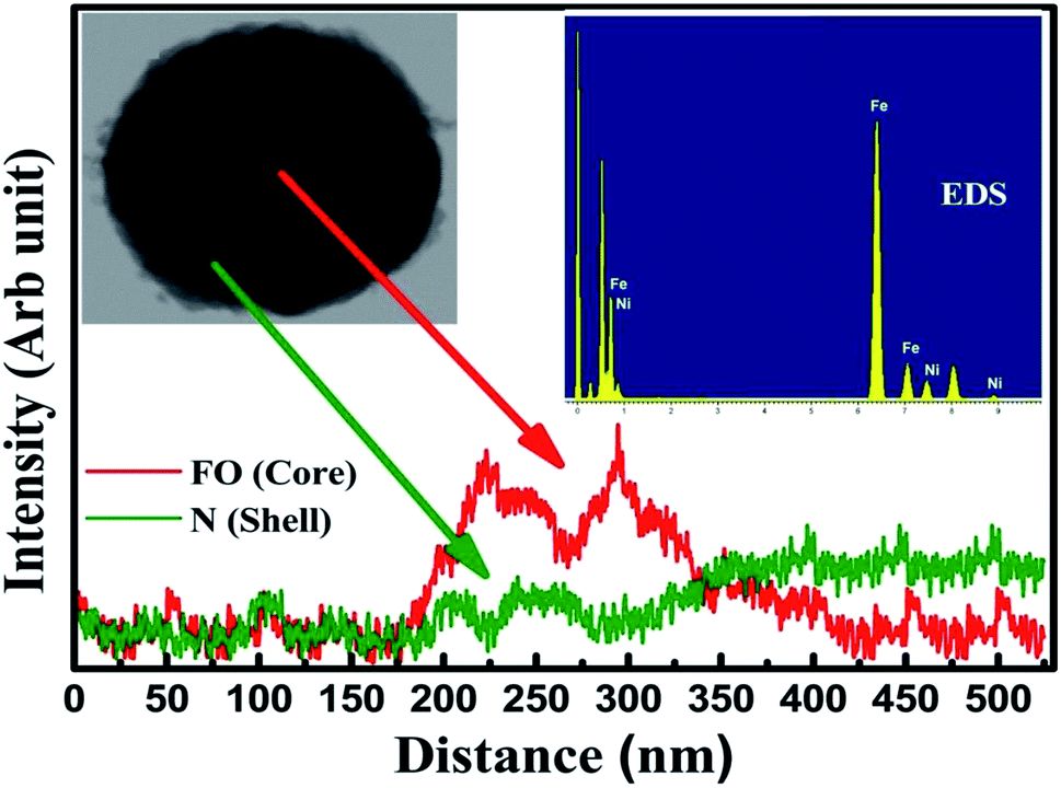
The morphology and particle size determination were performed using high-resolution transmission electron microscopy (HRTEM), model JEM 2100 of the JEOL make and endorses a uniform distribution of spherical nanoparticles, as shown in Fig. 2(a) and (b), where the displayed image confirmed the formation of the CS structure (Fig. 2b). The high-resolution image authenticates lattice fringes of 0.29 nm characteristic of the (220) plane for the bare core spinel, while the nanocomposite CS sample manifests the co-existence of both N and FO displaying lattice fringes of the (111) plane of 0.24 nm for the N shell and 0.20 nm of the (440) plane for the same core (FO) material. Fig. 2(c) and (d) displays the histograms of lognormal fits for both samples and extracted mean particle sizes were 45.34 nm and 50.17 nm for FO and FO@N, respectively. A slightly higher particle size prevailed for the CS nanostructure. A significant number of NPs in the TEM image were used to calculate the average shell dimension, which was found to be 3.69 nm. To further confirm the CS nanostructure, the elemental line mapping profile depicted in Fig. 3 was carefully analyzed for both core and shell materials. The line mapping profile, which authenticated FO at the center and N on the edge of NPs and the inset EDS elemental mapping shown in Fig. 3 clearly endorsed the CS nanostructure formation.
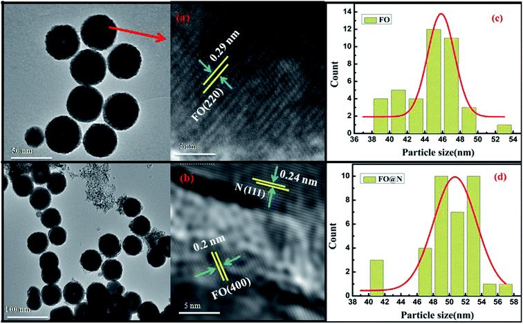 |
| | Fig. 2 (a and b) HRTEM images of FO and FO@N and (c and d) the particle size distribution of FO and FO@N respectively. | |
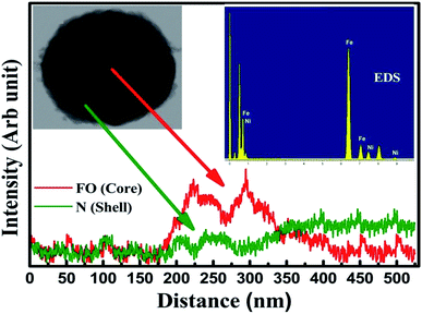 |
| | Fig. 3 Line mapping with the inset EDS of CS FO@N NPs. | |
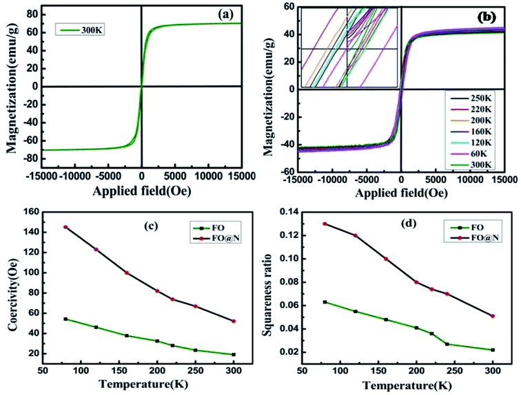
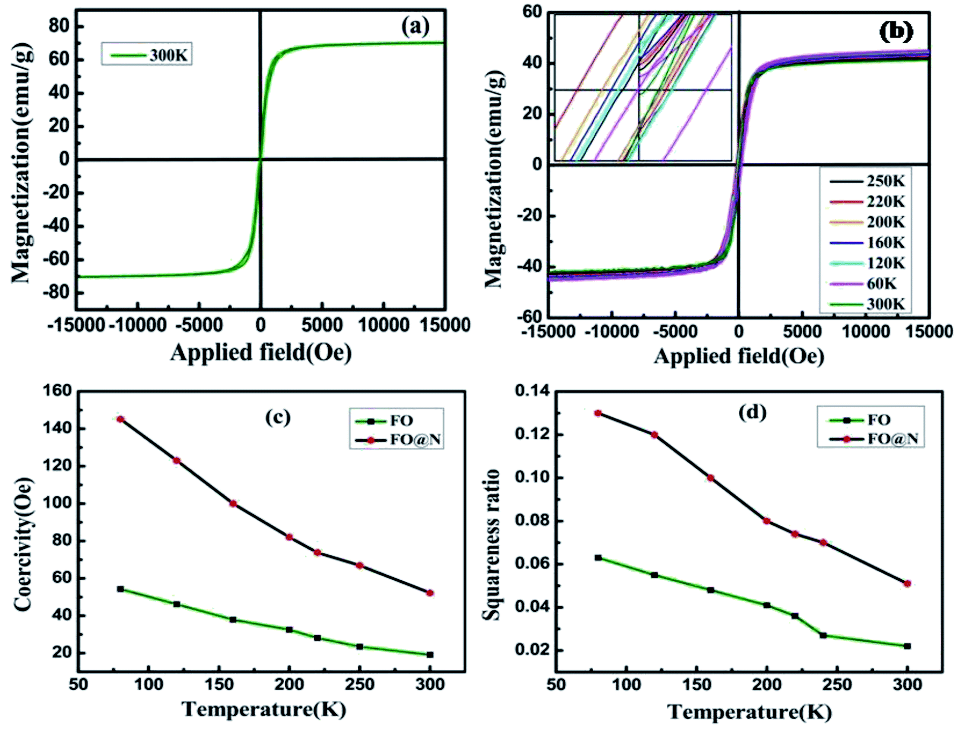
The magnetic measurement of both samples (FO and FO@N) was performed using a Lakeshore 7410 vibrating sample magnetometer (VSM), as displayed in Fig. 4(a) and (b). Room temperature saturation magnetization for the bare core FO was 69.87 emu g−1 and that of CS FO@N attained was 41.77 emu g−1. The shell material N gave an antiferromagnetic contribution to the core material, exhibiting a reduction in the net saturation magnetization of the CS sample. The M–H loop for the different temperatures of CS FO@N, which unveils a shifting of the hysteresis loop opposite to the direction of applied field is displayed in Fig. 4b, exhibiting both negative and positive EBE with respect to the temperature under field cooling conditions. At room temperature, EBE is not observed for the system; however, as the temperature reduces, the M–H loop starts to shift away from the center manifesting a negative EB field at 250 K. With a further decrease in temperature, the CS sample exhibited a maximum negative EB field HEB = −54.23 Oe at 220 K; interestingly, below 220 K, a reverse shifting of the M–H loop was encountered towards the center, displaying a lower negative EB field and the M–H loop shifting switched to positive EBE at around 180 K attributing to a characteristic switching temperature (Ts). Below Ts, positive EBE kept increasing and attained its maximum value of HEB = +101.63 Oe at 60 K. Despite the raising and lowering of EB field and the switching of EBE from negative to positive with descending temperature, the coercivity maintained a higher sequence of increment on lowering the temperature. The EB field HEB, coercivity Hc, saturation magnetization Ms, and squareness ratio Mr/Ms for all temperatures are given in Table 1.
 |
| | Fig. 4 (a and b) magnetization versus the applied field loop for FO and FO@N and (c and d) coercivity and the squareness ratio versus temperature graph. | |
Table 1 HEB, Hc, Ms, and Mr/Ms values of CS FO@N NPs for temperatures
| Temperature (K) |
HEB (Oe) |
Hc (Oe) |
Ms (emu g−1) |
Mr/Ms |
| 300 |
— |
52.19 |
41.77 |
0.051 |
| 250 |
−16.68 |
66.89 |
42.90 |
0.070 |
| 220 |
−54.23 |
73.79 |
43.29 |
0.074 |
| 200 |
−13.35 |
82.09 |
43.65 |
0.080 |
| 160 |
+11.49 |
100.23 |
44.29 |
0.10 |
| 120 |
+32.66 |
123.11 |
44.80 |
0.12 |
| 60 |
+101.63 |
146.18 |
45.18 |
0.13 |
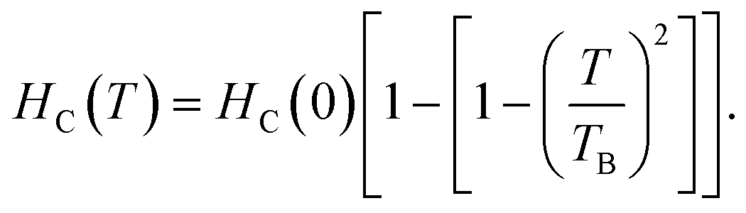
Fig. 4(c) and (d) display the coercivity and squareness ratio graph with temperature for CS FO@N in comparison to that of the bare FO sample. As shown in the figure, a strong FiM–AFM interface coupling is evident for CS FO@N displaying a larger harness as both the coercivity and squareness ratio are much higher compared to those of a single bare FO sample.10,24 The EB field (HEB) and coercivity (HC) of samples were extracted from the hysteresis loop of magnetization using formulas: HEB = (HC1 + HC2)/2 and HC = (HC1 − HC2)/2, where HC1 and HC2 represent the coercive fields of the left and right branches of M–H loops along with their sign, respectively. The switching of EBE from negative to positive for the NP system was first reported by Ihab et al. for the FiM–FiM CS nanostructure. Moreover, in their report, the switching was encountered for increasing temperature and different cooling fields.16 Our result shows a different trend as the EBE switching from negative to positive is completely a temperature-dependent phenomenon at a fixed intermediate cooling field. The observation of negative EBE at 250 K is usual; however, the existence of positive EBE at lower temperatures below 160 K is novel, and this type of characteristic switching has not been reported for a fixed cooling field to the best of our knowledge, especially for the FiM/AFM nanoparticle CS system. Usually, in a system with the CS nanostructure, an intrinsic surface effect is encountered causing a magnetic disorder, which consequently produces uncompensated spins at the interface.25,26 When the system is examined under field cooling conditions, the anisotropy of AFM is expected to be modified due to the interface effect of the FiM/AFM system, and essentially, uncompensated spins at the interface are either pinned or unpinned with respect to FiM spins.27 Therefore, the consequence of the shift in hysteresis loop and the amplification of the coercive field are expected to originate from the pinned and unpinned uncompensated spins of AFM at the magnetically disordered interface. When the sample is under field cooling, unpinned spins are dragged and rotate along the field direction providing an extra magnetization to FiM, which leads to the coercivity enhancement. However, uncompensated spins, which are pinned with FiM spins at the interface will require a larger field to rotate and remain fixed during magnetization reversal, favouring a shift in the hysteresis loop, resulting in EBE. It is worth noting that the usual emergence of positive exchange bias is a consequence of the applied high cooling field. However, for an intermediate or low cooling field, the occurrence of EBE (either positive or negative) has a complex dependence on the sign of interface coupling spins and their coupling magnitude. EBE is totally a temperature-dependent phenomenon and usually disappears above the blocking temperature (TB). In our CS system, EBE is not evident at room temperature as the blocking temperature of the CS sample is below the room temperature (approximately around 289 K). The blocking temperature of the sample is extracted from the coercivity dependence on temperature using the equation28  Below the blocking temperature, AFM uncompensated spins at the interface preferred a ferromagnetic arrangement with core FiM spins, where uncompensated spins are strongly coupled due to their high anisotropy and remain fixed during the reversal, exhibiting the usual negative EBE. With a further decrease of temperature, the effective interfacial ferromagnetic coupling is hindered and temperature-dependent phase transition is attained around 180 K. Below this switching temperature, on field cooling, an unstable domain is expected to be created at the AFM layer and as a consequence leads to a mixture of frustrated coupling and antiferromagnetically satisfied interface interaction, where the antiferromagnetic coupling will be significant. Therefore, below this characteristic switching temperature, this AFM dominant region will lead to a significant sign reversal and consequently, EBE switches from negative to positive direction. At higher temperatures, the thermal energy is high enough to suppress domains in the AFM layer and they suddenly disappear at the switching temperature following a parallel interfacial coupling, leading to the usual negative EBE and disappear at the blocking temperature. Therefore, the temperature-dependent switching of EBE from negative to positive has possibly originated from the ferromagnetic or antiferromagnetic coupling at the magnetically disordered FiM/AFM interface. The schematic on the arrangement of spins concerning the interface of core–shell and the said EB switching mechanism is depicted in Fig. 5.
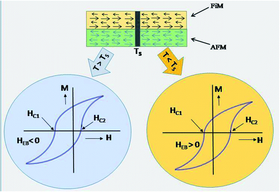 |
| | Fig. 5 Schematic representation on the mechanism of negative and positive EBE. | |
Conclusion
A FO@N CS nanostructure is prepared using a two step co-precipitation method. The phase purity and crystal structure were analyzed and confirmed through the XRD study. The formation of CS nanostructure is authenticated through HRTEM and elemental line mapping with EDS, which followed the XRD analysis. The magnetic measurement of CS sample under fixed field cooling conditions exhibited a novel characteristic as the shifting of the hysteresis loop (EBE) switched from negative to positive direction with a decrease in the temperature. The switching of EBE from negative to positive direction with temperature is expected to originate from the ferromagnetic or antiferromagnetic coupling of spins at the FiM/AFM magnetic interface.
Author contributions
S. P. Tsopoe and J. P. Borah prepared the sample and they have done most of the analysis and characterizations of the work. They have also written most of the portion of the manuscript. C. Borgohain has done magnetic measurement and HRTEM characterization. All the authors have reviewed and verified the manuscript.
Conflicts of interest
There are no conflicts to declare.
Acknowledgements
The authors would like to acknowledge the Central Instrumentation Facility (CIF), Indian Institute of Technology Guwahati, Guwahati 781039, India for granting access to the available instrument facilities.
References
- J. Nogués and I. K. Schuller, J. Magn. Magn. Mater., 1999, 192, 203–232 CrossRef
 .
. - W. H. Meiklejohn and C. P. Bean, Phys. Rev., 1956, 102, 1413–1414 CrossRef .
- C. Borgohain, D. Mishra, K. C. Sarma and P. Phukan, J. Appl. Phys., 2012, 112, 2–7 CrossRef .
- I. Obaidat, C. Nayek, K. Manna, G. Bhattacharjee, I. Al-Omari and A. Gismelseed, Nanomaterials, 2017, 7, 415 CrossRef PubMed .
- X. He, Y. Xu, X. Yao, C. Zhang, Y. Pu, X. Wang, W. Mao, Y. Du and W. Zhong, RSC Adv., 2019, 9, 30195–30206 RSC .
- E. Lottini, A. López-Ortega, G. Bertoni, S. Turner, M. Meledina, G. Van Tendeloo, C. De Julián Fernández and C. Sangregorio, Chem. Mater., 2016, 28, 4214–4222 CrossRef CAS .
- S. M. Yusuf, P. K. Manna, M. M. Shirolkar, S. K. Kulkarni, R. Tewari and G. K. Dey, J. Appl. Phys., 2013, 113, 1–6 CrossRef .
- S. Y. Yin, S. L. Yuan, Z. M. Tian, C. H. Wang, S. X. Huo, H. N. Duan, X. F. Zheng and K. L. Liu, J. Appl. Phys., 2010, 107(7), 073915 CrossRef .
- J. Ventura, J. P. Araujo, J. B. Sousa, A. Veloso and P. P. Freitas, Phys. Rev. B: Condens. Matter Mater. Phys., 2008, 77, 1–8 CrossRef .
- S. P. Tsopoe, C. Borgohain, R. Fopase, L. M. Pandey and J. P. Borah, Sci. Rep., 2020, 10, 1–15 CrossRef PubMed .
- S. Anandakumar, V. S. Rani, S. Oh and C. Kim, Thin Solid Films, 2010, 519, 1020–1024 CrossRef CAS .
- N. N. Phuoc, N. P. Thuy, N. A. Tuan, L. T. Hung, N. T. Thanh and N. T. Nam, J. Magn. Magn. Mater., 2006, 298, 43–47 CrossRef CAS .
- J. Nogués, D. Lederman, T. J. Moran and I. K. Schuller, Phys. Rev. Lett., 1996, 76, 4624–4627 CrossRef PubMed .
- I. V. Roshchin, O. Petracic, R. Morales, Z. P. Li, X. Batlle and I. K. Schuller, Europhys. Lett., 2005, 71, 297–303 CrossRef CAS .
- H. Shi, D. Lederman, N. R. Dilley, R. C. Black, J. Diedrichs, K. Jensen and M. B. Simmonds, J. Appl. Phys., 2003, 93, 8600–8602 CrossRef CAS .
- I. M. Obaidat, C. Nayek, K. Manna, G. Bhattacharjee, I. A. Al-Omari and A. Gismelseed, Nanomaterials, 2017, 7(12), 415 CrossRef PubMed .
- Y. A. A. Rahdar and M. Aliahmad, J. Nanostruct., 2015, 1–7 Search PubMed .
- A. Fadli, Komalasari, A. Adnan, Iwantono, Rahimah and A. S. Addabsi, IOP Conf. Ser.: Mater. Sci. Eng., 2019, 622, 012013 CAS .
- A. L. Patterson, Phys. Rev., 1939, 56, 978–982 CrossRef CAS .
- P. Seal, N. Paul, P. D. Babu and J. P. Borah, Appl. Phys. A: Mater. Sci. Process., 2019, 125, 1–9 CrossRef .
- S. H. Chaki, T. J. Malek, M. D. Chaudhary, J. P. Tailor and M. P. Deshpande, Adv. Nat. Sci.: Nanosci. Nanotechnol., 2015, 6, 035009 Search PubMed .
- L. Chen, P. Fleming, V. Morris, J. D. Holmes and M. A. Morris, J. Phys. Chem. C, 2010, 12909–12919 CrossRef CAS .
- J. T. L. Gamler, A. Leonardi, X. Sang, K. M. Koczkur, R. R. Unocic, M. Engel and S. E. Skrabalak, Nanoscale Adv., 2020, 3(2), 1105–1114 RSC .
- E. Lima, E. L. Winkler, D. Tobia, H. E. Troiani, R. D. Zysler, E. Agostinelli and D. Fiorani, Chem. Mater., 2012, 24, 512–516 CrossRef CAS .
- A. L. Source, O. C. Road and L. Berkeley, 2003, 2–5.
- J. A. González, J. P. Andrés, R. López Antón, J. A. De Toro, P. S. Normile, P. Muñiz, J. M. Riveiro and J. Nogués, Chem. Mater., 2017, 29, 5200–5206 CrossRef .
- A. Sahoo, D. Bhattacharya and P. K. Mohanty, Phys. Rev. B, 2020, 101, 064414 CrossRef CAS .
- K. Maaz, A. Mumtaz, S. K. Hasanain and M. F. Bertino, J. Magn. Magn. Mater., 2010, 322, 2199–2202 CrossRef CAS .
|
| This journal is © The Royal Society of Chemistry 2021 |
Click here to see how this site uses Cookies. View our privacy policy here. 
 Open Access Article
 This Open Access Article is licensed under a Creative Commons Attribution-Non Commercial 3.0 Unported Licence
 *a
*a
 Below the blocking temperature, AFM uncompensated spins at the interface preferred a ferromagnetic arrangement with core FiM spins, where uncompensated spins are strongly coupled due to their high anisotropy and remain fixed during the reversal, exhibiting the usual negative EBE. With a further decrease of temperature, the effective interfacial ferromagnetic coupling is hindered and temperature-dependent phase transition is attained around 180 K. Below this switching temperature, on field cooling, an unstable domain is expected to be created at the AFM layer and as a consequence leads to a mixture of frustrated coupling and antiferromagnetically satisfied interface interaction, where the antiferromagnetic coupling will be significant. Therefore, below this characteristic switching temperature, this AFM dominant region will lead to a significant sign reversal and consequently, EBE switches from negative to positive direction. At higher temperatures, the thermal energy is high enough to suppress domains in the AFM layer and they suddenly disappear at the switching temperature following a parallel interfacial coupling, leading to the usual negative EBE and disappear at the blocking temperature. Therefore, the temperature-dependent switching of EBE from negative to positive has possibly originated from the ferromagnetic or antiferromagnetic coupling at the magnetically disordered FiM/AFM interface. The schematic on the arrangement of spins concerning the interface of core–shell and the said EB switching mechanism is depicted in Fig. 5.