
 Open Access Article
 This Open Access Article is licensed under a Creative Commons Attribution-Non Commercial 3.0 Unported Licence
The recombination zone adjusted by the gradient doping of TPA-DCPP for efficient and stable deep red organic light emitting diodes†
Qianmin Zhanga,
Jixin Jianga,
Zheng Xua,
Dandan Song a,
Bo Qiaoa,
Suling Zhao*ab,
S. Wagehb and
Ahmed Al-Ghamdib
a,
Bo Qiaoa,
Suling Zhao*ab,
S. Wagehb and
Ahmed Al-Ghamdib
aKey Laboratory of Luminescence and Optical Information, Beijing Jiaotong University, Ministry of Education, Beijing 100044, China. E-mail: slzhao@bjtu.edu.cn
bDepartment of Physics, Faculty of Science, King Abdulaziz University, Jeddah 21589, Saudi Arabia
First published on 13th July 2021
Abstract
Deep-red organic light-emitting diodes (DR-OLEDs) or near-infrared organic light-emitting diodes (NIR-OLEDs) have a wide range of applications in real life, such as special light sources for plant growth in agriculture, optical communications, infrared imaging, infrared medical imaging and other fields. However, the device performance of DR-OLEDs is still far behind that of red, green and blue OLEDs. In addition to the well-known energy gap law, the location of the recombination region also has a significant impact on the device performance. If the recombination area is too close to the cathode, the electrons in the electron transport layer will easily cause exciton quenching. In this study, for the first time, we adopted a quantum well-like structure by changing the host (CBP) and guest (TPA-DCPP) thicknesses as the light-emitting layer to manage the position of the recombination zone, and then improved the carrier injection and transportation as well as increased the exciton recombination rate. Furthermore, we introduced a hole trap layer to reduce the current density and suppress the recombination zone movement; finally, we prepared high-brightness and high-efficiency DR-OLEDs based on the TADF material with a wavelength of 674 nm, a maximum brightness of 1151 cd m−2 and a maximum EQE of 4.4%.
Introduction
With the development of economy and technology, increasingly demanding display quality is required.1–6 At present, organic light-emitting diodes (OLEDs) are a widely used display technology since their invention by Tang and VanSlyke in 1987.7 After decades of effort, luminescent materials evolved from the original fluorescent emitters to the current phosphorescent emitters and thermally activated delayed fluorescent (TADF) emitters. The latter of these emitters break the spin statistics of electron transition as known as phosphorescent OLEDs (PhOLEDs) and thermally activated delayed fluorescent OLEDs (TADF-OLEDs) with the internal quantum efficiency (IQE) as high as 100% theoretically,8–10 in which TADF emitters are more favored because they do not need heavy metals and are environmentally friendly.11,12Although red, green and blue organic light-emitting diodes (OLEDs) already have achieved their high efficiency and have been widely used, the development of DR-OLEDs (λmax: 650 nm to 750 nm) or even NIR-OLEDs is still very slow due to three main reasons:13,14 the first is the well-known energy gap law.15 When the energy gap of the emitter decreases, the nonradiative decay rate increases. Correspondingly, DR-OLEDs or NIR-OLEDs are always accompanied by a lower efficiency compared to others.16–18 Besides the energy gap law, the second reason is that in traditional host–guest-doped devices, the exciton recombination region is narrow and the exciton interaction easily triggers quenching, such as singlet/triplet–triplet annihilation.19–21 The last reason is the imbalance in the carrier injection and transportation: too many holes or electrons are not conducive to improve the luminous efficiency of devices.22–26 Therefore, most researchers focus on these three aspects to study how to improve the efficiency of DR-OLEDs or even NIR-OLEDs. Recently, Chen et al.15 reported a novel red TADF emitter, namely 10-(11,12-di(pyridin-3-yl)dibenzo[a,c]phenazin-3-yl)-10H-phenoxazine(mDPBPZ-PXZ). mDPBPZ-PXZ releases two pyridine substituents out of its fused acceptor moiety as a steric hindrance to suppress intermolecular π–π interactions and shows a very high photoluminescence quantum yield (ΦPL) of 95 ± 1.3%. Its non-doped device shows a superior maximum external quantum efficiency (EQEmax) of 5.2% with deep red/NIR emission at a peak of 680 nm. Shen et al.17 studied the role of an ancillary acceptor of cyanophenyl. They designed and synthesized a new D–A type molecule, namely 4-(7-(4-(diphenylamino)phenyl)-9-oxo-9H-fluoren-2-yl)benzonitrile (TPA-FOCN), by introducing cyanophenyl, which not only shifts the emission of TPA-FOCN to the deep red region with a peak of 668 nm in solid, but also maintains a high ΦPL of 10%. Finally, an EQEmax of 0.22% with Commission Internationale de l'Eclairage (CIE) coordinates of (0.64, 0.35) in its non-doped device was realized. It is a meaningful attempt for non-doped solution-processed DR-OLEDs, even though its EQE fails to meet the expectations. In terms of structure improvement, in 2017, Li et al.27 combined the interface exciplex with a multi quantum well structure, and formed a series of quantum well structures by alternately inserting TCTA and B3PYMPM, and finally achieved extremely low efficiency roll-off in green OLEDs. In 2014, Lee et al.20 introduced charge control layers on the basis of the traditional quantum well structure, that is, a mixed layer of mcp and TPBi was inserted into the two quantum wells to achieve a distributed recombination zone and a balanced charge carrier injection, which eventually increased the lifetime of the blue phosphorescent organic light emitting diodes by 3.5 times. It can be seen that the existing improvement methods need to introduce additional functional layers or more steps, which is not conducive to save time and cost.
In this study, the efficiency of DR-OLEDs based on the red TADF material TPA-DCPP was improved by designing a device structure. TPA-DCPP is one of the few commercial materials in the deep red region. The existing research is in the form of host–guest doping,28–30 which not only increases the difficulty of the experiment but also reduces the repeatability of the experiment. Moreover, the narrow recombination zone is not conducive to improve the device performance. Although the traditional quantum well structure avoids the above-mentioned problems, it does not consider the balanced carrier injection. Therefore, it is necessary to create an improved quantum well structure as the emitting light layer to adjust the performance of TPA-DCPP OLEDs. First, we adopted a quantum well-like structure as the light-emitting layer, and the introduction of a quantum well structure could broaden the exciton recombination area and reduce the exciton quenching. Second, considering the imbalance of the carrier transportation, we reduced the thickness of the host and guest layer to adjust the hole–electron recombination regain, and improved the luminous efficiency. Third, in order to reduce the current density, a hole trap layer was introduced. Finally, we successfully achieved highly efficient and stable deep red OLEDs in a host–guest non-doped form with a light emission wavelength of 674 nm, a maximum brightness (Lmax) of 1151 cd m−2, and EQEmax of 4.4%.
Experimental
In this study, 4,40-bis(9-carbazolyl)-1,10-biphenyl (CBP) was used as the host material due to its good bipolar transport characteristics and 7,10-bis(4-(diphenylamino)phenyl)-2,3-dicyanopyrazino phenanthrene (TPA-DCPP) was used as the guest material. Molybdenum(VI) oxide (MoO3) and N,N′-bis(naphthalen-1-yl)-N,N′-bis(phenyl)-benzidine(NPB) were used as the hole injection and transport layers, respectively. 4,7-Diphenyl-1,10-phenanthroline (Bphen) was used as the electron transport layer. Lithium fluoride (LiF) was used as the cathode modification material, which could improve the work function, and Al was the cathode. TPA-DCPP was purchased from Lumtec company, and other materials were purchased from Xi'an p-OLED Optoelectronics Technology Co. Ltd. The molecular structures of NPB, CBP, TPA-DCPP and Bphen are shown in Fig. 1.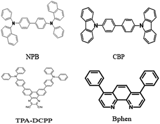 | ||
| Fig. 1 The molecular structures of the materials used, which are NPB, CBP, TPA-DCPP and Bphen. | ||
ITO-coated glasses used as the anode in all devices were treated with alcohol, deionized water, and oxygen plasma to remove surface defects before depositing films. The film thickness and evaporation rate were monitored by a quartz crystal. The evaporation rate of organic materials was 0.3–0.5 Å s−1, and the evaporation rate of inorganic materials was 1–2 Å s−1. The light-emitting layers were deposited by co-heating and cross evaporating. At first, the sources of CBP and TPA-DCPP were co-heated to the evaporation temperature. Then, CBP, TPA-DCPP, and CBP were deposited in turn to form the non-doped structure. In this way, a flat and dense film could be obtained. All films were prepared under a pressure of below 1 × 10⁻⁴ Pa. The specific experimental process is shown in the ESI.†
The current–voltage–luminance (J–V–L) characteristics and electroluminescence (EL) spectrum of DR-OLEDs were measured by a Keithley 2410 source and an SRC-600 spectral radiance colorimeter. All measurements were made under air conditions.
Results and discussion
First, a series of non-doped TADF-OLEDs were studied with the same structure, as shown in Fig. 2, except for the different emitting layers (EML) as: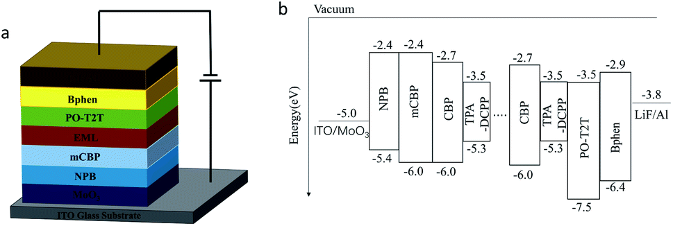 | ||
| Fig. 2 (a) Device structure of the OLEDs and (b) energy level diagram of the OLEDs. | ||
Devices A1–A6:
| ITO/MoO3 (5 nm)/NPB (33 nm)/EML/Bphen (45 nm)/LiF (0.5 nm)/Al (100 nm) |
The light performances of A devices were detected, as shown in Fig. 3. When the number n of QWs decreased from n = 12 to n = 2, correspondingly, the thickness of each guest layer increased from 1 nm to 6 nm, and each host layer increased from 2.5 nm to 15 nm, the EL peak red-shifted from 660 nm to 697 nm due to the enhanced interaction between the guest molecules. It is worth mentioning that all devices exhibited deep red light, and only one emission peak came from TPA-DCPP, as shown in Fig. 3a, indicating the stable light emission and the sufficient energy transfer from CBP to TPA-DCPP. Fig. 3b shows the current–voltage–luminance (J–V–L) characteristics of all devices. As the number of QWs increased from 2 to 6, the current density increased with the QW numbers at the same driving voltage. It was because the thickness of each CBP and TPA-DCPP layer in the EML decreased along with the increase in n, which greatly promoted the carriers transporting through TPA-DCPP with a relatively poor carrier transportation ability compared with CBP. At low current density, as shown in Fig. 3c, the luminous efficiency increased slowly with the current density, particularly for the device with 6 QWs, which showed a typical trap-assisted recombination mechanism. Then, EQE reached the maximum slower for increasing n, at which the traps or defects were filled fully by carriers due to the increasing traps inside the devices, as shown in Fig. 3c. Therefore, it was concluded that the trap or defect density increased along with the increase n, due the introduction of the CBP/TPA-DCPP interface increasing when the QW number was lower than 6.
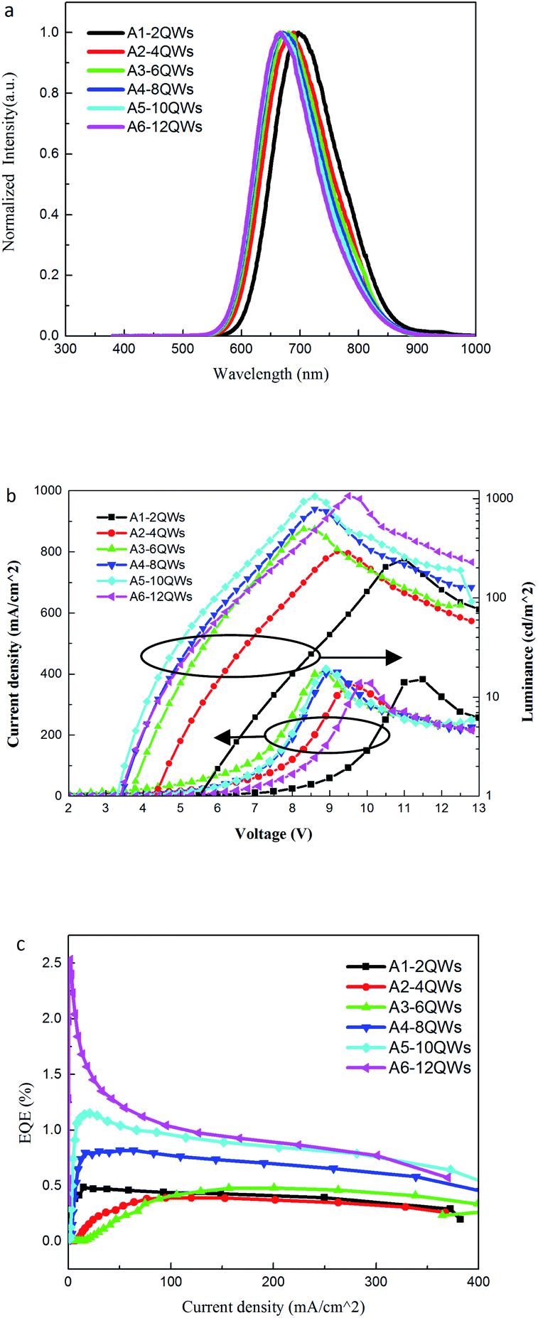 | ||
| Fig. 3 (a) Normalized electroluminescence spectra of the DR-OLEDs. (b) Current–voltage–luminance (J–V–L) of OLEDs based on various QW units. (c) External quantum efficiency of OLEDs based on various QW units. | ||
When the number of QWs exceeds 6, the CBP/TPA-DCPP interface inside EML and the confinement effect on carriers due the thinner thickness increase; therefore, the current density gradually decreases as n increases. Conversely, the electroluminescence efficiency increases sharply at low current density then decrease, which shows a trend to the direct electron–hole recombination characteristics on TPA-DCPP layer even there are more traps or defects from CBP/TPA-DCPP interfaces. The thinner per CBP and TPA-DCPP layer along with the increase n helped to increase carrier tunneling probability. In such case, more electrons and holes were injected to TPA-DCPP, and recombined directly to emit. Under the same voltage, the luminance increased with the number of quantum wells, and the maximum luminance occurred when n = 10, which was 1053 cd m−2. More the quantum wells are, more the homogeneous distribution of TPA-DCPP in whole EML is, and the weaker the exciton interaction is, which can be concluded from the blue-shift of the EL peak along with the increase in n. Therefore, the efficiency enhanced, and EQEmax was 2.53% when n = 12; however, its efficiency roll-off was also very serious.
In OLED devices, the position of the recombination area plays a decisive role in improving the performance of the device. If the position of the recombination area is close to the cathode, excitons quench easily through interaction with traps from the cathode interface and polarons from the unbalanced carriers. On the other hand, some emitted photons will be re-absorbed by TPA-DCPP layers on the light out way, if the recombination area is too far away from the anode. Therefore, the device performance decreases. Hence, we introduced a sensing layer to explore the position of the recombination area and choose Ir(ppy)3, a green phosphorescent material with a peak wavelength of 529 nm as the sensing layer to replace one TPA-DCPP layer in the light-emitting layer, and prepared devices B1–B6. Then, analyzed whether there was green light in the spectrum to study the location of the recombination area. The experimental process and results are shown in the ESI.† It can be seen from the ESI† that only when Ir(ppy)3 replaced the last layer of TPA-DCPP, there was a weak luminescence at 529 nm in the spectrum of device B6, indicating that the recombination area was close to the electron transport layer side because Ir(ppy)3 had a wider energy gap than TPA-DCPP. Only electrons and holes met each other in this region where Ir(ppy)3 was located, and Ir(ppy)3 could emit. Therefore, in order to improve the performance of the devices, it is necessary to adjust the position of the recombination area moving far from the cathode.
In above experiments, the thickness of each TPA-DCPP layer and CBP layer was the same inside the EML. Considering that the electron mobility of TPA-DCPP is very low, its thickness has a great influence on the injection and transportation of electrons, and thus, the recombination area. CBP is a unipolar host material, and its hole transport ability is higher than that of electron (μh = 2.1 × 10⁻³ cm2 V−1 s−1, μe = 0.45 × 10⁻³ cm2 V−1 s−1),31 so its thickness affects the electron injection. In addition, the exciton formation zone is narrow to quench easily; therefore, we changed the thickness of each TPA-DCPP layer to adjust the position of the recombination area, then prepared device C with the same structure as device A5, but with different EML, and the exciton blocking layer PO-T2T was introduced as follows.
The whole thickness of the guest material TPA-DCPP is 12 nm, and each TPA-DCPP layer in QWs was changed as the increasing or decreasing gradient doping to adjust the recombination area. The performance of three devices is depicted in Fig. 4. When the thickness of the guest changing, the emission wavelength red-shifts to 680 nm in device C1, and blue-shifts to 652 nm in device C2 compared to device A5. Without changing any conditions, the shift of the emission wavelength came from the change in the recombination area. The longer wavelength corresponds to the emission from the thicker TPA-DCPP layer in EML, and the shorter wavelength emission corresponds to the thinner TPA-DCPP layer. It suggests further that the recombination area is close to the electron transport layer. When the thickness of the guest on the side of the electron transport layer changed from large to small, the guest molecule interaction was reduced, so the wavelength blue shifted. The change in brightness and efficiency is the same. When the thickness of the guest near the electron transport layer is the largest, Lmax is 931 cd m−2 and EQEmax is 2.7%. When the thickness of the guest near the electron transport layer is the smallest, Lmax is 2237 cd m−2 and EQEmax is 4.7%. The turn on voltages of the three C devices remained almost unchanged. The brightness and efficiency of the C2 device have been greatly improved, indicating that we have used gradient doping to change the position of the recombination region and reduced the quenching of excitons by the electron transport layer, thus the device performance has been improved (Table 1).
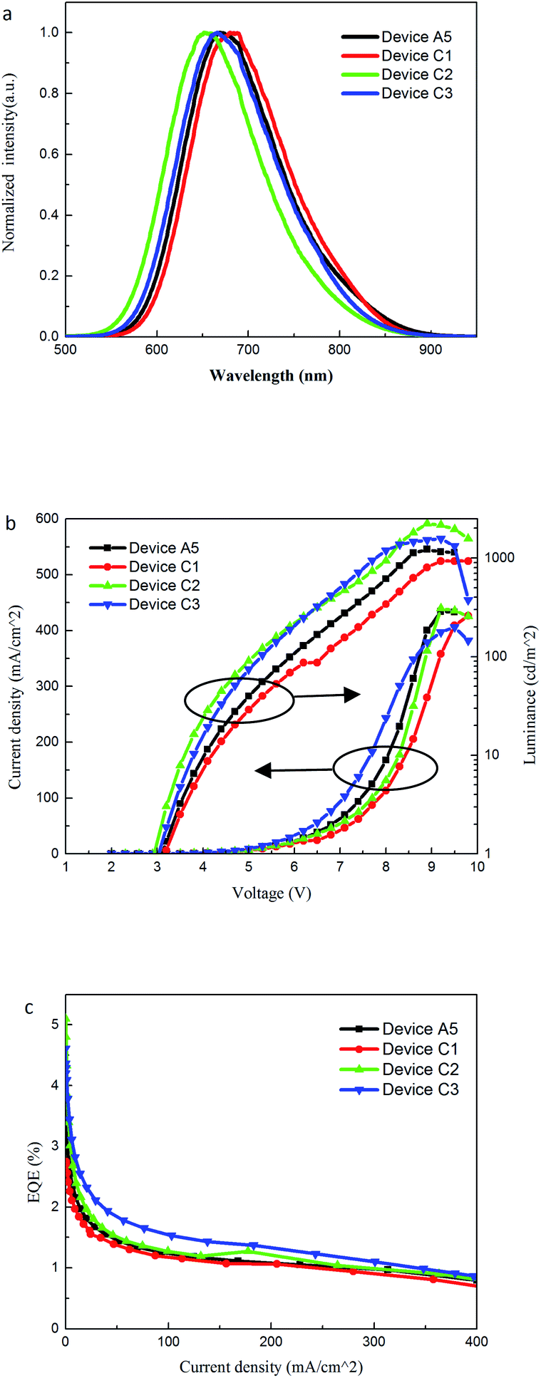 | ||
| Fig. 4 (a) Normalized electroluminescence spectra of DR-OLEDs. (b) Current–voltage–luminance (J–V–L) of OLEDs based on different thicknesses of the guest. (c) External quantum efficiency of OLEDs based on different thicknesses of the guest. | ||
| Device | Wavelength (nm) | Turn-on (V) | Lmax (cd m−2) | EQEmax (%) | EQEa (%) |
|---|---|---|---|---|---|
| a EQE at current density of 100 mA (cm2)−1. | |||||
| A5: [CBP (3 nm)/TPA-DCPP (1.2 nm)]10 | 669 | 3.2 | 1225 | 3.3 ± 0.1 | 1.2 ± 0.03 |
| C1: [CBP (3 nm)/TPA-DCPP (0.4 nm)]2/[CBP (3 nm)/TPA-DCPP (0.8 nm)]2/[CBP (3 nm)/TPA-DCPP (1.2 nm)]2/[CBP (3 nm)/TPA-DCPP (1.6 nm)]2/[CBP (3 nm)/TPA-DCPP (2 nm)]2 | 680 | 3.2 | 931 | 2.7 ± 0.1 | 1.2 ± 0.03 |
| C2: [CBP (3 nm)/TPA-DCPP (2 nm)]2/[CBP (3 nm)/TPA-DCPP (1.6 nm)]2/[CBP (3 nm)/TPA-DCPP (1.2 nm)]2/[CBP (3 nm)/TPA-DCPP (0.8 nm)]2/[CBP (3 nm)/TPA-DCPP (0.4 nm)]2 | 652 | 2.9 | 2237 | 4.7 ± 0.2 | 1.3 ± 0.01 |
| C3: [CBP (5 nm)/TPA-DCPP (2 nm)]2/[CBP (4 nm)/TPA-DCPP (1.6 nm)]2/[CBP (3 nm)/TPA-DCPP (1.2 nm)]2/[CBP (2 nm)/TPA-DCPP (0.8 nm)]2/[CBP (1 nm)/TPA-DCPP (0.4 nm)]2 | 669 | 3.1 | 1568 | 4.1 ± 0.2 | 1.5 ± 0.03 |
According to the above-mentioned results, we further changed the thickness of each CBP layer based on the structure of device C2 and prepared device C3 in order to adjust the recombination area and keep the EL peak in the deep red region. The emission peak of device C3 is same as that of device A5 at 669 nm, as shown in Fig. 4a, which is different to that of device C2; even the thickness configuration of TPA-DCPP in the two devices is the same. It shows that the recombination area of device C3 is different to device C2 and moves to the side of the anode. Also, device C3 has the maximum brightness, which is 1568 cd m−2 with the deep red emission at 669 nm. It can be concluded that when the thickness of CBP and TPA-DCPP near the cathode is reduced, the electron injection and transportation significantly increased. Under a high current density as 100 mA (cm2)−1, EQE of C3 is the biggest, which shows that C3 has a lower efficiency roll-off and more stable performance than others.
However, the current density of C devices was still large, and according to the above experiments the recombination zone was close to the cathode, we suspected that the holes were the majority carrier in all the devices, and the hole mobility is greater than the electron mobility. Therefore, we tried to reduce the hole current by introducing a hole trap layer between HTL and EML and adjust the recombination zone to the anode. 3,3′-Di(9H-carbazol-9-yl) biphenyl (mCBP) was used as the hole trap layer; then, we made series of devices with different mCBP thicknesses of 1 nm, 2 nm, 3 nm, 4 nm, and 5 nm. The energy level structure of the devices after the introduction of mCBP is shown in Fig. 2 with the same EML structure of device C3 as follows.
Devices D1-5:
| ITO/MoO3 (5 nm)/NPB (33 nm)/mCBP (X nm, X = 1, 2, 3, 4, 5)/[CBP (5 nm)/TPA-DCPP (2 nm)]2/[CBP (4 nm)/TPA-DCPP (1.6 nm)]2/[CBP (3 nm)/TPA-DCPP (1.2 nm)]2/[CBP (2 nm)/TPA-DCPP (0.8 nm)]2/[CBP (1 nm)/TPA-DCPP (0.4 nm)]2/PO-T2T (15 nm)/Bphen (45 nm)/LiF (1 nm)/Al (100 nm) |
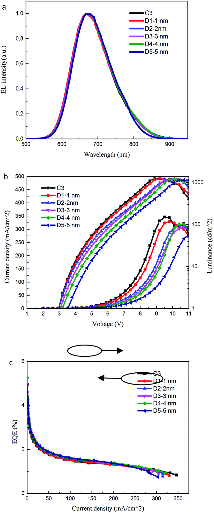
The device performance is shown in Fig. 5. As shown in Fig. 5a, when the driving voltage was 10 V, all D devices have only one electroluminescence peak coming from TPA-DCPP. Compared to the emission peak of C3 at 668 nm, when 4 nm/5 nm mCBP is introduced, the emission peak is 674 nm, and the little wavelength red-shift is due to the movement of the recombination region from the ETL side to the HTL side because the thickness of the guest is arranged from large to small in the light-emitting layer; therefore, the interaction between the guests is the largest near the HTL side. (Table 2) When the recombination region is near the HTL side, the wavelength red-shifted. From Fig. 5b, after the hole trap layer is introduced, the current density decreased significantly under the same voltage. As the thickness of the trap layer increases, the blocking effect on holes becomes stronger, and the current density decreased more significantly. Therefore, the resistance increases and the turn on voltage gradually increases from 3 V to 3.5 V. Even though the brightness decreases slightly due to the red-shift of the wavelength, the luminous efficiency increased from 3.9% to 4.4%, as shown in Fig. 5c, which was due to the movement of the recombination area and balanced two carriers by introducing the hole trap layer.
 | ||
| Fig. 5 (a) Normalized electroluminescence spectra of the DR-OLEDs. (b) Current–voltage–luminance (J–V–L) of OLEDs based on different thickness of mCBP. (c) External quantum efficiency of OLEDs based on different thickness of mCBP. | ||
| Device | Wavelength (nm) | Turn-on (V) | Lmax (cd m−2) | EQEmax (%) | EQEa (%) |
|---|---|---|---|---|---|
| a EQE at current density of 100 mA (cm2)−1. | |||||
| C3 | 668 | 3 | 1241 | 3.9 ± 0.1 | 1.4 ± 0.1 |
| D1 | 666 | 3 | 1249 | 3.9 ± 0.2 | 1.4 ± 0.1 |
| D2 | 668 | 3 | 1176 | 4.2 ± 0.1 | 1.5 ± 0.1 |
| D3 | 669 | 3.1 | 1232 | 4.2 ± 0.1 | 1.6 ± 0.1 |
| D4 | 674 | 3.2 | 1210 | 4.3 ± 0.1 | 1.6 ± 0.1 |
| D5 | 674 | 3.5 | 1151 | 4.4 ± 0.1 | 1.8 ± 0.5 |
Conclusions
We adopted a quantum well (QW)-like structure as the light-emitting layer, and changed the thickness of the host and guest to adjust the position of the recombination zone; besides, we introduced a hole trap layer to reduce the current density, and successfully prepared highly bright and efficient DR-OLEDs based on CBP as the host and TPA-DCPP as the guest. It was shown that the optimized number of QWs is 10 of which the device is relatively stable. Then, different devices by changing the thickness of each host layer and each guest layer in QWs were prepared. The recombination area and the carrier injection and transportation were adjusted according to the electroluminescence spectra. Furthermore, by introducing a hole trap layer, the device performance was improved. Finally, we prepared DR-OLEDs with a wavelength of 674 nm, a maximum brightness of 1151 cd m−2, and a maximum efficiency of 4.4%. These results reveal the potential of employing the quantum well structure as organic emitters to furnish highly efficient OLEDs with emission wavelength extending to deep red or even NIR range.Conflicts of interest
There are no conflicts to declare.Acknowledgements
The authors express the thanks to the National Key Research and Development Program of China under grant no. 2017YFB0404501 and the Deanship of Scientific Research (DSR) at King Abdulaziz University, Jeddah, under grant no. RG-61-130-40.Notes and references
- J. Y. Lee, J. Inf. Disp., 2014, 15, 139–144 CrossRef CAS.
- A. K. Pal, S. Krotkus, M. Fontani, C. F. R. Mackenzie, D. B. Cordes, A. M. Z. Slawin, I. D. W. Samuel and E. Zysman-Colman, Adv. Mater., 2018, 30, 1804231 CrossRef PubMed.
- M. Y. Wong and E. Zysman-Colman, Adv. Mater., 2017, 29, 1605444 CrossRef.
- Y. Liu, C. Li, Z. Ren, S. Yan and M. R. Bryce, Nat. Rev. Mater., 2018, 3, 18020 CrossRef CAS.
- L. Huang, C. D. Park, T. Fleetham and J. Li, Appl. Phys. Lett., 2016, 109, 233302 CrossRef.
- T. Liu, L. Zhu, C. Zhong, G. Xie, S. Gong, J. Fang, D. Ma and C. Yang, Adv. Funct. Mater., 2017, 27, 1606384 CrossRef.
- C. W. Tang and S. A. VanSlyke, Appl. Phys. Lett., 1987, 51, 913–915 CrossRef CAS.
- W. S. Jeon, T. J. Park, S. Y. Kim, R. Pode, J. Jang and J. H. Kwon, Org. Electron., 2009, 10, 240–246 CrossRef CAS.
- R. Furue, K. Matsuo, Y. Ashikari, H. Ooka, N. Amanokura and T. Yasuda, Adv. Opt. Mater., 2018, 6, 1701147 CrossRef.
- M. A. Baldo, D. F. O’Brien, Y. You, A. Shoustikov, S. Sibley, M. E. Thompson and S. R. Forrest, Nature, 1998, 365, 151–154 CrossRef.
- C. Li, R. Duan, B. Liang, G. Han, S. Wang, K. Ye, Y. Liu, Y. Yi and Y. Wang, Angew. Chem., Int. Ed. Engl., 2017, 56, 11525–11529 CrossRef CAS.
- D.-H. Kim, A. D’Aléo, X.-K. Chen, A. D. S. Sandanayaka, D. Yao, L. Zhao, T. Komino, E. Zaborova, G. Canard, Y. Tsuchiya, E. Choi, J. W. Wu, F. Fages, J.-L. Brédas, J.-C. Ribierre and C. Adachi, Nat. Photonics, 2018, 12, 98–104 CrossRef CAS.
- B. Zhao, G. Xie, H. Wang, C. Han and H. Xu, Chem.–Eur. J., 2019, 25, 1010–1017 CrossRef CAS.
- R. Diana, B. Panunzi, F. Marrafino, S. Piotto and U. Caruso, Polymers, 2019, 11, 1751 CrossRef CAS PubMed.
- J. X. Chen, W. W. Tao, W. C. Chen, Y. F. Xiao, K. Wang, C. Cao, J. Yu, S. Li, F. X. Geng, C. Adachi, C. S. Lee and X. H. Zhang, Angew. Chem., Int. Ed. Engl., 2019, 131, 14802–14807 CrossRef.
- G. Cheng, Q. Wan, W.-H. Ang, C.-L. Kwong, W.-P. To, P.-K. Chow, C.-C. Kwok and C.-M. Che, Adv. Opt. Mater., 2019, 7, 1801452 CrossRef.
- Y. Shen, X. Tang, Y. Xu, H. Liu, S. Zhang, B. Yang and Y. Ma, Chin. Chem. Lett., 2019, 30, 1947–1950 CrossRef CAS.
- X. Tang, X.-L. Li, H. Liu, Y. Gao, Y. Shen, S. Zhang, P. Lu, B. Yang, S.-J. Su and Y. Ma, Dyes Pigm., 2018, 149, 430–436 CrossRef CAS.
- S. K. Jeon and J. Y. Lee, Org. Electron., 2015, 27, 202–206 CrossRef CAS.
- S. J. Lee, S. E. Lee, D. H. Lee, J. R. Koo, H. W. Lee, S. S. Yoon, J. Park and Y. K. Kim, Jpn. J. Appl. Phys., 2014, 53, 101601 CrossRef.
- S. H. Rhee, S. H. Kim and S. Y. Ryu, ECS J. Solid State Sci. Technol., 2016, 5, R44–R49 CrossRef CAS.
- A. Ayobi, S. N. Mirnia, M. R. Roknabadi and A. Bahari, J. Mater. Sci.: Mater. Electron., 2019, 30, 3952–3958 CrossRef CAS.
- Y. Divayana, B. J. Chen, X. W. Sun and K. S. Sarma, Appl. Phys. Lett., 2006, 88, 083508 CrossRef.
- Y. Qiu, Y. Gao, L. Wang, P. Wei, L. Duan, D. Zhang and G. Dong, Appl. Phys. Lett., 2002, 81, 3540–3542 CrossRef CAS.
- Y. Qiu, Y. Gao, P. Wei and L. Wang, Appl. Phys. Lett., 2002, 80, 2628–2630 CrossRef CAS.
- J. Yang, C. K. Suman and C. Lee, Microelectron. J., 2009, 40, 63–65 CrossRef CAS.
- S.-H. Li, S.-F. Wu, Y.-K. Wang, J.-J. Liang, Q. Sun, C.-C. Huang, J.-C. Wu, L.-S. Liao and M.-K. Fung, J. Mater. Chem. C, 2018, 6, 342–349 RSC.
- T. Yamanaka, H. Nakanotani, S. Hara, T. Hirohata and C. Adachi, Appl. Phys. Express, 2017, 10, 074101 CrossRef.
- S. Wang, X. Yan, Z. Cheng, H. Zhang, Y. Liu and Y. Wang, Angew. Chem., Int. Ed. Engl., 2015, 54, 13068–13072 CrossRef CAS PubMed.
- I. N. S. Manoj, D. Barah, S. Sahoo, J. Bhattacharyya and D. Ray, Synth. Met., 2020, 270, 116599 CrossRef CAS.
- H. Matsushima, S. Naka, H. Okada and H. Onnagawa, Curr. Appl. Phys., 2005, 5, 305–308 CrossRef.
Footnote |
| † Electronic supplementary information (ESI) available. See DOI: 10.1039/d1ra01567b |
| This journal is © The Royal Society of Chemistry 2021 |