
 Open Access Article
 This Open Access Article is licensed under a Creative Commons Attribution-Non Commercial 3.0 Unported Licence
ZnO nanowire embedded TiO2 film as an electrode for perovskite CsPbI2Br solar cells
Liqiu Zheng *a,
Gabrielle Pagea and
Zhongrui Lib
*a,
Gabrielle Pagea and
Zhongrui Lib
aMath, Computer Science and Physics Department, Albany State University, Albany, GA31707, USA. E-mail: Liqiu.zheng@asurams.edu
bElectron Microbeam Analysis Laboratory, University of Michigan, Ann Arbor, MI48109, USA
First published on 1st June 2021
Abstract
A comparative study was conducted to look into the impact of various electron transporting films on the performance of perovskite CsPbI2Br solar cells. The solar cells with ZnO nanowires embedded TiO2 as an electrode outperformed those with pure TiO2 or pure ZnO. The enhanced performance is ascribed to the synergetic effect of both TiO2/ZnO constituent properties. In particular, an appropriate amount of ZnO nanowires embedded in TiO2 films could optimize the properties of the electron transporting layer by improving electron transport, light harvesting, and overall photovoltaic performance, leading to the power conversion efficiency as high as 10.53%.
Introduction
The meteoric rise of perovskite solar cells has witnessed the power conversion efficiency (PCE) soaring from 3.8% to the currently certified 25.2% (ref. 1 and 2) in single-junction architectures since 2009,3 attracting tremendous attention in both academic and industrial fields. In order to achieve the photovoltaic effect, the n-i-p heterojunction is conventionally constructed with a light absorbing perovskite layer (an intrinsic layer) being sandwiched by carrier selective or electron (n-layer)/hole (p-layer) layers, which, in turn, must energetically match the absorber layer. As far as the electron-selective layer (also called electron transporting layer (ETL)) is concerned, the conduction band edge is required to be lower than that of the perovskite layer for efficient charge injection while its valence band edge must be lower than the valence band edge of the perovskite layer to block the holes. The bandgap alignment of n-i-p layers would dynamically facilitate the “heavier” electrons rolling down and the “lighter” holes bubbling up, paving the way for photocurrent being readily extracted out of the devices.4 Meanwhile, carrier transport materials are supposed to possess high transparency in the optical spectrum while maintaining good carrier conductivity. These requirements must be fulfilled in order to not compromise the device efficiency, which constrains the material options of desirable charge selective contacts.Semiconducting metal oxides have found widespread applications in optoelectronic devices due to their proper band gaps, ideally optical transparent, high electron mobility, excellent chemical stability, and so on.5–7 They play a vital role in device functioning, controlling the energy alignment and eventual charge transfer. Among them, the d-block binary metal oxides like TiO2 and ZnO, stand out as good candidate materials for photoelectrodes because of their dissimilarity in orbitals constituting their conduction band and valence band, which can ensure the effective charge separation and transportation generated in the intrinsic layer.8 For instance, the conduction band (CB) and valence (VB) energies of TiO2 and ZnO are sketched in Fig. 1. Apparently, as semiconductors with similar wide band gaps, the conduction band edges of TiO2 and ZnO are located at approximately the same level. Due to their excellent semiconducting properties, TiO2 and ZnO have been widely adopted as electron transporting materials in photovoltaic field.9–12 For instance, the hybrid films of ZnO nanowires and TiO2 have been reported as electrodes in dye-sensitized solar cells (DSSCs) which could enhance the efficiency by 26.9% compared with that of solar devices merely based on TiO2.13,14 The outstanding power conversion efficiency has been achieved not only because their bandgaps could perfectly align with absorbing layers, but also the composite films could considerably boost the light harvesting.15,16 In spite of their popularity in DSSCs, to our best knowledge, no research has yet been reported on the hybrid films of ZnO nanowires and TiO2 nanoparticles as electrodes applied in the newly emerging perovskite solar cells. For the first time, the electrodes of ZnO nanowires embedded TiO2 hybrid films will be attempted to explore the performance as ETL in mixed halide perovskite CsPbI2Br solar cells.
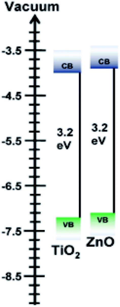 | ||
| Fig. 1 Schematic diagram for the energy levels of the conduction and valence band of TiO2 and ZnO Taken from ref. 5–7. | ||
In spite of the competitive efficiency of the organic–inorganic hybrid perovskite solar cells, the device hardly maintain integrity and functionality when exposed to the surroundings. Cesium (Cs) has been attempted to take the place of CH3NH3 (MA) to form all-inorganic halide perovskites CsPbX3 (X = Cl, Br, I) to realize relatively long stability. Perovskites CsPbX3 have found widespread applications in photo-electrics devices,17,18 due to the meritorious attributes like strong air/thermal stability, high light absorption coefficients, and phenomenal charge transporting with a reasonably long exciton diffusion length. Moreover, low temperature/cost ease solution processability allows for roll-to-roll manufacturing with flexible substrates.19 However, some issues still exist. A wide bandgap of 2.3 eV of CsPbBr3 limits its absorption, thus the best performance only with 10.6%. Despite an ideal bandgap of 1.73 eV, α-CsPbI3 (cubic phase) is merely stable at high temperature (>300 °C) and would become undesirable δ-CsPbI3 (non-perovskite phase) under ambient conditions.20 It would be hard to fabricate α-CsPbI3 based solar cells under the routine conditions. CsPbI2Br with a band gap of 1.91 eV, through partially substituting iodide (I) with bromide (Br)21,22 to tune the tolerance factor of perovskite structure, acts as a light absorber to improve overall device performance. In this work, a comparative study has been systematically conducted to investigate and evaluate the performance of ZnO, TiO2 and TiO2/ZnO as an electrode in perovskite CsPbI2Br solar cells.
Experimental section
Zinc acetate dihydrate (Zn(O2CCH3)2, 99.0%) served as a precursor to synthesize ZnO nanowires. 0.5 g of the precursor was placed in an alumina crucible, covered by an alumina lid, and then placed in a furnace. The crucible was heated to 300 °C and held for a period of 1–12 hours, producing ZnO nanowires with different qualities in a powdery form.23 By following different mass ratios, as-obtained ZnO and as-purchased TiO2 (99.99%) powder were thoroughly mixed up and put into dimethyl formamide (DMF) to make into solutions for developing films later on.The perovskite precursor solution was prepared by dissolving as-purchased CsBr (≥99.5%) and PbI2 (≥99.99%) at a 1![[thin space (1/6-em)]](https://www.rsc.org/images/entities/char_2009.gif) :1 molar ratio into a mixture of solvents with dimethyl sulfoxide (DMSO)/DMF ratio at 2:3 (improving the crystallization, exhibiting the least number of defects and forming the final pin-hole free films24) to make a solution with a concentration of ∼0.33 mol L−1. The solution was kept stirring overnight in an N2-filled glove box. For further characterization, the solution was dried at 100 °C for 10 min under nitrogen (N2) to evaporate the solvent.25
:1 molar ratio into a mixture of solvents with dimethyl sulfoxide (DMSO)/DMF ratio at 2:3 (improving the crystallization, exhibiting the least number of defects and forming the final pin-hole free films24) to make a solution with a concentration of ∼0.33 mol L−1. The solution was kept stirring overnight in an N2-filled glove box. For further characterization, the solution was dried at 100 °C for 10 min under nitrogen (N2) to evaporate the solvent.25
ITO glasses were cleaned by washing/rinsing with detergent and DI water. They were further cleaned by sonicating in acetone, and isopropanol for 10 min sequentially. After being thoroughly cleaned, the ITO glasses were dried in an oven with 100 °C. Before constructing solar cells, the ITO glass was treated with oxygen plasma for 2 min. The TiO2/ZnO solution with various ratios was spin-coated onto the treated ITO with a speed of 3000 rpm for 20 seconds as electron transporting layers. The as-prepared ITO/TiO2/ZnO substrates were placed into an N2-filled glovebox. The perovskite active layers were deposited onto the ITO/TiO2/ZnO substrates by spin-coating 30 seconds with speeds of 2000 rpm and 5000 rpm, respectively. Annealing with temperature of 100 °C was conducted for 10 minutes to obtain a CsPbI2Br film. Another batch of pre-cleaned ITO glasses was dip-coated with a carbon solution as the hole transporting layers. The solar cells were constructed by sandwiching perovskite covered ITO/TiO2/ZnO substrates and carbon blanketed ITO glasses.
Morphology was examined by scanning electron microcopy (JEOL JSM-IT800 FE-SEM). UV-vis optical absorption spectra were recorded in an absorbance mode on a Varian Cary Bio 50 UV-visible spectrophotometer. X-ray diffraction patterns were collected on a Rigaku Ultima IV diffractometer in a grazing incident mode with an incident angle of 0.5°. Cu K-alpha line (λ = 154.059 pm) was utilized as a light source. The current density–voltage characteristic curves both in the dark and under AM1.5 illumination (100 mW cm−2) were recorded by a Keithley 2400 source meter, in which current was continuously measured as a function of voltage with a step of 0.02 V. The power conversion efficiency of the devices were measured from an area of 1 × 1 cm2 under a small-area class-B solar simulator (PV Measurements, Inc.).
Results and discussions
The X-ray diffraction profile of the intrinsic light absorber CsPbI2Br was collected in a speed mode as shown in Fig. 2a. A single α black phase was detected, reflected by two strong diffraction peaks located at 14.9° and 30.0°, corresponding to the α phase of Cs1−xFAxPbI2Br.20,26 The ultraviolet-visible absorption spectroscopy, as presented in Fig. 2b, further confirmed that the perovskite film of CsPbI2Br was formed, identified by a strong absorbing peak at about 627 nm wavelength corresponding to an optical bandgap of 1.91 eV. Both XRD profile and UV-vis absorption results are consistent with the previous reports.27,28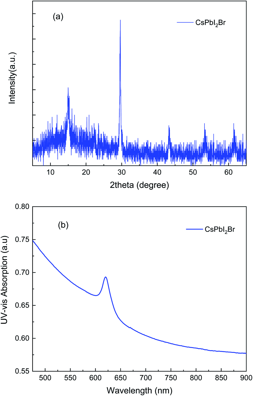 | ||
| Fig. 2 (a) XRD profile and (b) UV-vis absorption spectrum for CsPbI2Br. | ||
Scanning electron microscopy images in Fig. 3 disclose the morphology of various electron transporting films. Fig. 3a reveals that ZnO nanowires were randomly matted on the ITO glass. The nanowires with high quality and high purity were distributed forming a net-like film with up to a few micro-meters in length, about 40–60 nanometers in diameter. As purchased TiO2 nanoparticles were uniformly deposited and randomly connected on the substrate, as scrutinized in Fig. 3b, without any particular eye-striking feature. Fig. 3c and d suggest that the film with a TiO2/ZnO ratio at 99:1 shared the morphology similar to that of the one with a ratio of 97:3, so does the SEM of the film with 95:5 (not shown). Few random ZnO nanowires were decorated here or there on the very top surface. Network of ZnO nanowires was embedded in the film, which was revealed by the top topography as indicated by arrows. Due to the large amount in the solution, the film feature of TiO2 dominates on the surface area.
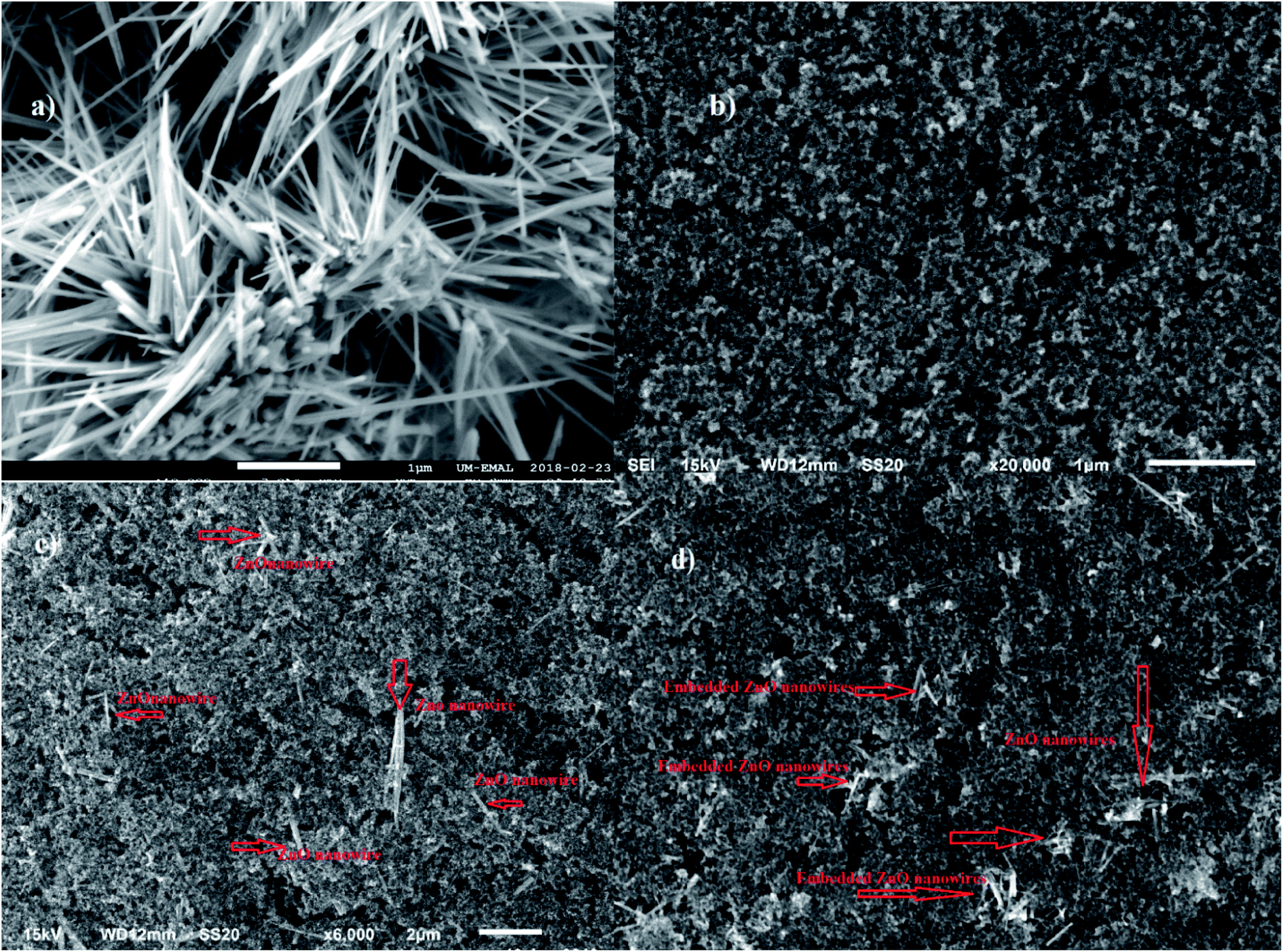 | ||
| Fig. 3 (a) Pure ZnO nanowires film (b) pure TiO2 film (c) film of TiO2/ZnO ratio at 99:1 (d) film of TiO2/ZnO ratio at 97:3. | ||
X-ray diffraction patterns in Fig. 4 corroborate that chemical composition and crystal structures of the mixtures. Fig. 4a indicates that the crystal structure of as-purchased TiO2 is anatase, which can be identified by diffraction peaks at 2θ values of 25°, 38.1°, 48.2°, 53.9° and 55.1°, corresponding to the reflection planes of (101), (004), (200) and (105), respectively.29 The XRD profile is in agreement with the standard XRD pattern (JCPDS files no. 21-1272). Fig. 4e portrays that the crystal structure of as-produced ZnO nanowires is a single hexagonal phase of wurtzite. ZnO nanowires, from hundred nanometers to micrometers in length, possess a space group of P63mc (JCPDS card no. 36-1451) with high crystallinity. The characteristic peaks are at 31.95°, 34.6°, 36.4°, 47.7°, 56.75°, 63.0° and 68.1°, which are ascribed to the crystal planes of (100), (002), (101), (102), (110), (103), and (112), respectively. Compared with the standard diffraction patterns of ZnO, the discrepancy in the relative weak peak intensities is attributed to the fact that nanowires have preferred growth orientations. Moreover, the relative peak intensity of (100) to (002) between 31.95° and 34.6° substantiates that ZnO nanowires synthesized by various methods exhibit different preferred growth orientations. Fig. 4b–d depict XRD profiles of the mixtures, clearly illustrating that with increase in amount of the mixtures, the characteristic peaks of the ZnO, (101) at 36.4° and (103) at 63.0° become more apparent, although the peak of (101) at 36.4° of ZnO is lumped together with that of (004) at 28.1° of TiO2.
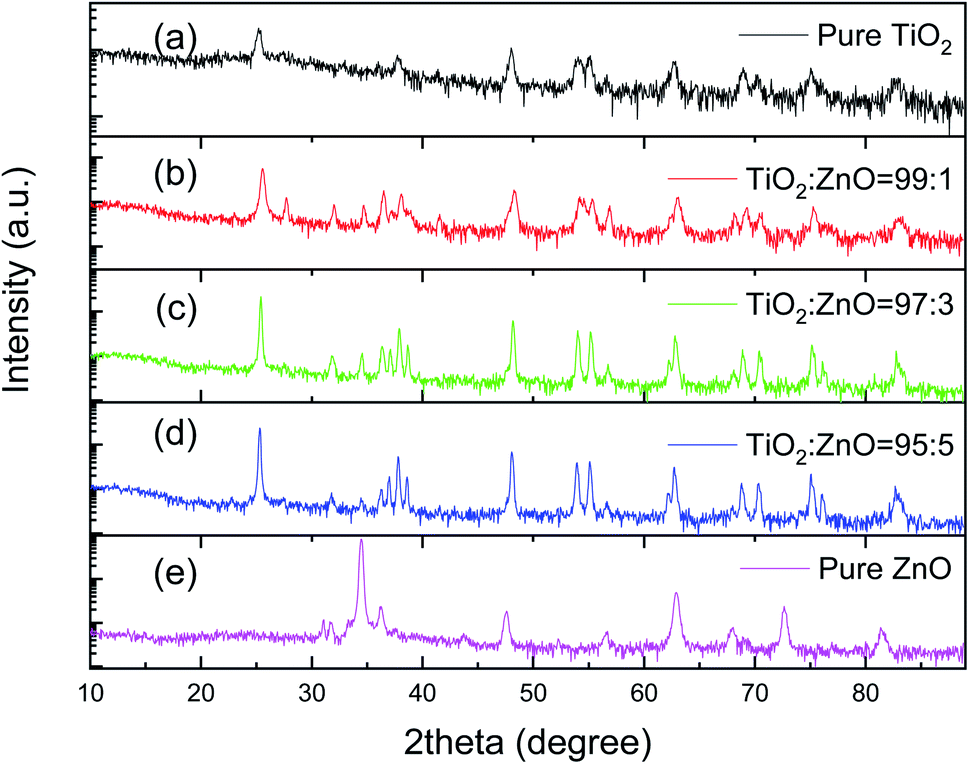 | ||
| Fig. 4 XRD profiles for all electron transporting layers, (a) pure TiO2; (b)TiO2:ZnO = 99:1; (c) TiO2:ZnO = 97:3; (d) TiO2:ZnO = 95:5; and (e) pure ZnO nanowires. | ||
Photovoltaic effects of all constructed solar cells were evaluated by the photo current–voltage curves under 1 sun illumination (∼100 mW cm−2) as depicted in Fig. 5. Generally speaking, the curves of solar cells with pure TiO2 and a ratio of 99:1 (in black and red, respectively) share the similar trend shape. While solar cells with pure ZnO and a ratio of 95:5 (in pink and blue) possess an I–V bending feature alike as portrayed in Fig. 5. Only the curve of the cell with a ratio of 97:3 stands alone (in green). Apparently, different electron transporting layers dramatically impact the performance of solar cells. For comparison sake, the important parameters for solar cells such as short circuit current density Jsc, open circuit voltage Voc, fill factor FF, and the calculated power conversion efficiency (PCE), were summarized in Table 1. For the pure TiO2/ZnO solar cells, the PCE reaches 4.95% and 3.95%, respectively. The TiO2 based solar cell slightly outperforms the ZnO-based counterpart. With varying the doping amount of ZnO from a ratio of 99:1 to 97:3, the PCE increases from 7.44% to 10.53%. However, the PCE drops to 7.11%, instead of keeping on increasing above 10.53% when further increasing the doping amount of ZnO at a ratio of 95:5.
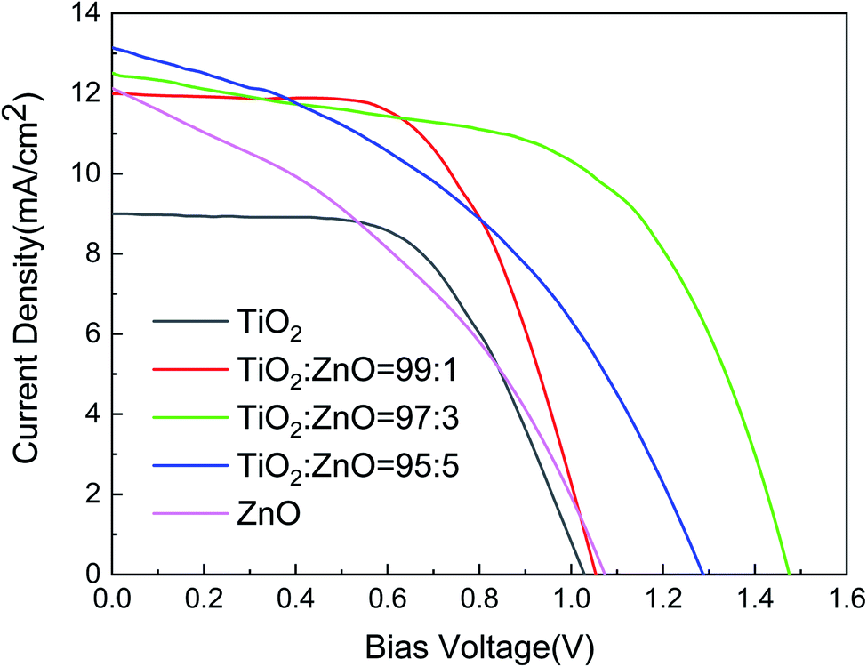 | ||
| Fig. 5 The current–voltage characterization of constructed solar cells with various ETL at different ratios of TiO2/ZnO. | ||
| Devices | Jsc (mA cm−2) | Voc (V) | FF | PCE% |
|---|---|---|---|---|
| TiO2 | 9.04 | 1.03 | 0.532 | 4.95 |
| TiO2:ZnO = 99:1 |
11.97 | 1.05 | 0.592 | 7.44 |
| TiO2:ZnO = 97:3 |
12.51 | 1.47 | 0.573 | 10.53 |
| TiO2:ZnO = 95:5 |
13.16 | 1.29 | 0.419 | 7.11 |
| ZnO | 12.18 | 1.07 | 0.303 | 3.95 |
TiO2 has a track record as an efficient ETL in perovskite solar cells because of its favorable energy level, easy fabrication and long electron lifetime.30,31 The effective mass of conduction band electrons in TiO2 is about 5–10 me as compared with 0.3 me of ZnO, implying the available density of states is almost 2 orders of magnitude higher in TiO2 than in ZnO, ensuring the faster and more efficient electron injection.32 On the other hand, the low electron mobility and relatively high density of electric trap states below the conduction band of TiO2 could thwart its performance, with the PCE of 4.95% in this study. As verified by the SEM images, ZnO nanowires have a much better crystalline quality, which facilitate electron diffusion by providing a direct pathway for electron transport from the point of electron injection to the metal wire because electrons would not suffer any grain boundary scattering. Photocurrent response time in nanowires is about 2 orders of magnitude faster (∼30 μs), indicating that electron transport in ZnO nanowires could be improved. TiO2 consists of small, randomly connected nanoparticles with a large number of grain boundaries, which act as traps/energy barriers slowing electron transport. The vast difference in the morphology of the films results in varying electron mobility. The electron mobility in ETL must be as fast as possible to efficiently extract the injected charges in order to minimize interfacial charge recombination losses. In theory, the ZnO based solar cell is expected to be better than the TiO2 based one. However, the ETL film of relatively more compact well-connected TiO2 nanoparticles provides more efficient pathways for electron extraction, compared with the layer of loosely netted ZnO nanowires rife with voids, which limits the microscopic electron transport and overshadows individual nanowire's faster electron transporting. It is no surprise that the ZnO based device performed poorly with a lower PCE of 3.95% in spite of better electron mobility.
With increase in the ZnO nanowire concentration from 99:1, 97:3 to 95:5, the PCE of the individual cells is 7.44%, 10.53% and 7.11%, respectively. The ZnO nanowires embedded TiO2 hybrid film significantly boosted the photovoltaic performance. When two semiconductors with slightly different conduction band edges and energy positions are adopted as an electron transporting layer, an allowed fast electron transfer process paves the way for better charge separation.33 The TiO2 permits the formation of an energy barrier at the ZnO, because TiO2 conduction band edge is somewhat more negative than that of ZnO. This energy barrier reduces the back electron transfer from conduction band of ZnO, thus decreasing the recombination rate and improving the cell performance. Moreover, as revealed in the SEM, the nanowires ZnO were developed into a matted film with voids. After mixing with nanoparticles TiO2, those voids could be filled up to form relatively more compact films. A more compact electron transporting layer could result in a low series resistance, a high recombination resistance, and a low charge transfer resistance, which greatly impact the photocurrent, evidenced by better Jsc of cells with hybrid films at 11.97 mA cm−2, 12.51 mA cm−2 and 13.16 mA cm−2, as listed in Table 1. Furthermore, the electron diffusion coefficient of ZnO nanowires is several hundred times higher than that of TiO2 nanoparticles.34 Due to the high crystal quality and collateral dimension, the introduction of ZnO nanowires reduces the number of grain boundaries and provides straight pathways for generated electrons to effortlessly pass through, instead of zigzagging through nanoparticles with numerous barriers leading to high possibility of recombination. Additionally, ZnO nanowires with lengths in the range of hundreds of nanometers to micrometers can serve as light scattering centers to enhance the light harvest efficiency. As a result, the better performance of solar cells with hybrid films can be attributed to the synergetic effect of both TiO2/ZnO constituent properties as electron transporting layers.
The PCE of the device with a hybrid film at a ratio of 97:3 reaches 10.53%, outperforming the one with 7.11% at a ratio of 95:5, suggesting that the higher concentration of ZnO nanowires does not ensure the better photovoltaic performance. A larger amount of ZnO nanowires in ETL could shift the conduction band of electrode, which impedes the charge separation and efficient transporting to the semiconductor electrode, thus being detrimental in photovoltaic performance.35 Therefore, it could be reasonably argued that an appropriate amount of ZnO nanowires embedded in TiO2 films could optimize the ETL property by improving charge separation, charge transporting and light harvesting, consequentially, elevating the overall photovoltaic performance.
Different possible factors can affect the ideality values (the curve shape) such as: series resistance, shunt resistance, temperature, carriers' mobility, tunneling, generation-recombination, interface impurity, interfacial oxide layer and so on. Some localized defect states of TiO2/ZnO may lie in semiconductors' forbidden gap. The semiconductor localized states can act as carrier trapping centers. Carriers from electrodes trapped in these centers and these localized states become charged. Subsequently, a space charge region would be built up, which has a strong effect on the J–V characteristics of a device, especially at higher bias levels because the trapped carriers contribute to the conduction paths. The unique J–V characteristics of the cell with a ratio of 97:3 results from the presence of the built-up charged region, which minimizes the energy loss, leading to the highest Voc of 1.47 V. By ruling out the other factors, the non-ideality in a solar cell is largely associated with the shunt resistance (Rsh) and the series resistance (Rs) as depicted in Fig. 6a. The series resistance and shunt resistance can be calculated by −dV/dJ based on the diode equation for each cell.36 Roughly speaking, solar cells with pure TiO2 and a ratio of 99:1 (in black and red, respectively) share the comparable Rsh and Rs, leading to the curve shape alike. While Rsh and Rs in solar cells based on pure ZnO and a mixture with a ratio of 95:5 are close enough to share the similar −dV/dJ at V approaching to 0 and V > Voc as illuminated in Fig. 6b.
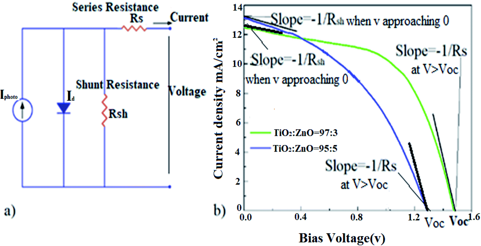 | ||
| Fig. 6 (a) Diagrammatic sketch of the equivalent circuit of a solar cell (b) estimated R-shunt and R-series. | ||
Due to the increased effective tolerance factor, CsPbI2Br has demonstrated enhanced phase stability when exposed to moisture in ambient conditions, compared with other all inorganic Cs-based perovskites.37 Since being first developed, the PCE of CsPbI2Br based solar cells has been reported to achieve 16.37% within 2 years,38 which holds great potential for breakthroughs in the solar energy field. Certainly, a substantial amount of research to ameliorate all components of n-i-p solar cells is still needed to bridge the gap between today's benchmark conversion efficiency and the predicted 32% by the Shockley-Queisser limit of a single junction cell. At present, no material/configuration of devices has been identified as the best option to optimize the overall performance of perovskite solar cells. The obtained insights in this work could provide some rationales on design of better performing perovskite solar devices, a step forward in realization of practical applications, which could pave the way for further improvement, and accelerate more breakthroughs in perovskite solar cells for eventual commercialization.
Conclusions
The relatively more stable all-inorganic CsPbI2Br has been attempted as a light absorber, along with various electron transporting films to construct solar cells. The comparative study was conducted to look into the photovoltaic performance for all solar devices. It turns out that solar cells with ZnO nanowires embedded TiO2 as an electrode outperformed those with pure TiO2 or pure ZnO. The enhanced performance is attributed to the synergetic effect of both TiO2/ZnO constituent properties. TiO2 nanoparticles with the longer electron life time/higher density of states, in conjunction with ZnO nanowires with the better electron mobility/light harvesting, formed a compact electron selective layer with lower charge transfer resistance, leading to the better power conversion efficiency. In particular, an appropriate amount of ZnO nanowires embedded in TiO2 films could optimize the property electron transport layer by improving charge separation, charge transporting and light harvesting, as a result, the highest power conversion efficiency of 10.53% among them can be achieved.Conflicts of interest
Authors declare there is no conflict of interest.Acknowledgements
This work was supported by National Science Foundation (NSF) (Grant No. 1700339).References
- A. Kojima, K. Teshima, Y. Shirai and T. Miyasaka, Organometal Halide Perovskites as Visible-Light Sensitizers for photovoltaic Cells, J. Am. Chem. Soc., 2009, 131, 6050 CrossRef CAS PubMed
.
- H. S. Jung and N. G. Park, Perovskite Solar Cells: From Materials to Devices, Small, 2015, 11, 10 CrossRef CAS PubMed
- NREL efficiency chart, https://www.nrel.gov/pv/assets/images/efficiency-chart.png.
- K. Domanski, J. Correa-Baena, N. Mine, M. Nazeeruddin, A. Abate, M. Saliba, W. Tress, A. Hagfeldt and M. Grätzel, Not All That Glitters Is Gold: Metal-Migration-Induced Degradation in Perovskite Solar Cells, ACS Nano, 2016, 10, 6306 CrossRef CAS PubMed
- J. Y. Guan, J. Ni, X. J. Zhou, Y. Liu, J. Y. Yin, J. L. Wang, D. Wang, Y. F. Zhang, J. Li, H. K. Cai and J. J. Zhang, High-Performance Electron Transport Layer via Ultrasonic Spray Deposition for Commercialized Perovskite Solar Cells, ACS Appl. Energy Mater., 2020, 3(12), 11570–11580 CrossRef CAS
- E. Sundin, R. Ringström, F. Johansson, B. Küçüköz, A. Ekebergh, V. Gray, B. Albinsson, J. Mårtensson and M. Abrahamsson, Singlet Fission and Electron Injection from the Triplet Excited State in Diphenylisobenzofuran–Semiconductor Assemblies: Effects of Solvent Polarity and Driving Force, J. Phys. Chem. C, 2020, 124(38), 20794–20805, DOI:10.1021/acs.jpcc.0c06626
- J. A. Smith, O. S. Game, J. E. Bishop, E. L. K. Spooner, R. C. Kilbride, C. Greenland, R. Jayaprakash, T. I. Alanazi, E. J. Cassella, A. Tejada, G. Chistiakova, M. l. Wong-Stringer, T. J. Routledge, A. J. Parnell, D. B. Hammond and D. G. Lidzey, Rapid Scalable Processing of Tin Oxide Transport Layers for Perovskite Solar Cells, ACS Appl. Energy Mater., 2020, 3(6), 5552–5562, DOI:10.1021/acsaem.0c00525
- R. Jose, V. Thavasi and S. Ramakrishna, Metal Oxides for Dye-Sensitized Solar Cells, J. Am. Ceram. Soc., 2009, 92, 289 CrossRef CAS
- D. Q. Bi, G. Boschloo, S. Schwarzmullker, L. Yang, E. M. Johansson and A. Hagfeldt, Efficient and stable CH3NH3PbI3-sensitized ZnO nanorode array solid state solar cells, Nanoscale, 2012, 5, 11686 RSC
- D. Y. Son, J.-H. Im, H. S. Kim and N.-G. Park, 11% Efficient Perovskite Solar Cell Based on ZnO Nanorods: An Effective Charge Collection System, J. Phys. Chem. C, 2014, 118, 16567–16573 CrossRef CAS
- J. J. Shi, X. Xu, D. M. Li and Q. B. Meng, Interfaces in Perovskite Solar Cells, Small, 2015, 11(No. 21), 2472–2486 CrossRef CAS PubMed
- P. Tiwana, P. Docampo, M. B. Johnston, H. J. Snaith and L. M. Herz, Electron Mobility and Injection Dynamics in Mesoporous ZnO, SnO2, and TiO2 Films Used in Dye-Sensitized Solar Cells, ACS Nano, 2011, 5158–5166 CrossRef CAS
- Y. Q. Wang, Y. M. Sun and K. Li, Dye-sensitized solar cell based on oriented ZnO nanowire-covered TiO2 nanoparticle composite film electrodes, Mater. Lett., 2002, 63, 1102–1104 CrossRef
- Y. Bai, H. Yu, Z. Li, R. Amal, G. Q. Liu and L. Z. Wang, In Situ Growth of a ZnO nanowire network within a TiO2 nanoparticle film for enhanced dye-sensitized solar cell performance, Adv. Mater., 2012, 24, 5850–5856 CrossRef CAS PubMed
- W. P. Hu, S. F. Yang and S. H. Yang, Surface Modification of TiO2 for Perovskite Solar Cells, Trends Chem., 2020, 148–162 CrossRef CAS
- J. Luo, Y. X. Wang and Q. F. Zhang, Progress in perovskite solar cells based on ZnO nanostructures, J. Sol. Energy, 2018, 289–306 CrossRef
- Z. P. Hu, Z. Z. Liu, Y. Bian, D. J. Liu, X. S. Tang, W. Hu, Z. G. Zang, M. Zhou, L. D. Sun, J. X. Tang, Y. Q. Li, J. Du and Y. X. Leng, Robust Cesium Lead Halide Perovskite Microcubes for Frequency Upconversion Lasing, Adv. Opt. Mater., 2017, 5, 1700419, DOI:10.1002/adom.201700419
- J. Z. Song, J. H. Li, X. M. Li, L. M. Xu, Y. H. Dong and H. B. Zeng, Quantum Dot Light-Emitting Diodes Based on Inorganic Perovskite Cesium Lead Halides, Adv. Mater., 2015, 27, 7162–7167, DOI:10.1002/adma.201502567
- Y. Li, Z.-F. Shi, S. Li, L.-Z. Lei, H.-F. Ji, D. Wu, T.-T. Xu, Y.-T. Tian and X.-J. Li, High-performance perovskite photodetectors based on solution-processed all-inorganic CsPbBr3 thin films, J. Mater. Chem. C, 2017, 5, 8355–8360, 10.1039/c7tc02137b
- G. E. Eperon, G. M. Paterno, R. J. Sutton, A. Zampetti, A. A. Haghighirad, F. Cacialli and H. J. Snaith, Inorganic caesium lead iodide perovskite solar cells, J. Mater. Chem. A, 2015, 3, 19688–19695 RSC
- L. Yan, Q. Xue, M. Liu, Z. Zhu, J. Tian, Z. Li, Z. Chen, Z. Chen, H. Yan, H.-L. Yip and Y. Cao, Interface Engineering for All-Inorganic CsPbI2Br Perovskite Solar Cells with Efficiency over 14%, Adv. Mater., 2018, 30, 1802509 CrossRef PubMed
- Y. Guo, X. Yin, J. Liu and W. Que, Highly efficient CsPbIBr2 perovskite solar cells with efficiency over 9.8% fabricated using a preheating-assisted spin-coating method, J. Mater. Chem. A, 2019, 7, 1900 RSC
- C.-C. Lin and Y.-Y. Li, Synthesis of ZnO nanowires by thermal decomposition of zinc acetate dihydrate, Mater. Chem. Phys., 2009, 113, 334–337 CrossRef CAS
- S. Zhang, S. Wu, W. Chen, H. Zhu, Z. Xiong, Z. Yang, C. Chen, R. Chen, L. Han and W. Chen, Solvent engineering for efficient inverted perovskite solar cells based on inorganic CsPbI2Br light absorber, Mater. Today Energy, 2018, 8, 125 CrossRef
- Y. L. Z. F. Shi, S. Li, L. Z. Lei, H. F. Ji, D. Wu, T. T. Xu, Y. T. Tian and X. J. Li, High performance perovskite photodetectors based on solution-processed all-inorganic CsPbX3 thin films, J. Mater. Chem. C, 2017, 5, 8355–8360, 10.1039/C7TC02137B
- C. C. Stoumpos and M. G. Kantzidis, The renaissance of halide perovskites and their evolution as emerging semiconductors, Acc. Chem. Res., 2015, 48(10), 2791–2802 CrossRef CAS
- K. Ubaid, Z. N. Yu, A. K. Abbas, Z. Almas and U. Naeem, High performance CsPbI2Br perovskite solar cells with Zinc and Manganese doping, Nanoscale Res. Lett., 2019, 14, 116 CrossRef
- J. G. Zhang, Z. W. Jin, L. Liang, H. R. Wang, D. L. Bai, H. Bian, K. Wang, Q. Wang, N. Y. Yuan, J. N. Ding and S. Z. Liu, Iodine-Optimized Interface for Inorganic CsPbI2Br Perovskite Solar Cell to Attain High Stabilized Efficiency Exceeding 14%, Adv. Sci., 2018, 5, 1801123 CrossRef
- A. J. Haider, R. H. Al-Anbari, G. R. Kadhim and C. T. Salame, Exploring potential environmental applications of TiO2 nanoparticles, Energy Procedia, 2017, 119, 332–345 CrossRef CAS
- M. Liu, M. B. Johnston and H. J. Snaith, Efficient planar
heterojunction perovskite solar cells by vapor deposition, Nature, 2013, 501, 395 CrossRef CAS PubMed
- J. Burschka, N. Pellet, S.-J. Moon, R. Humphry-Baker, P. Gao, M. K. Nazeeruddin and M. Grätzel, Sequential deposition as a route to high-performance perovskite-sensitized solar cells, Nature, 2013, 499, 316 CrossRef CAS PubMed
- N. A. Anderson, X. Ai and T. Q. Lian, Electron injection dynamics for Ru Polypyridyl complexes to ZnO nanocrystalline think films, J. Phys. Chem. B, 2003, 107, 14414–14421 CrossRef CAS
- C. K. Xu, J. M. Wu, U. V. Desai and D. Gao, High efficiency solid state dye-sensitized solar celled based on TiO2 coated ZnO nanowire arrays, Nano Lett., 2012, 12, 2420–2424 CrossRef CAS PubMed
- M. Law, L. E. Greene, J. C. Johnson, R. Saykally and P. Yang, Nanowire dye-sensitized solar, Nat. Mater., 2005, 4, 455 CrossRef CAS PubMed
- S. Pang, T. F. Xie, Y. Zhang, X. Wei, M. Yang, D. J. Wang and Z. L. Du, Research on the Effect of Different Sizes of ZnO Nanorods on the Efficiency of TiO2-Based Dye-Sensitized Solar Cells, J. Phys. Chem. C, 2007, 111, 18417 CrossRef CAS
- W. J. Ke, G. J. Fang, J. Wang, P. L. Qin, H. Tao, H. W. Lei, Q. Liu, X. Dai and X. Z. Zhao, Perovskite Solar Cell with an Efficient TiO2 Compact Film, ACS Appl. Mater. Interfaces, 2014, 6, 15959–15965 CrossRef CAS PubMed
- Q. S. Zeng, X. Y. Zhang, C. M. Liu, T. L. Feng, Z. L. Chen, W. Zhang, W. T. Zheng, H. Zhang and B. Yang, Inorganic CsPbI2Br Perovskite solar cells: the progress and perspective, Advanced Science, Sol. RRL, 2019, 3, 1800239 CrossRef
- Y. Q. Zhang, C. C. Wu, D. Wang, Z. H. Zhang, X. Qi, N. Zhu, G. H. Liu, X. D. Li, H. Z. Hu, Z. J. Chen, L. X. Xiao and B. Qu, High Efficiency (16.37%) of Cesium Bromide—Passivated All-Inorganic CsPbI2Br Perovskite Solar Cells, Sol. RRL, 2019, 3, 1900254 CrossRef CAS
| This journal is © The Royal Society of Chemistry 2021 |