
 Open Access Article
 This Open Access Article is licensed under a Creative Commons Attribution-Non Commercial 3.0 Unported Licence
Abundant topological phases in hydrogenated group-IV binary alloy compounds†
Guanyi Gaoa,
Hairui Baoa,
Bao Zhaoab,
Hao Huana and
Zhongqin Yang *ac
*ac
aState Key Laboratory of Surface Physics and Key Laboratory of Computational Physical Sciences (MOE), Department of Physics, Fudan University, Shanghai 200433, China. E-mail: zyang@fudan.edu.cn
bSchool of Physics Science and Information Technology, Shandong Key Laboratory of Optical Communication Science and Technology, Liaocheng University, Liaocheng 252059, China
cCollaborative Innovation Center of Advanced Microstructures, Nanjing 210093, China
First published on 16th April 2021
Abstract
Based on the widely studied two-dimensional layered materials, new materials with unique properties can be acquired by stacking the layered materials with different styles. By using density-functional calculations and symmetry analysis, we here present a route to produce abundant topologically nontrivial electronic states in three-dimensional compounds made of stacked monolayer hydrogenated group-IV binary alloys. Triply degenerate point (TDP) semimetals and Dirac semimetals are found in the hydrogenated SnPb compounds with different stacking configurations. The TDP semimetal is characterized by two sets of near-Dirac TDPs, stemming from the inversion of the s (pz) and px,y bands from the Pb (and also Sn) atoms and protected by a C3v double point group symmetry. Type-I and type-II states, and one essential Dirac semimetal state, coexist in a hydrogenated SnPb compound. Hourglass surface states are also observed in this case. For the hydrogenated GeSn and GePb compounds, normal insulators and weak topological insulators (and also Dirac semimetals) are obtained, respectively. The topological nature of the states is identified by calculations of topological indexes as well as surface states. With these extremely rich topological phases, the studied compounds offer an ideal material platform for realizing topological semimetals and insulators in experiments.
1. Introduction
Some of the most important discoveries in condensed matter physics over the last few decades have been about topological states of matter. Topological materials1–4 feature an electronic band structure that exhibits a special band topology not determined by the Landau order parameter and the concept of symmetry breaking. The topologically protected electronic states are generally immune to environmental perturbations, making the topological materials promising for applications in low-dissipation and high-reliability microelectronic devices. Among the rich variety of topological materials, topological semimetals2,5–9 have sparked intense research interest. Topological semimetals with zero-dimensional band crossings are characterized by discrete band degenerate points in the bulk spectra, in which these discrete points connect with open strings formed by topologically protected surface states on the boundaries, called Fermi arc states.8 Very exotic physical properties and further potential applications2,9–11 can stem from the Fermi arc states. For example, the proximity-induced surface superconductivity found in the Dirac semimetal (DSM) Cd3As2 provides possibilities to manipulate superconducting quantum states,12,13 which may be a building block for topological quantum computations. The spin-momentum-locking property of the Fermi arcs14,15 is similar to the surface states of topological insulators, auspicious for current-induced spin polarization and realistic spintronic applications.Currently, plenty of theoretical studies have been performed to produce topological semimetals.2,5–9,16–20 However, very little preliminary experimental progress has been achieved to date, such as in Na3Bi,21 Cd3As2,22 and WC-type materials,23,24 leaving many important physical effects not ready for practical applications. Some shortcomings or difficulties in utilizing the unique properties include: (i) the semimetal materials are generally difficult to fabricate and integrate in experiments.5,25 (ii) The quasiparticle excitations around the discrete band degenerate points may be far away from the Fermi level (EF).24 Thus, the unique transport phenomena originating from the band degenerate points are difficult to observe. (iii) The band degenerate points may coexist with other unconcerned bands.26–28 To further advance this field, we should go beyond the existing materials and find new topological semimetals without these drawbacks.
Van der Waals (vdW) layered systems represent a large family of materials with many tunable properties.29–35 For instance, topological insulating states were previously found in the tetradymite-type Bi2Te3-class materials,34 and Weyl semimetal states were observed in transition metal chalcogenides.35 Currently, a new class of monolayer group-IV XPb (X = C, Si, Ge and Sn) alloys has been reported to be mechanically stable,36 and their hydrogenated compounds can be topological insulators with large energy gaps.37,38 Whether the topological properties of the hydrogenated XPb monolayers are similar to those of their three-dimensional (3D) crystals and the influences of vdW interactions on the electronic states remain to be explored. Particularly, two-dimensional (2D) Ge/Sn graphane-like alloys have been successfully synthesized via the topochemical deintercalation of CaGe2−2xSn2x in aqueous acidic conditions39 and are suitable for fabrication into microelectronic devices. Thus, it is highly meaningful to explore the electronic states and possible topological behaviors of these 3D crystals built with pieces of these interesting and applicable 2D group-IV alloys.
In this work, we theoretically predict the existence of rich topological semimetal and insulating phases in hydrogenated group-IV binary alloy compounds. The hydrogenated SnPb (SnPbH2) compounds can host the triply degenerate point (TDP) semimetal phase and the DSM phase, depending on the different stacking configurations. The TDP semimetal (TDPSM) is characterized by two sets of “near-Dirac” TDPs near the EF, originating from the inversion of the s (pz) and px,y bands of the Pb (and also Sn) atoms and protected by a C3v double point group symmetry. The band inversion mechanism is explored by tuning the vdW interlayer space, which provides a clear physical picture of the band evolution from monolayers to 3D topological semimetals. The DSM features hourglass surface states, with two clean type-I Dirac points located exactly at the EF, protected by a C6v double point group symmetry. Two type-II points and a single essential Dirac point are also found coexisting near the EF in the system. Normal insulators and weak topological insulators (and also DSMs) are achieved in the hydrogenated GeSn (GeSnH2) and GePb (GePbH2) systems, respectively. Our discoveries provide a new route to produce the interesting topological phases from 2D materials.
2. Models and methods
We now take SnPbH2 as an example to analyze its topological electronic properties. The geometries of the SnPbH2 monolayer are displayed in Fig. 1(a), in which the Sn and Pb atoms together form a buckled honeycomb structure with H atoms bonded to the Sn or Pb atoms on both sides of the plane in an alternating manner. The thermal and dynamical stability of the monolayer SnPbH2 is illustrated in Fig. S1 of part A in the ESI.† The studied 3D SnPbH2 crystals are built by stacking the pieces of the SnPbH2 monolayers. In total, ten typical types of stacking configurations are considered, as shown in Table 1 and Fig. S2 in part B of the ESI.† The AR′ and AR′′ stacking configurations, renamed to C1 and C2, respectively, are displayed in Fig. 1(b). The first Brillouin zone (BZ) and the associated projected (11![[2 with combining macron]](https://www.rsc.org/images/entities/char_0032_0304.gif) 0) plane of the above two configurations are shown in Fig. 1(c).
0) plane of the above two configurations are shown in Fig. 1(c).
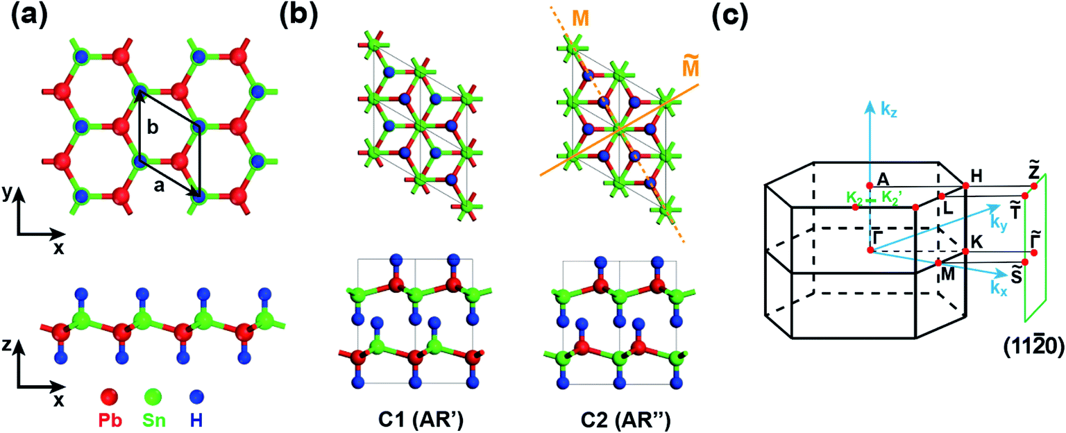 | ||
Fig. 1 (a) Top and side views of the monolayer SnPbH2. The black solid lines indicate the unit cell. (b) Top and side views of the 2 × 2 × 1 supercells of the two 3D SnPbH2 crystals with the C1 (AR′) and C2 (AR′′) configurations, respectively. The yellow solid line and yellow dashed line in the top view of the C2 configuration indicate a glide mirror plane ![[M with combining tilde]](https://www.rsc.org/images/entities/i_char_004d_0303.gif) and a mirror plane M in the structure, respectively. (c) The first BZ of the 3D SnPbH2 crystals with the C1 and C2 stacking configurations. Its projection onto the (110) plane is also shown. The green line K2–K2′ is on the kx–ky plane with the kz = 0.398 × 2π/c. and a mirror plane M in the structure, respectively. (c) The first BZ of the 3D SnPbH2 crystals with the C1 and C2 stacking configurations. Its projection onto the (110) plane is also shown. The green line K2–K2′ is on the kx–ky plane with the kz = 0.398 × 2π/c. | ||
| Symmetry | n | a (Å) | c/n (Å) | Δ (eV) | Band gap (meV) | ΔEexf (J m−2) | |
|---|---|---|---|---|---|---|---|
| AA | P3m1(156) | 1 | 4.846 | 4.821 | −6.284 | 0 | 0.214 |
| AA′ | P![[3 with combining macron]](https://www.rsc.org/images/entities/char_0033_0304.gif) m1(164) m1(164) |
2 | 4.843 | 4.830 | −6.275 | 0 | 0.207 |
| AR | P63mc(186) | 2 | 4.863 | 4.571 | −6.302 | 0 (DSM) | 0.227 |
| AR′ (C1) | P3m1(156) | 2 | 4.866 | 4.548 | −6.314 | 0 (TDPSM) | 0.236 |
| AR′′ (C2) | P63mc(186) | 2 | 4.872 | 4.477 | −6.324 | 0 (DSM) | 0.243 |
| AF | P![[6 with combining macron]](https://www.rsc.org/images/entities/char_0036_0304.gif) m2(187) m2(187) |
2 | 4.814 | 6.332 | −6.117 | 383.1 | 0.084 |
| AF′ | P63mc (186) | 2 | 4.810 | 6.448 | −6.116 | 364.6 | 0.083 |
| AX | P3m1(156) | 2 | 4.879 | 5.065 | −6.276 | 97.5 | 0.205 |
| AX′ | Pm1(164) |
2 | — | — | — | — | — |
| AX′′ | Pm1(164) |
2 | 4.889 | 5.117 | −6.270 | 66.5 | 0.200 |
The electronic structures of the hydrogenated group-IV binary alloy compounds are calculated within the framework of density-functional theory (DFT), as implemented in the Vienna ab initio simulation package (VASP).40,41 The Perdew–Burke–Ernzerhof generalized gradient approximation (GGA-PBE) is used to describe the exchange and correlation functional.42 The kinetic energy cutoff of the plane wave basis is set to be 500 eV. The convergence criterion for the total energy is set to 10−5 eV. The 15 × 15 × 15 and 15 × 15 × 7 Γ center Monkhorst–Pack grids are employed to perform the first BZ integral for the AA and the other nine configurations, respectively. All atoms in the unit cells are allowed to move until the Hellmann–Feynman force on each atom is smaller than 0.01 eV Å−1. The lattice constants of the unit cell are simultaneously relaxed. The interlayer vdW interactions are taken into consideration by applying the optB86b-vdW correlation functional.43,44 The topological properties are investigated by constructing the maximal localized Wannier functions using the WANNIER90 (ref. 45) package combined with the WANNIERTOOLS code.46 To check the possible underestimation of band gaps in the PBE functional, hybrid-functional methods based on the HSE06 scheme47 are adopted for the C1 and C2 SnPbH2 crystals. The band structures obtained with the HSE06 functional are given in Fig. S3 and analyzed in the ESI.†
3. Results and discussion
The symmetries, optimized lattice constants, and average total energy per layer obtained for the 3D SnPbH2 crystals with different stacking configurations are given in Table 1. Except for the AX′ configuration, all the other configurations considered form stable vdW layered crystals. The in-plane lattice constants (a) of the nine stable crystals are very close to that (4.89 Å) of the monolayer SnPbH2.38 The average interlayer spaces between the two adjacent layers are, however, very diverse due to the different stacking configurations. As displayed in Table 1, the configurations of C1 and C2 have the two smallest lattice constants c per layer (c/n), corresponding to stronger interlayer interactions of these two stacking configurations. Thus, these two stacking configurations reasonably have the lowest total energies compared to those of the other seven stacking configurations. The exfoliation energies of the stable configurations are calculated through ΔEexf = (Eiso − Ebulk/n)/A, where Eiso, Ebulk, n, and A represent the energy of the unit cell of an isolated monolayer SnPbH2, the energy of the unit cell of the 3D SnPbH2 crystal, the number of the SnPbH2 layers in the unit cell, and the in-plane area of the 3D SnPbH2 unit cell, respectively. The calculated exfoliation energies per layer48 of the stable configurations range from 0.083 J m−2 to 0.243 J m−2, lower than that of graphene exfoliated from graphite (0.37 J m−2).49 Thus, the vdW interactions between the two neighboring layers in the crystals are weak due to the H atoms saturating the pz dangling bonds of the Sn and Pb atoms. In the following, we focus on the two most stable stacking configurations of C1 and C2 for the 3D vdW SnPbH2 crystals. The dynamical stability of the above two configurations is confirmed by the calculations of the phonon spectra. As illustrated in Fig. S4 of the ESI,† no soft phonon mode appears for the two structures.We now study the topological electronic structures of the C1 SnPbH2, which owns a space group P3m1. Its orbital-resolved band structure is displayed in Fig. 2(a), where the spin–orbit coupling (SOC) is not considered. Obviously, the system shows gapless metallic behaviors around the EF, with the bands contributed by the Pb (and also Sn) s and p orbitals. Along the Γ–A line, the point group symmetry is C3v, with one 2D (Λ3) and two one-dimensional (1D) (Λ1, Λ2) irreducible representations (IRs). Without SOC, the s (also pz) orbitals and the px,y orbitals belong to the Λ1 and Λ3 IRs, respectively (Fig. 2(b)). Once the SOC is included, the crystal symmetry changes from the C3v group symmetry to the C3v double group symmetry. The C3v double group contains one 2D (Λ4) IR and two 1D (Λ5, Λ6) IRs. When the SOC is turned on, the Λ1 band changes to the Λ4 band and downshifts in energy, while the Λ3 splits into the (Λ4 + Λ5 + Λ6) bands, leading to two pairs of TDPs appearing near the EF and at 105 meV above the EF along the Γ–A line (marked by two red circles in Fig. 2(d)). The bands around the TDPs near the EF are magnified in Fig. 2(e). The double degeneracy of the Λ4 band comes from the existence of the σv mirror symmetry contained in the C3v point group of the C1 configuration. If the σv mirror symmetry is broken, each TDP will split into two Weyl points with opposite chiralities. The dispersion around TDP1 in the kx–ky plane is highlighted in Fig. 2(f), which shows how the bands near the TDP1 disperse away from the Γ–A line. As displayed in Fig. 2(e), the energy splitting of the Λ5 and Λ6 bands is about 3 meV. With such small splitting, TDP1 and TDP2 can be regarded together as a near-Dirac semimetal.50 The obtained results provide a promising venue for observing the DSMs and studying the related exotic properties.
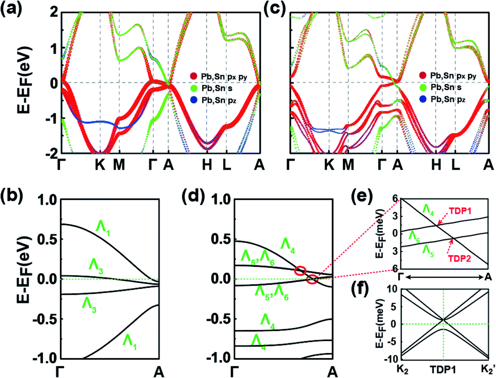 | ||
| Fig. 2 (a) Band structure of the C1 SnPbH2 crystal without SOC. The sizes of the dots are proportional to the orbital contributions. (b) Amplified band structure of (a) along the high-symmetry line Γ–A. (c) and (d) are the same as (a) and (b), respectively, except with the SOC considered. Two pairs of TDPs in (d) are marked by red circles. (e) The amplified band structure of the TDPs closer to EF in (d). The two TDPs in (e) are labeled TDP1 and TDP2, respectively. (f) Band structure in the kx–ky plane surrounding the TDP1. The K2 and K2′ points are displayed in Fig. 1(c). | ||
To deeply comprehend the origination of TDP1 and TDP2, we analyze the evolution of energy bands near EF with varying lattice constant in the absence of SOC, as illustrated in Fig. 3. When the interlayer space is large enough (c = 20 Å), the interaction between the two adjacent layers is negligible, leading to the weak band dispersion along the kz axis (between Γ and A points) (Fig. 3(a)). At this stage, the L1 and L2 bands (primarily composed of the px,y orbitals), as well as the L3 and L4 bands (primarily composed of the s and pz orbitals), are approximately degenerate. As the interlayer space decreases, the band dispersion increases gradually, especially for the L3 and L4 bands, due to the s and pz orbitals being sensitive to interlayer interactions (Fig. 3(b) and (c)). When the interlayer space reaches the equilibrium space c = 9.096 Å, the L3 band successively crosses the L2 and L1 bands along the Γ–A line, leading to the band inversion occurring at both the Γ and A points. Eventually, inclusion of the SOC interaction leads to the Λ4 band intersecting with the Λ5 and Λ6 bands along the Γ–A line. Such intersection between singly and doubly degenerate bands results in the TDPs for the C1 SnPbH2 crystal. Thus, the TDP1 and TDP2 appear due to band inversion of the s, pz and px,y orbitals and protection by the C3v double group symmetry.
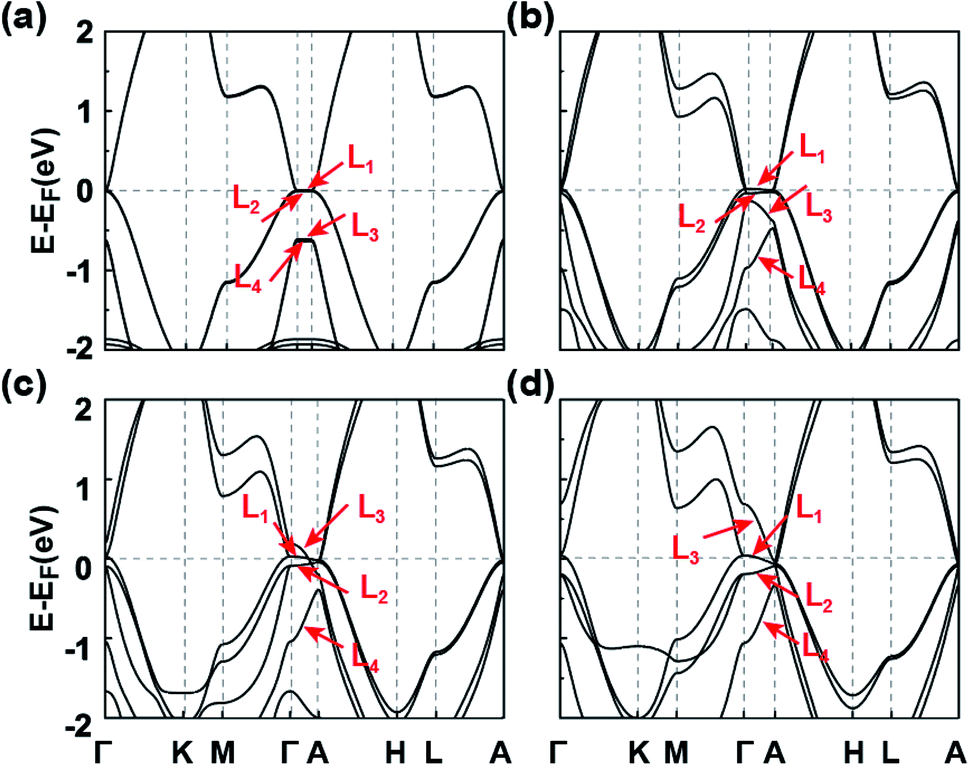 | ||
| Fig. 3 Band structures of the C1 SnPbH2 crystal with the lattice constants c of (a) 20 Å, (b) 11 Å, (c) 10 Å, and (d) 9.096 Å, respectively. The distance between the two layers in the unit cell varies accordingly. The SOC is not considered. | ||
The topological behaviors of the C1 SnPbH2 crystal are discussed based on the calculated surface states and the Fermi arcs (Fig. 4). Fig. 4(a) and (b) show the surface bands and the Fermi surface contour on the (110) plane, respectively. On this plane, the Dirac cone state has its branches merging into the bulk states, and an arc-like Fermi surface is achieved. As shown in Fig. 4(b), two Fermi arcs touch each other at the plane projection of the two bulk Dirac points. The Fermi surface contours on the (110) plane with tuned EF are emphasized in Fig. 4(c), clearly illustrating the evolution of the Fermi arc states. These Fermi arcs are also protected by bulk Z2 invariants, which are well defined in both kz = 0 (Z2 = 1) and kz = π (Z2 = 0) planes. Thus, a Kramers pair of surface states must exist on the kz = 0 path for the side surfaces, ensuring the presence of a pair of surface Fermi arcs.
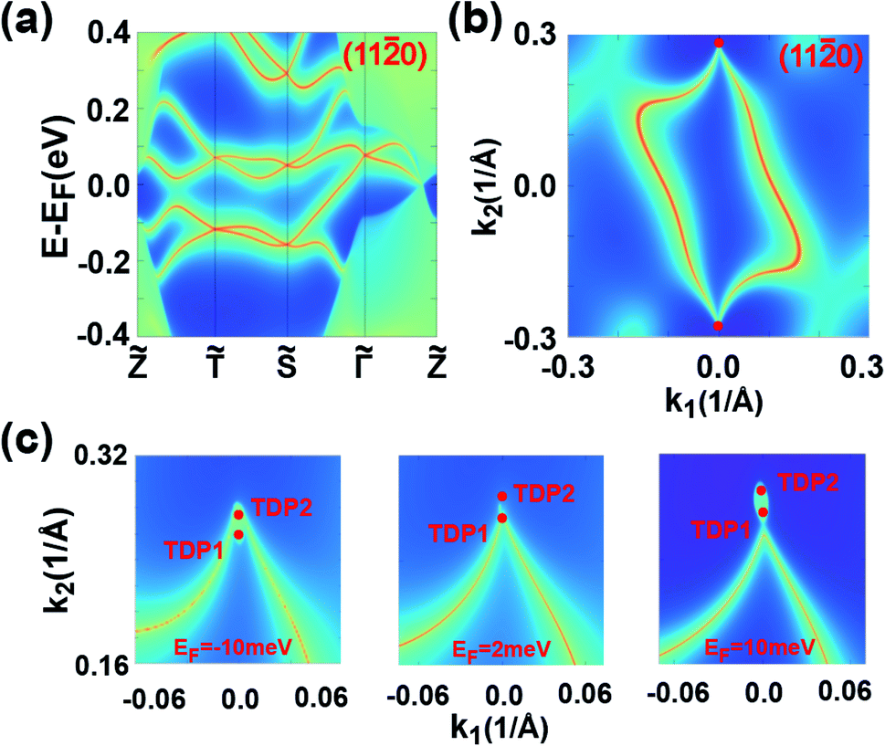 | ||
Fig. 4 (a) and (b) are the surface band structure and Fermi surface contour on the (110) plane of the C1 SnPbH2 crystal, respectively. (c) Fermi surfaces with different EFs for the (110) plane of the 3D SnPbH2 crystal. Two red dots in the magnified Fermi surfaces denote the surface projections of the two adjacent TDPs. k1 and k2 in (b) and (c) are the wave-vector units along the ![[capital Gamma, Greek, tilde]](https://www.rsc.org/images/entities/i_char_e1eb.gif) ![[S with combining tilde]](https://www.rsc.org/images/entities/i_char_0053_0303.gif) and and ![[Z with combining tilde]](https://www.rsc.org/images/entities/i_char_005a_0303.gif) directions, respectively. directions, respectively. | ||
We now explore the topological electronic structures of the C2 SnPbH2 crystal with space group P63mc. For the C2 configuration, the system has three important crystalline symmetries, including the mirror plane M (Fig. 1(b)), the glide-mirror plane (Fig. 1(b)), and the six-fold screw rotation S6z. The orbital-resolved band structure of the C2 SnPbH2 crystal in the presence of SOC is displayed in Fig. 5(a). Obviously, the system shows gapless semi-metallic behaviors around the EF, with the bands contributed by the Pb (and also Sn) s and p orbitals. Two crossing points around the EF along the high-symmetry line of Γ–A are labeled D1 and D2, as illustrated in Fig. 5(b). Because the crossing points are formed by two doubly degenerate bands, both D1 and D2 are gapless crossing points with quadruple degeneracy. By analyzing the orbital components, we find that the two crossing doubly degenerate bands are mainly composed of s and pz orbitals, and px,y orbitals of the Pb (and also Sn) atoms, respectively. Symmetry analysis shows that these two doubly degenerate bands belong to the Λ7 and Λ9 IRs of the C6v double group symmetry, respectively (Fig. 3(b)). Thus, two stable fourfold degenerate points (D1 and D2) arise from the band inversion between s, pz orbitals and px,y orbitals of the Pb (and also Sn) atoms, protected by the different symmetric properties of the Λ7 and Λ9 bands. As displayed in Fig. 5(b), the slopes of the two crossing bands at D1 have opposite signs, while the slopes of the two bands at D2 have the same sign, leading to D1 and D2 being type-I and type-II Dirac points, respectively. The double degeneracy of all bands along the Γ–A line in Fig. 5(b) stems from the anticommutation relation {S2z, M} = 0, where the S2z is contained in the S6z. If a uniaxial strain is applied to the system, the C6v symmetry is broken, leading to the coupling of the s, pz bands and the px,y bands. A strong topological insulating phase with indexes of (1; 000) can be obtained under this strain. In contrast to D1 and D2, D3 appears at the high-symmetry point A on the BZ boundary. Due to four degenerate orthogonal states coexisting at A, D3 is a degenerate quartet (see part C of the ESI†).
 | ||
| Fig. 5 (a) Band structure of the C2 SnPbH2 crystal SOC. The projected Pb and Sn atomic orbitals are also displayed. The sizes of the dots are proportional to the orbital contributions. (b) Amplified band structure of (a) along the high-symmetry line Γ–A. The Dirac points in (b) are labeled D1, D2, and D3, respectively. (c) and (d) are the surface band structure and Fermi surface contour on the (110) plane for the C2 SnPbH2 crystal, respectively. The dashed lines in (c) are used to guide the bandwidth of the hourglass cone. The red dots in (d) indicate the Dirac points. k1 and k2 in (d) are the wave-vector units along the and directions, respectively. | ||
We now take D1 as an example to analyze its topological nature. The obtained Z2 = 1 for the kz = 0 plane and Z2 = 0 for the kz = π plane indicate the topological nontriviality of D1. Fig. 5(c) and (d) show the surface bands and the Fermi surface contour for the (110) plane of the C2 SnPbH2 crystal, respectively. Different from the Dirac cone surface states,5 the (110) plane possesses very exotic characteristics due to the unique geometrical symmetries of the plane. On the (110) plane, the glide-mirror plane is preserved, giving rise to a surface fermion whose dispersion is shaped like an hourglass. The resultant hourglass surface state owns a relatively large bandwidth (about 80 meV) along the ![[T with combining tilde]](https://www.rsc.org/images/entities/i_char_0054_0303.gif) directions, defined as the smaller energy window between the two twofold degenerate points at the same time reversal invariant k point (denoted by the dashed lines in Fig. 5(c)). This value is several times the bandwidths of previously reported hourglass fermions in KHgX51 and other 3D bulk materials.52,53 The large bandwidth of the hourglass surface state favors detection using the standard angle-resolved photoemission spectroscopy (ARPES). The Fermi arc surface state of the C2 SnPbH2 crystal is displayed in Fig. 5(d), where the large and clear Fermi arcs can also be easily measured or confirmed by ARPES or scanning tunneling microscopy.
directions, defined as the smaller energy window between the two twofold degenerate points at the same time reversal invariant k point (denoted by the dashed lines in Fig. 5(c)). This value is several times the bandwidths of previously reported hourglass fermions in KHgX51 and other 3D bulk materials.52,53 The large bandwidth of the hourglass surface state favors detection using the standard angle-resolved photoemission spectroscopy (ARPES). The Fermi arc surface state of the C2 SnPbH2 crystal is displayed in Fig. 5(d), where the large and clear Fermi arcs can also be easily measured or confirmed by ARPES or scanning tunneling microscopy.
The electronic states and the topological properties of the 3D GeSnH2 and GePbH2 crystals are also investigated. The results are illustrated in part D of the ESI.† Among the ten typical stacking configurations, C1 and C2 are also found to be the two most stable configurations for both the 3D GeSnH2 and GePbH2 crystals. The electronic structures of the 3D GeSnH2 and GePbH2 crystals are somewhat different from those of the 3D SnPbH2 crystals. For example, the C1 and C2 3D GeSnH2 crystals are found to be normal insulators instead of the TDP or Dirac semimetals found in the SnPbH2 crystals, which can be rationalized well by the stronger nonmetallic property of Ge atoms than that of Pb atoms. The C1 GePbH2 crystal is found to be a weak topological insulator, with topological indexes of (0; 001) (Fig. 6(a) and (b)). The topologically nontrivial band gap at the EF is about 28.6 meV (Fig. 6(b)). Similar to the C1 SnPbH2 crystal, the two close TDPs (TDP3 and TDP4) form one “near-Dirac” point above the EF (Fig. 6(b) and (c)). The C2 GePbH2 crystal is a DSM with three Dirac points located around the EF (Fig. 6(d) and (e)). Thus, very abundant topological phases, including TDPSMs, DSMs (with different types), and weak topological insulators, etc., are achieved in the hydrogenated group-IVA binary compounds. This covalently functionalized honeycomb lattice may be expanded to many other 2D materials with different lattices or functionalized chemical groups,54–56 providing plenty of candidate materials for topologically nontrivial phases. The predicted multiple topological electronic states associated with multiple degrees of freedom of stacking configurations in the covalently functionalized honeycomb lattice pave a brand new way to develop novel quantum electronics with low power consumption and heat dissipation, and quantum computing free of decoherence.
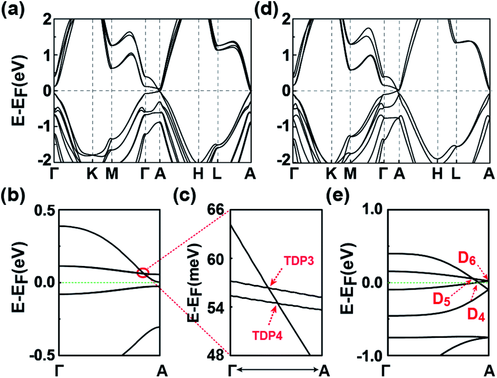 | ||
| Fig. 6 (a) Band structure of the C1 GePbH2 crystal with SOC. (b) Amplified band structure of (a) along the high-symmetry line Γ–A. (c) The amplified TDPs in (b), labeled TDP3 and TDP4, respectively. (d) and (e) are the same as (a) and (b), respectively, but for the C2 GePbH2 crystal. Three Dirac points in (e) are labeled D4, D5, and D6, respectively. | ||
4. Conclusions
In conclusion, using density-functional theory calculations and symmetry analysis, we predict a class of topological semimetal candidates in chemically modified group-IVA binary compounds. Topological semimetals are formed depending on the different stacking configurations. The C1 SnPbH2 crystal is a TDPSM, characterized by two sets of “near-Dirac” TDPs and protected by a C3v double point group symmetry. The origination of TDPs is understood by tuning the vdW interlayer space, which clearly demonstrates the band inversion between the s (pz) and px,y bands from the Pb (and also Sn) atoms. By changing the stacking configuration, a DSM with hourglass surface states is obtained in the C2 SnPbH2 crystal, featuring three kinds of Dirac points: one pair of clean type-I Dirac points located exactly at the EF and one pair of type-II Dirac points, and a single essential Dirac point occurring near the EF. The topological properties of the GeSnH2 and GePbH2 are also explored. The C1 and C2 GeSnH2 crystals are found to be normal insulators, while the C1 GePbH2 crystal turns out to be a weak topological insulator, and the C2 GePbH2 crystal a DSM with hourglass surface states. Our work reveals a new class of novel 2D materials hosting rich topological phases triggered by various stacking configurations, which serve as good candidates for promising topotronics.Author contributions
GG carried out the theoretical calculations with the assistance of HB, BZ, and HH. GG, BZ, and ZY analyzed the results. GG and ZY wrote the paper. ZY guided the project.Conflicts of interest
There are no conflicts to declare.Acknowledgements
This work was supported by the National Natural Science Foundation of China under Grants No. 11574051, No. 11604134, and No. 11874117. Most of the calculations were performed at the High Performance Computational Center (HPCC) of the Department of Physics at Fudan University.References
- M. Z. Hasan and C. L. Kane, Rev. Mod. Phys., 2010, 82, 3045 CrossRef CAS
.
- N. P. Armitage, E. J. Mele and A. Vishwanath, Rev. Mod. Phys., 2018, 90, 015001 CrossRef CAS
- P. Liu, J. R. Williams and J. J. Cha, Nat. Rev. Mater., 2019, 4, 479 CrossRef CAS
- X. L. Qi and S. C. Zhang, Rev. Mod. Phys., 2011, 83, 1057 CrossRef CAS
- Z. Wang, Y. Sun, X.-Q. Chen, C. Franchini, G. Xu, H. Weng, X. Dai and Z. Fang, Phys. Rev. B: Condens. Matter Mater. Phys., 2012, 85, 195320 CrossRef
- B. Bradlyn, J. Cano, Z. Wang, M. G. Vergniory, C. Felser, R. J. Cava and B. A. Bernevig, Science, 2016, 353, aaf5037 CrossRef PubMed
- S. M. Young, S. Zaheer, J. C. Y. Teo, C. L. Kane, E. J. Mele and A. M. Rappe, Phys. Rev. Lett., 2012, 108, 140405 CrossRef CAS PubMed
- X. Wan, A. M. Turner, A. Vishwanath and S. Y. Savrasov, Phys. Rev. B: Condens. Matter Mater. Phys., 2011, 83, 205101 CrossRef
- A. Bernevig, H. Weng, Z. Fang and X. Dai, J. Phys. Soc. Jpn., 2018, 87, 041001 CrossRef
- S. A. Parameswaran, T. Grover, D. A. Abanin, D. A. Pesin and A. Vishwanath, Phys. Rev. X, 2014, 4, 031035 CAS
- A. A. Burkov and Y. B. Kim, Phys. Rev. Lett., 2016, 117, 136602 CrossRef PubMed
- A. Chen, D. I. Pikulin and M. Franz, Phys. Rev. B: Condens. Matter Mater. Phys., 2017, 95, 174505 CrossRef
- C. Huang, B. T. Zhou, H. Zhang, B. Yang, R. Liu, H. Wang, Y. Wan, K. Huang, Z. Liao, E. Zhang, S. Liu, Q. Deng, Y. Chen, X. Han, J. Zou, X. Lin, Z. Han, Y. Wang, K. T. Law and F. Xiu, Nat. Commun., 2019, 10, 2217 CrossRef PubMed
- S.-Y. Xu, I. Belopolski, D. S. Sanchez, M. Neupane, G. Chang, K. Yaji, Z. Yuan, C. Zhang, K. Kuroda, G. Bian, C. Guo, H. Lu, T.-R. Chang, N. Alidoust, H. Zheng, C.-C. Lee, S.-M. Huang, C.-H. Hsu, H.-T. Jeng, A. Bansil, T. Neupert, F. Komori, T. Kondo, S. Shin, H. Lin, S. Jia and M. Z. Hasan, Phys. Rev. Lett., 2019, 116, 096801 CrossRef PubMed
- B. Q. Lv, S. Muff, T. Qian, Z. D. Song, S. M. Nie, N. Xu, P. Richard, C. E. Matt, N. C. Plumb, L. X. Zhao, G. F. Chen, Z. Fang, X. Dai, J. H. Dil, J. Mesot, M. Shi, H. M. Weng and H. Ding, Phys. Rev. Lett., 2015, 115, 217601 CrossRef CAS PubMed
- A. A. Soluyanov, D. Gresch, Z. Wang, Q. Wu, M. Troyer, X. Dai and B. A. Bernevig, Nature, 2015, 527, 495 CrossRef CAS PubMed
- Z. M. Zhu, G. W. Winkler, Q. S. Wu, J. Li and A. A. Soluyanov, Phys. Rev. X, 2016, 6, 31003 Search PubMed
- H. Weng, C. Fang, Z. Fang and X. Dai, Phys. Rev. B: Condens. Matter Mater. Phys., 2016, 93, 241202(R) CrossRef
- H. Huang, S. Zhou and W. Duan, Phys. Rev. B: Condens. Matter Mater. Phys., 2016, 94, 121117(R) CrossRef
- G. Chang, S.-Y. Xu, S.-M. Huang, D. S. Sanchez, C.-H. Hsu, G. Bian, Z.-M. Yu, I. Belopolski, N. Alidoust, H. Zheng, T.-R. Chang, H.-T. Jeng, S. A. Yang, T. Neupert, H. Lin and M. Z. Hasan, Sci. Rep., 2017, 7, 1688 CrossRef PubMed
- Z. K. Liu, B. Zhou, Y. Zhang, Z. J. Wang, H. M. Weng, D. Prabhakaran, S. –K. Mo, Z. X. Shen, Z. Fang, X. Dai, Z. Hussain and Y. L. Chen, Science, 2014, 343, 864 CrossRef CAS PubMed
- Z. K. Liu, J. Jiang, B. Zhou, Z. J. Wang, Y. Zhang, H. M. Weng, D. Prabhakaran, S.-K. Mo, H. Peng, P. Dudin, T. Kim, M. Hoesch, Z. Fang, X. Dai, Z. X. Shen, D. L. Feng, Z. Hussain and Y. L. Chen, Nat. Mater., 2014, 13, 677 CrossRef CAS PubMed
- J.-Z. Ma, J.-B. He, Y.-F. Xu, B. Q. Lv, D. Chen, W.-L. Zhu, S. Zhang, L.-Y. Kong, X. Gao, L.-Y. Rong, Y.-B. Huang, P. Richard, C.-Y. Xi, E. S. Choi, Y. Shao, Y.-L. Wang, H.-J. Gao, X. Dai, C. Fang, H.-M. Weng, G.-F. Chen, T. Qian and H. Ding, Nat. Phys., 2018, 14, 349 Search PubMed
- B. Q. Lv, Z.-L. Feng, Q.-N. Xu, X. Gao, J.-Z. Ma, L.-Y. Kong, P. Richard, Y.-B. Huang, V. N. Strocov, C. Fang, H.-M. Weng, Y.-G. Shi, T. Qian and H. Ding, Nature, 2017, 546, 627 CrossRef CAS PubMed
- Z. Wang, H. Weng, Q. Wu, X. Dai and Z. Fang, Phys. Rev. B: Condens. Matter Mater. Phys., 2013, 88, 125427 CrossRef
- Q. D. Gibson, L. M. Schoop, L. Muechler, L. S. Xie, M. Hirschberger, N. P. Ong, R. Car and R. J. Cava, Phys. Rev. B: Condens. Matter Mater. Phys., 2015, 91, 205128 CrossRef
- W. Gao, X. Zhu, F. Zheng, M. Wu, J. Zhang, C. Xi, P. Zhang, Y. Zhang, N. Hao, W. Ning and M. Tian, Nat. Commun., 2018, 9, 3249 CrossRef PubMed
- Z. Wang, D. Gresch, A. A. Soluyanov, W. Xie, S. Kushwaha, X. Dai, M. Troyer, R. J. Cava and B. A. Bernevig, Phys. Rev. Lett., 2016, 117, 056805 CrossRef PubMed
- A. K. Geim and I. V. Grigorieva, Nature, 2013, 499, 419 CrossRef CAS PubMed
- J. Zhang, B. Zhao, T. Zhou, Y. Xue, C. Ma and Z. Yang, Phys. Rev. B: Condens. Matter Mater. Phys., 2018, 97, 085401 CrossRef CAS
- X. Qian, J. Liu, L. Fu and J. Li, Science, 2014, 346, 1344 CrossRef CAS PubMed
- M. M. Otrokov, I. P. Rusinov, M. Blanco-Rey, M. Hoffmann, A. Yu. Vyazovskaya, S. V. Eremeev, A. Ernst, P. M. Echenique, A. Arnau and E. V. Chulkov, Phys. Rev. Lett., 2019, 122, 107202 CrossRef CAS PubMed
- J. Liu, H. Wang, C. Fang, L. Fu and X. Qian, Nano Lett., 2017, 17, 467 CrossRef CAS PubMed
- H. Zhang, C.-X. Liu, X.-L. Qi, X. Dai, Z. Fang and S.-C. Zhang, Nat. Phys., 2009, 5, 438 Search PubMed
- L. Huang, T. M. McCormick, M. Ochi, Z. Y. Zhao, M. T. Suzuki, R. Arita, Y. Wu, D. X. Mou, H. B. Cao, J. Q. Yan, N. Trivedi and A. Kaminski, Nat. Mater., 2016, 15, 1155 CrossRef CAS PubMed
- J. E. Padilha, R. B. Pontes, T. M. Schmidt, R. H. Miwa and A. Fazzio, Sci. Rep., 2016, 6, 26123 CrossRef CAS PubMed
- L. Liu, H. Qin and J. Hu, Sci. Rep., 2017, 7, 42410 CrossRef CAS PubMed
- S. J. Zhang, W. X. Ji, C. W. Zhang, S. S. Li, P. Li, M. J. Ren and P. J. Wang, RSC Adv., 2016, 6, 79452 RSC
- M. Q. Arguilla, S. Jiang, B. Chitara and J. E. Goldberger, Chem. Mater., 2014, 26, 6941 CrossRef CAS
- G. Kresse and J. Furthmüller, Phys. Rev. B: Condens. Matter Mater. Phys., 1996, 54, 11169 CrossRef CAS PubMed
- G. Kresse and D. Joubert, Phys. Rev. B: Condens. Matter Mater. Phys., 1999, 59, 1758 CrossRef CAS
- J. P. Perdew, K. Burke and M. Ernzerhof, Phys. Rev. Lett., 1996, 77, 3865 CrossRef CAS PubMed
- J. Klimes, D. R. Bowler and A. Michaelides, Phys. Rev. B: Condens. Matter Mater. Phys., 2011, 83, 195131 CrossRef
- T. J. Björkman, J. Chem. Phys., 2014, 141, 074708 CrossRef PubMed
- A. A. Mostofi, J. R. Yates, G. Pizzi, Y. S. Lee, I. Souza, D. Vanderbilt and N. Marzari, Comput. Phys. Commun., 2014, 185, 2309 CrossRef CAS
- Q. S. Wu, S. N. Zhang, H. F. Song, M. Troyer and A. A. Soluyanov, Comput. Phys. Commun., 2018, 224, 405 CrossRef CAS
- J. Heyd, G. E. Scuseria and M. Ernzerhof, J. Chem. Phys., 2003, 118, 8207 CrossRef CAS
- J. H. Jung, C.-H. Park and J. Ihm, Nano Lett., 2018, 18, 2759 CrossRef CAS PubMed
- R. Zacharia, H. Ulbricht and T. Hertel, Phys. Rev. B: Condens. Matter Mater. Phys., 2004, 69, 155406 CrossRef
- Z. Fang, H. Gao, J. W. F. Venderbos and A. M. Rappe, Phys. Rev. B: Condens. Matter Mater. Phys., 2020, 101, 125202 CrossRef CAS
- Z. Wang, A. Alexandradinata, R. J. Cava and B. A. Bernevig, Nature, 2016, 532, 189 CrossRef CAS PubMed
- B. Singh, B. Ghosh, C. Su, H. Lin, A. Agarwal and A. Bansil, Phys. Rev. Lett., 2018, 121, 226401 CrossRef PubMed
- S.-S. Wang, Y. Liu, Z.-M. Yu, X.-L. Sheng and S. A. Yang, Nat. Commun., 2017, 8, 1844 CrossRef PubMed
- S. S. Li, W. X. Ji, S. J. Hu, C. W. Zhang and S. S. Yan, ACS Appl. Mater. Interfaces, 2017, 9, 41443 CrossRef CAS PubMed
- Y. P. Wang, W. X. Ji, C. W. Zhang, P. Li, P. J. Wang, B. Kong, S. S. Li, S. S. Yan and K. Liang, Appl. Phys. Lett., 2017, 110, 233107 CrossRef
- M. H. Zhang, C. W. Zhang, P. J. Wang and S. S. Li, Nanoscale, 2018, 10, 20226 RSC
Footnote |
| † Electronic supplementary information (ESI) available: The stability of monolayer SnPbH2, various stacking configurations, the band structures based on the hybrid-functional methods for the C1 and C2 SnPbH2, the phonon spectra for the C1 and C2 SnPbH2, the symmetry analysis for the C2 SnPbH2, and the geometric and electronic structures for the 3D GeSnH2 and GePbH2. See DOI: 10.1039/d1ra01136g |
| This journal is © The Royal Society of Chemistry 2021 |