
 Open Access Article
 This Open Access Article is licensed under a Creative Commons Attribution-Non Commercial 3.0 Unported Licence
Development of a nanoscale electroless plating procedure for bismuth and its application in template-assisted nanotube fabrication†
Martin Christoph Scheuerlein * and
Wolfgang Ensinger
* and
Wolfgang Ensinger
Department of Materials and Earth Sciences, Technical University of Darmstadt, Alarich-Weiss-Str. 2, D-64287 Darmstadt, Germany. E-mail: scheuerlein@ma.tu-darmstadt.de
First published on 24th February 2021
Abstract
Electroless plating is a versatile technique for the facile and controlled synthesis of metallic thin films and nanostructures. While there are numerous known procedures involving transition metals, reports on the electroless plating of post-transition metals are particularly rare, even without considering specific nanofabrication requirements. In this work we outline the development of a remarkably stable electroless plating bath for nanoscale bismuth coatings, based on the reduction of Bi–EDTA by borane dimethylamine. Its suitability for nanostructure fabrication is showcased by coating ion-track etched polycarbonate membranes, creating Bi tubes with sub-micron diameters in the process. This procedure could be particularly useful for the development and improvement of high surface-area Bi based catalysts and heavy metal sensors.
Introduction
Electroless plating is a powerful and versatile tool, both in macroscale surface finishing and other applications such as microelectronics and nanostructure fabrication.1,2 The latter has seen increased research interest over the last decades, resulting in the development of nanoscale electroless plating procedures for a variety of metals and alloys.2,3 In its most simple form, an electroless plating bath consists of a metal precursor (usually complexed ions) and a reducing agent, which form a metastable redox pair. The reaction starts at a catalytically active surface and proceeds autocatalytically on the deposited film, while consuming the provided reducing agent. This sets it apart from galvanic exchange reactions, in which the dissolution of the substrate material provides the electrons for metal ion reduction.One of the main advantages of the technique is its technical simplicity, as many reactions can be performed under ambient conditions using basic laboratory equipment. Furthermore, it enables coating of a large variety of substrates, including insulators, as well as complex template geometries, such as nanostructured materials and porous membranes.4,5 Especially the ability to coat insulating surfaces is an advantage over electroplating.
In a variety of applications, bismuth is investigated as an environment-friendly alternative to its often highly toxic neighbours in the periodic table, especially lead and mercury.6,7 While being practically non-toxic, it shares some physical and chemical similarities with its peers, most notably a relatively low melting point (∼271.4 °C) and the ability to form eutectic alloys with a large variety of other heavy metals, such as Sn and Cd.8 This makes Bi, and in particular Bi nanostructures and thin films, a promising material class e.g. for replacing Pb in low-melting solders and Hg in heavy metal sensors.9,10 More recently, Bi nanostructures have also been investigated as catalysts for the reduction of CO2 to formate.11–13
While there are numerous studies on the autocatalytic electroless plating of various transition metals, reports on the deposition of main-group elements are rarely to be found. In the early 1990s, first electroless plating procedures for In, Sb, Pb and Bi were published, enabling the fast fabrication of micrometre sized films.14–17 In these cases, reduction of the precursor ions is achieved by using Sn(II)- and Ti(III)-complexes as reducing agents.17–19 However, the resulting deposits consist of large grains (multiple μm in size) and exhibit rough surfaces, while limitations in bath stability make them unsuitable for controlled nanoscale syntheses.
Other wet-chemical techniques for fabricating Bi containing thin films and nanostructures include electroplating and galvanic exchange reactions (sometimes also referred to as electroless plating), which, while offering good control over the film thickness and morphology, are limited to conductive substrates or result in the (partial) dissolution of the substrate material, respectively.20–25 Galvanic exchange reactions in particular have been used to fabricate Bi containing films, for example, on Si wafers,22 Al, Ag and Cu layers23,25 as well as Ni nanostructures.24 In these cases, however, the substrate actively takes part in the reaction, which means that these procedures are limited to certain suitable substrate materials and more importantly, inherently self-limiting as soon as a dense film is created. Additionally, the partial dissolution of the substrate can lead to the roughening of its surface and the incorporation of impurities into the final deposit.23
In this study, we outline the development of a facile, room-temperature electroless plating protocol for nanoscale Bi films. In contrast to the previously published procedures, reduction of Bi ions is achieved using dimethylamine borane (DMAB) as reducing agent, enabling a controlled deposition from a remarkably stable plating bath without dissolving the substrate. As substrate, ion-track etched polycarbonate (PC) membranes are used. In the context of the study, this serves a dual purpose: firstly, it showcases the nanofabrication potential of the presented plating procedure by offering a complex 3D substrate characterised by recessed, sub-micron diameter channels with high aspect-ratio. Secondly, it serves to demonstrate the possibility to create Bi coatings on polymer substrates, which is difficult, if not impossible with many of the existing wet-chemical procedures. Finally, the obtained thin-films and nanostructures are analysed by means of scanning electron microscopy (SEM), transmission electron microscopy (TEM), energy dispersive X-ray spectroscopy (EDS) and X-ray diffraction (XRD).
Experimental
Materials and methods
Prior to use, all glassware was cleaned with boiling aqua regia, stored in an alkaline bath for at least two days and subsequently washed with deionised water, prior to use. All aqueous solutions were prepared using high purity water (Milli-Q, >18.2 MΩ cm).The following chemicals have been used as obtained, without modification or further purification: bismuth(III) nitrate basic (Riedel-de-Haën, for analysis), ethylenediaminetetraacetic acid disodium salt dihydrate (EDTA, Sigma, ≥99% for electrophoresis), diethylenetriaminepentaacetic acid (DTPA, Fluka, ≥98%), nitrilotriacetic acid (NTA, Sigma-Aldrich, ≥99.0% puriss. p.a.), borane dimethylamine complex (DMAB, Aldrich, 97%), sodium hypophosphite (Sigma-Aldrich, ≥98% puriss.), hydrazine hydrate solution (Acros Organics, 80% in H2O), dichloromethane (Roth, ≥ 99.5%), tin(II) chloride dihydrate (Sigma-Aldrich, 98%), palladium(II) chloride (Aldrich, 99%), potassium chloride (PanReac Applichem, USP, Ph. Eur.), methanol (PanReac Applichem, pure), trifluoroacetic acid (Sigma-Aldrich, 99%).
Commercially available ion-track etched polycarbonate membranes were obtained from it4ip, Louvain-la-Neuve, Belgium. According to the manufacturer's specifications, they have a thickness of 25 μm with an areal pore density of 1.5 × 108 cm−2 and a pore diameter of 400 nm.
Sensitization and activation
For activation, Pd-seeds were deposited onto the polycarbonate membranes following a previously described two-step sensitisation and activation procedure.5 First, the membranes have been submerged in a Sn(II) containing solution (42 mM SnCl2, 71 mM trifluoroacetic acid in methanol and H2O (1![[thin space (1/6-em)]](https://www.rsc.org/images/entities/char_2009.gif) :1)) for 20 min. After rinsing with water, they were placed in a Pd(II) containing solution (11 mM PdCl2, 33 mM KCl in H2O) for 4 min. After washing with water, both steps were repeated two more times with the Sn(II) step shortened to 10 min. Finally, the membranes were washed in water and isopropanol and dried in air.
:1)) for 20 min. After rinsing with water, they were placed in a Pd(II) containing solution (11 mM PdCl2, 33 mM KCl in H2O) for 4 min. After washing with water, both steps were repeated two more times with the Sn(II) step shortened to 10 min. Finally, the membranes were washed in water and isopropanol and dried in air.
Synthesis of Bi(III)-complexes
The Bi(III)-complexes investigated in this study were prepared by suspending 10 mM of bismuth oxynitrate (BiONO3·H2O) in 11 mM aqueous solutions of the desired complexing agent (NTA, EDTA and DTPA). The suspension was stirred, and in the case of NTA and DTPA heated to 70 °C, until a clear solution was obtained.Electroless Bi deposition
The composition of the Bi–EDTA/DMAB plating bath is given in Table 1. All depositions using DMAB have been carried out at room temperature using the native pH of the solution (∼pH 6). When sodium hypophosphite and hydrazine were used as reducing agents, the concentrations (and pH values) were 200 mM (∼pH 8.5 by NaOH addition) and 480 mM (∼pH 9.5 by NaOH addition), respectively. Here, pH adjustments are necessary to ensure optimal plating conditions.26 In all cases, activated membranes were fixed vertically in the unstirred plating bath for the desired plating time. Afterwards, they were washed with water and isopropanol and dried in air. To reduce surface oxidation, samples were stored in a desiccator prior to characterisation.| Compound | Formula | Concentration | |
|---|---|---|---|
| Bi(III) source | Bismuth(III) oxynitrate (bismuth nitrate basic) | BiONO3·H2O | 10 mM |
| Complexing agent | Disodium ethylenediamine-tetraacetic acid (EDTA) dihydrate | Na2(H2edta)·2H2O | 11 mM |
| Reducing agent | Borane dimethylamine (DMAB) | (CH3)2NH·BH3 | 30 mM |
Characterisation
SEM and EDS measurements were carried out on a Philips XL30 FEG SEM with an attached EDAX CDU LEAP EDS detector. To analyse template-freed Bi nanotubes, the membranes were dissolved using dichloromethane (DCM). This was done by placing the sample on a Si wafer piece and applying a drop of DCM to fix it, before placing it in DCM for several hours until the solvent was evaporated.TEM measurements were performed on 70 nm thin microtome cuts of the metallised membranes. Prior to cutting, samples were embedded in Araldite® 502 resin (polymerization for 16 h at 60 °C). The obtained slices were placed on Cu-grids and analysed in a FEI CM20 TEM at an acceleration voltage of 200 kV.
XRD analysis was carried out on as-fabricated samples using a Seifert XRD 3003 PTS diffractometer with a Cu anode (40 kV, 40 mA). The Cu Kα radiation (λ ≈ 154.2 pm) is separated by a graphite monochromator and collimated on the secondary side using a long Soller slit. All measurements were performed in θ/2θ-geometry.
All UV-Vis measurements were performed on a VWR UV-3100PC spectrophotometer using Quartz-cuvettes. Due to their strong absorbance in the UV-range, Bi(III) containing solutions were diluted with water in a 1:100 ratio prior to the measurements.
Results and discussion
Development of an electroless Bi plating bath
In a typical electroless plating bath, the metal precursor (usually a complex ion) and reducing agent form a metastable redox pair, which only reacts on catalytically active surfaces and auto-catalytically on the deposited film. In the case of Bi the choice of a suitable precursor has to be carefully considered, as free Bi(III) ions easily hydrolyse in neutral and alkaline solutions, leading to the formation of insoluble Bi(OH)3 precipitates.27 Additionally, their comparatively high standard potential (Bi3+ + 3e− → Bi0; 0.308 V) makes them prone to homogeneous nanoparticle (NP) nucleation in the bulk solution when confronted with a reducing agent.8 Fortunately, it is well documented that Bi(III) forms remarkably stable and well water-soluble chelate-type complexes with (poly)amino-polycarboxylate ligands, such as NTA, EDTA and DTPA, which are investigated as possible Bi precursors in the present study.28,29 For each precursor solution, UV-Vis measurements show the characteristic absorption bands of the corresponding Bi(III) complex (Fig. 1a). The peak maxima are located at wavelengths of 243 nm, 264 nm and 277 nm for the NTA-, EDTA- and DTPA-compounds, respectively, which is in good accordance to previous reports.30–32 In the case of Bi–NTA, the characteristic absorbance at 243 nm suggests that a 1:1 (Bi:NTA) complex is formed.30 At the native pH values of the solutions, Bi–EDTA (∼pH 4.5) and Bi–DTPA (∼pH 1.5) likely exist as fully deprotonated ([Bi(edta)]−) and monoprotonated compounds ([Bi(Hdtpa)]−), respectively.28
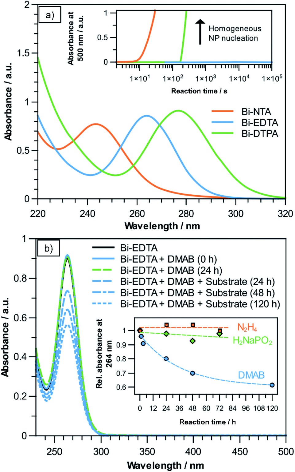 | ||
| Fig. 1 (a) UV-Vis spectra of solutions containing NTA-, DTPA- and EDTA-complexes of Bi(III). Inset: Absorbance at 500 nm after the addition of 100 mM DMAB, showing the onset of homogeneous NP formation using different complexing agents. (b) UV-Vis spectra of the Bi–EDTA plating solution before and after the addition of DMAB and the activated polycarbonate substrate, showing a decrease in Bi–EDTA concentration over time. Inset: Absorbance at 264 nm, relative to the initial value, after adding equally sized activated substrates, using different reducing agents. | ||
After adding 100 mM of the reducing agent DMAB, NTA- and DTPA-stabilized solutions turned opaque and black after a short time at room temperature, indicating the formation of Bi NPs. This obviously increases absorbance in the UV and visible spectra, which we used to determine the time it takes for bath decomposition to occur using these complexing agents. Observing the absorbance at 500 nm over time shows that using the Bi–NTA and Bi–DTPA compounds, bath decomposition occurs after roughly 60 s and 180 s, respectively (see inset Fig. 1a). Intriguingly, the Bi–EDTA/DMAB solution exhibits remarkable stability with regards to homogeneous NP formation, not showing any signs of degradation even after several days. The differences in bath stability correlate with the previously reported stability constants (logK) of the respective Bi-compounds, namely 18.2, 23.02 and 31.9 for [Bi(nta)], [Bi(Hdtpa)]− and [Bi(edta)]−, respectively.28 Due to its superior stability, Bi–EDTA is chosen as the Bi precursor for the subsequent deposition step. Additionally, since hydrolysis and subsequent Bi(OH)3 formation is unlikely to occur below pH 10,28 it is a promising candidate for electroless plating, as many conventional reducing agents like sodium hypophosphite (H2NaPO2) and hydrazine (N2H4) require alkaline environments for efficient plating reactions.26
In previously published electroless plating procedures for Bi, Sn(II)- and Ti(III)-complexes were used as reducing agents.17,19,33 In these cases, reduction of Bi(III) occurs by a simple electron transfer, resulting in the oxidation of the less noble metal complex. Compared to other commonly used reducers in electroless plating (e.g. N2H4, sodium hypophosphite or DMAB), no catalysed dehydrogenation of the compound is necessary.34 This results in a comparatively low activation energy of the reaction, making Sn(II)- and Ti(III)-complexes useful for plating of the catalytically less active post-transition metals. However, the comparatively fast plating speeds, limited bath stability and large grain sizes pose significant challenges in the context of controlled nanostructure fabrication. In order to address these problems, we investigated the possibilities of Bi(III) reduction using the aforementioned, more conventional reducing agents, despite the lower catalytic activity of Bi towards the decomposition of these compounds.
To initiate the reaction, a dense layer of Pd nanoparticles is applied to the substrate surface. Using a 10 mM [Bi(edta)]− solution, three common reducing agents (DMAB, hydrazine, sodium hypophosphite) were investigated for their suitability for electroless Bi plating. As exemplarily shown for DMAB in Fig. 1b, only adding the reducing agent does not change the intensity of the Bi–EDTA absorbance band at 264 nm, suggesting that no change in the coordination of Bi(III) takes place, even after 24 h. Adding the activated substrate results in the absorbance band of the Bi–EDTA complex becoming less intense over time, suggesting that Bi(III) is reduced and thus consumed during the plating reaction. This is supported by the apparent darkening of the substrate, turning the initial brownish colour of the Pd NPs more and more black over the course of the reaction. It is worth noting that no increase in absorbance in the visible spectrum can be observed, further corroborating that the reduction of Bi(III) is limited to the substrate surface and does not occur homogeneously in the plating solution. Assuming Lambert–Beer's law, the decrease in absorbance can be used to estimate the theoretical amount of deposited Bi, which in the present reaction (solution volume 10 mL, 100 mM DMAB, ∼pH 6) amounts to roughly 8.03 mg after 120 h of plating. This value agrees well with the recorded mass gain of the sample (∼7.98 mg), which both indicates a high efficiency of the plating reaction and further corroborates the absence of homogeneous NP formation in the bulk solution. The results suggest that in the given reaction conditions, DMAB is a suitable reducing agent for electroless Bi plating. An additional benefit of using DMAB is that the reaction can be performed in slightly acidic solutions, reducing the risk of Bi-oxide formation in the deposit.26 As the reaction progresses, it becomes slower, which is expected due to the decrease in both Bi–EDTA and DMAB concentrations, as well as the increasing coverage of Pd by the presumably less catalytically active Bi.35
A general, multi-step mechanism for the catalysed decomposition of DMAB and resulting metal reduction is given in the literature.34 Briefly, it can be described as a three-step dehydrogenation and oxidation process. In the first step, the metal surface facilitates the dissociation and dehydrogenation of DMAB (eqn (1)). The reaction product BH2OH− subsequently reacts with OH−, releasing an electron, which is then available for metal reduction (eqn (2)).34
 | (1) |
| ḂH2OH− + OH− → ḂH2(OH)2− + e− | (2) |
The resulting product then undergoes the same dehydrogenation and oxidation process two more times, ending with the metaborate anion (BO2−). The total reaction can be summarized as follows (eqn (3)).34
| 2[(CH3)2NH·BH3] + 8OH− → 2(CH3)2NH + 2BO2− + 4H2O + 3H2(↑) + 6e− | (3) |
It is important to mention, however, that this mechanism is usually proposed in the context of transition metal surfaces, such as the Pd seeds used to initiate the plating reaction in this study. We assume that a similar process also occurs on the deposited Bi layer, albeit with a much slower rate, due to the lower catalytic activity of Bi.
When hydrazine- or sodium hypophosphite-containing solutions are used (adjusted to ∼pH 9.5 and ∼pH 8.5, respectively), no overall decrease in Bi–EDTA absorbance can be observed even after 72 h, suggesting that little to no Bi plating takes place (see inset Fig. 1b). This might be attributed to the high stability of the Bi–EDTA complex and/or indicate a low catalytic activity of the electroless Bi deposits towards hydrazine and hypophosphite decomposition, preventing an autocatalytic plating reaction.
Characterisation of the obtained deposits
Plating reactions were carried out using the previously discussed Bi–EDTA/DMAB plating bath. Its composition is given in Table 1. Compared to the preliminary experiments, a lower DMAB concentration was chosen (30 mM instead of 100 mM) in order to decrease the plating speed and prevent a possible clogging of the membrane pores. The obtained deposits (24 h plating time) are analysed by SEM, TEM, EDS and XRD. SEM micrographs of the metallised membranes (Fig. 2a and b) show that the Bi deposit is thin and remarkably homogeneous. The complex geometry of the membrane is well reproduced, and the pores are still open and thus, accessible for potential catalytic or sensory applications. Measuring at the pore openings yields a film thickness of roughly 50 nm after 24 h of plating, which agrees well with the TEM data discussed later. After removal of the substrate by dissolution in dichloromethane (DCM), free-standing Bi tubes with lengths of several μm are obtained, their sub-micron diameter being determined by the pore size of the membrane (Fig. 2c and d). Due to the low wall thickness, however, structural support by the membrane is necessary to fully preserve their filigree shape.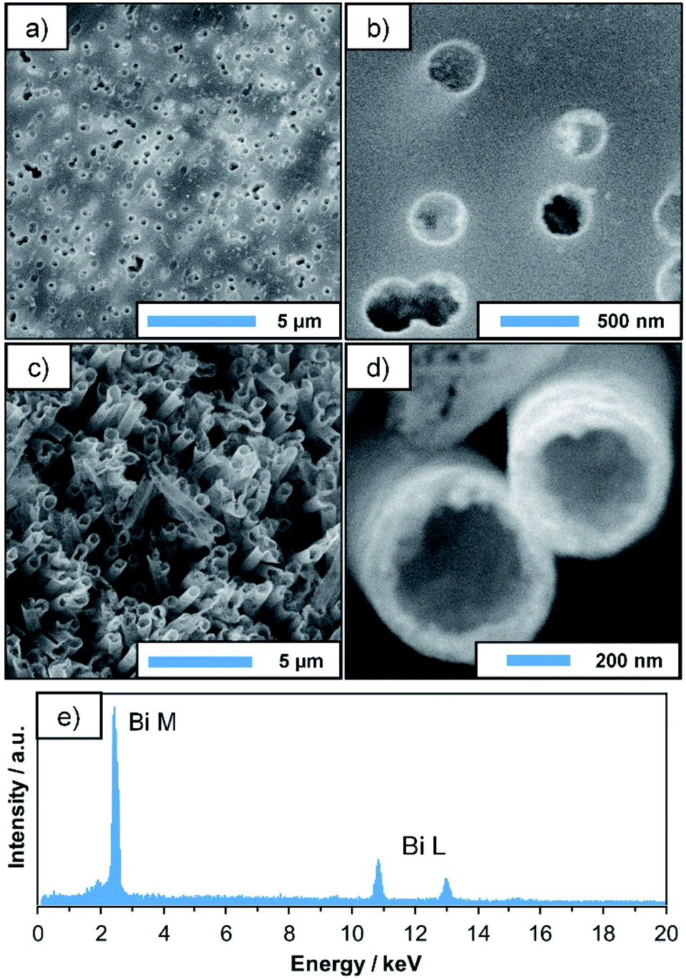 | ||
| Fig. 2 (a and b) SEM images of Bi coated ion-track etched PC membranes, revealing the smooth and homogeneous quality of the deposit. (c and d) Overview and detail images of sub-micron diameter Bi tubes obtained by dissolving the PC membrane after deposition. (e) EDS-spectrum of a typical electroless Bi-deposit, showing the dominating presence of Bi. Signals of B, O, Sn and Pd cannot be distinguished from the background. | ||
EDS measurements performed alongside SEM investigations confirm the dominating presence of Bi in the final deposit (Fig. 2e). Signals of B and O, which would hint at the formation of Bi borides and oxides, as well as Sn and Pd (which are used during the activation procedure) can barely be distinguished from the background, suggesting that the plated film consists mainly of pure Bi, with little contamination.
TEM investigations were performed on ultramicrotome cuts of the coated membrane, which was cut perpendicular (Fig. 3a and b) and parallel to the pore axis (Fig. 3c). In the first case, the statistically distributed, often overlapping metallised pores appear as dark ellipses (Fig. 3a). The deviation from the circular shape, which was observed in SEM, is due to the angle between the pore axes and the cutting-plane and/or the mechanical forces applied during the cutting process. A closer look reveals that the deposit consists of Bi NPs several tens of nm in size (Fig. 3b and c), which have grown on an underlying layer of smaller particles (Fig. 3d). Based on the TEM contrast and the vastly different particle size, we assume this to be the Pd seed layer applied in the activation step, which acts as a starting point for the autocatalytic deposition reaction. For comparison, a TEM image of an activated PC membrane (prior to Bi deposition) is presented in the ESI (Fig. S1†), showing a similar microstructure as the outer layer of the Bi tubes discussed above. Generally, the TEM images indicate a certain porosity of the Bi film, which could not be observed in SEM. While this might be an artifact of the sample preparation, in particular the cutting process, it makes it necessary to consider a second possible reaction mechanism in which the DMAB decomposition and oxidation only occurs on the still accessible Pd seeds, transferring electrons to the Bi particles and thus enable further Bi deposition. This would in turn cause the reaction to be self-limiting, as it would stop as soon as a dense Bi layer is formed. However, with increasing deposition times and DMAB concentrations, thicker and denser films can be obtained, which suggests that the reaction indeed continues autocatalytically on the deposited Bi film (see ESI, Fig. S2†). This is particularly interesting, as in a previous report, Bi particles produced in a gas phase reaction did not show catalytic activity towards DMAB decomposition.35 In the same study, however, it was shown that in the case of Ni the method of preparing the seed particles drastically influences the catalytic activity of their surface. While Ni particles created by gas-phase methods were inactive towards the reaction, chemically deposited Ni showed high catalytic activity. It is possible that in the case of Bi a similar phenomenon occurs, where certain impurities specific to the chemical process (e.g. B), or simply the absence of an oxide layer enable or even promote DMAB decomposition. Nonetheless, a detailed mechanistic study on this aspect is necessary in order to better understand these complex interface phenomena.
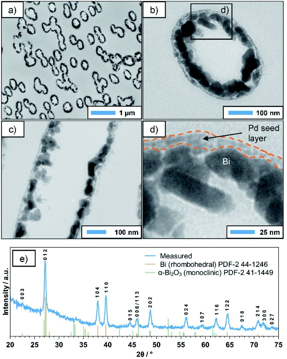 | ||
| Fig. 3 TEM images of (a) a cross-section of the metallised membrane (perpendicular to pore axis), highlighting the statistical distribution of pores. (b and c) Close-up images of cross-sections perpendicular and parallel to the pore axis, respectively, revealing the granular microstructure of the deposit. (d) Detail of a metallized pore-wall, showing the interface between the Pd seed layer and Bi crystallites. (e) XRD pattern indicating that the deposit consists mainly of the rhombohedral phase of Bi. The amorphous background at smaller scattering angles is caused by the underlying PC membrane. | ||
The XRD pattern of the deposit (Fig. 3e) corresponds well to the rhombohedral phase of Bi. The small additional peak around 33.5° might be caused by superficial oxide species resulting from the sample being stored in air, while the amorphous background at smaller angles can be attributed to the underlying PC membrane. Interestingly, the pronounced and relatively sharp reflexes suggest a high crystallinity of the deposited layer. While some DMAB-based plating baths (e.g. for Ni and Co) result in the deposition of nanocrystalline or even amorphous metal borides,5 this seems not to be the case here. This indicates that possible B incorporations resulting from the use of DMAB as a reducer do not significantly alter the rhombohedral Bi lattice. Applying Scherrer's equation to the (110) reflex suggests an average grain size of roughly 40 nm, which is in good agreement to the particle sizes observed in TEM (Fig. 3). Overall, the data strongly suggests that during the deposition reaction, crystalline, rhombohedral Bi is deposited predominantly.
Conclusions
The results show that nanoscale electroless Bi plating is possible using a comparatively simple, yet highly stable, three-component bath. The necessary metastability of the solution can be achieved by combining the remarkably stable Bi–EDTA complex with borane dimethylamine as a reducer. The obtained deposits are conformal and homogeneous, despite the complex substrate structure, and consist of crystalline, rhombohedral Bi. Removing the membrane after the deposition produces Bi tubes with sub-micron diameters and lengths of several micrometres. While the process can certainly be optimized by further studies focusing on the reaction mechanism and deposition parameters, we feel that the ability to coat complex nanostructured substrates opens up promising possibilities for the efficient use of Bi in high surface-area catalysts (e.g. for CO2 reduction) and electrodes (e.g. for heavy metals sensing).4,10–13,21 As the presented plating reaction only occurs on catalytically active surfaces, it might also be interesting for applications in which surface selective Bi coating is desired, for example during the application of solders in microelectronics.22,24Conflicts of interest
There are no conflicts to declare.Acknowledgements
The authors highly appreciate TEM measurements performed by Ulrike Kunz (FG Physikalische Metallkunde, TU Darmstadt). Access to the XRD setup was kindly provided by the structure research group (FG Strukturforschung) at TU Darmstadt. M. C. S. is grateful for valuable discussion with Falk Muench and Tim Boettcher (FG Materialanalytik, TU Darmstadt) and for financial support through Deutsche Forschungsgemeinschaft (DFG) grant number 406700532.Notes and references
- G. O. Mallory and J. B. Hajdu, Electroless Plating: Fundamentals and Applications, Cambridge University Press, Cambridge, 1990 Search PubMed.
- C. R. K. Rao and D. C. Trivedi, Coord. Chem. Rev., 2005, 249, 613–631 CrossRef CAS.
- C. N. Grabill, D. Freppon, M. Hettinger and S. M. Kuebler, Appl. Surf. Sci., 2019, 466, 230–243 CrossRef CAS.
- F. Muench, Catalysts, 2018, 8, 597 CrossRef.
- S. Schaefer, E.-M. Felix, F. Muench, M. Antoni, C. Lohaus, J. Brötz, U. Kunz, I. Gärtner and W. Ensinger, RSC Adv., 2016, 6, 70033–70039 RSC.
- A. A. Plionis, S. R. Garcia, E. R. Gonzales, D. R. Porterfield and D. S. Peterson, J. Radioanal. Nucl. Chem., 2009, 282, 239–242 CrossRef CAS.
- K. Vytřas, I. Švancara and R. Metelka, Electroanalysis, 2002, 14, 1359–1364 CrossRef.
- W. M. Haynes, D. R. Lide and T. J. Bruno, CRC Handbook of Chemistry and Physics, CRC Press, Boca Raton, 95th edn, 2014 Search PubMed.
- W. R. Osório, L. C. Peixoto, L. R. Garcia, N. Mangelinck-Noël and A. Garcia, J. Alloys Compd., 2013, 572, 97–106 CrossRef.
- J. Wang, Electroanalysis, 2005, 17, 1341–1346 CrossRef CAS.
- K. Fan, Y. Jia, Y. Ji, P. Kuang, B. Zhu, X. Liu and J. Yu, ACS Catal., 2020, 10, 358–364 CrossRef CAS.
- S. X. Guo, Y. Zhang, X. Zhang, C. D. Easton, D. R. MacFarlane and J. Zhang, ChemSusChem, 2019, 12, 1091–1100 CrossRef CAS.
- N. Han, Y. Wang, H. Yang, J. Deng, J. Wu, Y. Li and Y. Li, Nat. Commun., 2018, 9, 1320 CrossRef.
- A. Senda, Y. Takano and T. Nakagawa, J. Surf. Finish. Soc. Jpn., 1992, 43, 694–699 CrossRef CAS.
- A. Senda, Y. Takano and T. Nakagawa, J. Surf. Finish. Soc. Jpn., 1992, 43, 589–594 CrossRef CAS.
- A. Senda, T. Nakagawa, Y. Takano and T. Kasanami, J. Surf. Finish. Soc. Jpn., 1992, 43, 324–329 CrossRef CAS.
- A. Senda, Y. Takano and T. Nakagawa, J. Surf. Finish. Soc. Jpn., 1993, 44, 145–150 CrossRef CAS.
- D. L. Rutkevich, G. P. Shevchenko, V. V. Sviridov and N. P. Osipovich, J. Electrochem. Soc., 1993, 140, 3473–3478 CrossRef CAS.
- E. Uchida, K. Tanaka, M. Okada, T. Tsuruoka, K. Akamatsu and H. Nawafune, Trans. Mater. Res. Soc. Jpn., 2014, 39, 47–51 CrossRef CAS.
- T. W. Cornelius, J. Brötz, N. Chtanko, D. Dobrev, G. Miehe, R. Neumann and M. E. Toimil Molares, Nanotechnology, 2005, 16, S246–S249 CrossRef CAS.
- Z. Zhang, K. Yu, D. Bai and Z. Zhu, Nanoscale Res. Lett., 2010, 5, 398–402 CrossRef CAS.
- T. Romann, E. Anderson, S. Kallip, H. Mändar, L. Matisen and E. Lust, Thin Solid Films, 2010, 518, 3690–3693 CrossRef CAS.
- S. S. Djokić, K. Prashanthi and T. Thundat, Electrochem. Solid-State Lett., 2012, 15, 2012–2014 CrossRef.
- A. Danine, K. Termentzidis, S. Schaefer, S. Li, W. Ensinger, C. Boulanger, D. Lacroix and N. Stein, Superlattices Microstruct., 2018, 122, 587–595 CrossRef CAS.
- S. S. Djokić, N. S. Djokić and T. Thundat, J. Electrochem. Soc., 2012, 159, D587–D591 CrossRef.
- I. Ohno, O. Wakabayashi and S. Haruyama, J. Electrochem. Soc., 1985, 132, 2323 CrossRef CAS.
- G. K. Schweitzer and L. L. Pesterfield, The Aqueous Chemistry of the Elements, Oxford University Press, Inc., New York, 2010 Search PubMed.
- V. Stavila, R. L. Davidovich, A. Gulea and K. H. Whitmire, Coord. Chem. Rev., 2006, 250, 2782–2810 CrossRef CAS.
- D. Kruk, E. Umut, E. Masiewicz, P. Hermann and H. Scharfetter, Mol. Phys., 2018, 117, 927–934 CrossRef.
- B. P. Karadakov and D. I. Venkova, Talanta, 1970, 17, 878–883 CrossRef CAS.
- W. R. Harris, Y. Chen, J. Stenback and B. Shah, J. Coord. Chem., 1991, 23, 173–186 CrossRef CAS.
- W. Liao, P. Lei, J. Pan, C. Zhang, X. Sun, X. Zhang, C. Yu and S.-K. Sun, Biomaterials, 2019, 203, 1–11 CrossRef CAS.
- D. L. Rutkevich, G. P. Shevchenko, V. V. Sviridov and N. P. Osipovich, J. Electrochem. Soc., 1993, 140, 3473–3478 CrossRef CAS.
- J. E. A. M. Van Den Meerakker, J. Appl. Electrochem., 1981, 11, 395–400 CrossRef CAS.
- M. Lelental, J. Electrochem. Soc., 1973, 120, 1650 CrossRef CAS.
Footnote |
| † Electronic supplementary information (ESI) available: Additional TEM images. See DOI: 10.1039/d1ra00978h |
| This journal is © The Royal Society of Chemistry 2021 |