
 Open Access Article
 This Open Access Article is licensed under a Creative Commons Attribution-Non Commercial 3.0 Unported Licence
Studies on structural, dielectric and optical properties of (Ba0.95Ca0.05)1−x(Ti0.8Sn0.2)1−xNaxNbxO3 lead-free ceramics
H. Slimi *a,
A. Oueslatib and
A. Aydia
*a,
A. Oueslatib and
A. Aydia
aLaboratory of Multifunctional Materials and Applications (LaMMA), LR16ES18, Faculty of Sciences of Sfax, University of Sfax, BP 1171, 3000 Sfax, Tunisia. E-mail: slimi.houda1@gmail.com
bLaboratory of Spectroscopic Characterization and Optic Materials, University of Sfax, Faculty of Sciences of Sfax, B.P. 1171, 3000 Sfax, Tunisia
First published on 19th April 2021
Abstract
(Ba0.95Ca0.05)1−x(Ti0.8Sn0.2)1−xNaxNbxO3 (BCNTSNO3) lead-free ceramics with compositions (x = 0.75, 0.8 and 0.85) were synthesized through the traditional solid-state reaction method. X-ray powder diffraction analysis showed the formation of a single phase compound crystallized in tetragonal space group P4mm. The evolution of Raman spectra displayed a disorder introduced into the structure, which favors a ferroelectric relaxor behavior. The dependence of the dielectric properties on temperature exhibited two composition ranges with different behaviors. Ferroelectric relaxor properties were observed for the compositions x < 0.85 and the classical ferroelectric behavior for x = 0.85. Lead free (Ba0.95Ca0.05)1−x(Ti0.8Sn0.2)1−xNaxNbxO3 ceramics exhibited larger dielectric constants than those of parent crystal NaNbO3, suggesting that it is a good candidate for lead-free ceramics in several industrial applications. Using UV-Vis spectroscopy, the optical band gap energy of ceramics (Ba0.95Ca0.05)1−x (Ti0.8Sn0.2)1−xNaxNbxO3 is found at 2.89, 2.92, and 3.05 eV for x = 0.75, 0.8 and 0.85, respectively.
1. Introduction
With the recent growing demand for global environmental protection and sustainable development, researchers' interests have turned to lead-free materials such as ferroelectrics with the ABO3 perovskite structure.1–3 Due to their multifunctional properties,4–6 good thermal resistance as well as chemical stability, nature-friendly ferroelectrics may be good candidates for industrial applications. These materials have similar or better physicochemical properties than toxic ferroelectrics. Ferroelectrics are typical materials that exhibit spontaneous polarization, in which their direction is reversed by reversing the external electric field. However, based on their behavior, ferroelectric materials have been extensively used in multiple fields including multilayer capacitors, electromechanical systems, energy storage and ultrasonic transducers.7–11 Recently, the coupling of ferroelectric polarization with light absorption makes the ferroelectric perovskites promising candidates for applications in photoelectrics.12Barium titanate (BaTiO3) is a classical ferroelectric used for the preparation of ceramics, which is widely explored given its excellent electrical, dielectric and ferroelectric properties. From the viewpoint of the nature of ferroelectric phase transitions between order-disorder and displacive scenarios, it presents a very large optical band gap energy of about 3.26 eV.13 In attempts to improve the properties of BaTiO3, dopants are generally added to the A and/or B sites of the material. In this case, the BaTiO3–CaTiO3–BaSnO3 ternary system was studied.14 The latter may display multiphase coexistence at room temperature such as a Morphotropic phase boundary (MPB) or polymorphic phase boundary (PPB), where good piezoelectric property is expected with a high value of TC.
Sodium niobate NaNbO3 (NN) is an antiferroelectric (AFE) perovskite with an orthorhombic structure in space group Pbma at room temperature.15 It has attracted attention owing to its successive phases structure transition.16 In addition, NaNbO3 perovskite is an important photocatalysis semiconductor with a band gap energy of 3.4 eV.17,18 As a result, NN is also a promising candidate in many areas of optical applications involving energy storage, optical waveguides, ultrafast optical switching, non-volatile ferroelectric memories and semiconductor photoélectrodes.19 Moreover, in the field of photocatalysis, it is used for the separation of water, purifying the air and the decomposition of dyes.20,21 Furthermore, the dielectric behavior of NN has been widely investigated. It exhibits a phase transition at TC around 913 K with a maximum real permittivity of  1750 at TC.22 NaNbO3 (NN) is a anti-ferroelectric at room temperature17 and it transforms to ferroelectric substance, if mixed with a small amount of KNbO3,7 LiNbO3,23 BaSnO3,24 and SrSnO3.25 However, only several studies have been conducted on the ceramics formed BaTiO3–NaNbO3 system with the aim to examine the effect of cation substitution in A and B sites, including significant changes in the dielectric and structural properties.
The mixture or solid solution of anti-ferroelectric and ferroelectric materials usually results in the formation of multifunctional material having good ferroelectric and piezoelectric properties.26 In this study, antiferroelectric NN and ferroelectric ternary systems BaTiO3–CaTiO3–BaSnO3 are synthesized to develop a new lead free ferroelectric solid solution with general composition (1 − x)[(Ba0.95Ca0.05)(Ti0.8Sn0.2)] NaxNbxO3. The ceramics (Ba0.95Ca0.05)1−x(Ti0.8Sn0.2)1−xNaxNbxO3 with x = 0.75, 0.8 and 0.85 were synthesized by means of the conventional solid-state reaction method. The structural and physical properties were explored by X-ray diffraction, dielectric measurements and Raman spectroscopy. The optical properties under UV-visible irradiation were reported.
2. Experimental details
The compounds (Ba0.95Ca0.05)1−x(Ti0.8Sn0.2)1−xNaxNbxO3, (x = 0.75, 0.8 and 0.85), were prepared through the conventional solid-state reaction method. The used precursors are as follows: carbonates (BaCO3, CaCO3 and Na2CO3) and oxides (SnO2, TiO2 and Nb2O5) with 99.9% purity of Aldrich brand. The mixed powders are milled in an agate mortar for 1 hour to homogenize the mixture and reduce the size of the grain size. The homogenized powders are calcined between 1000 and 1100 °C for 12 h in an electric furnace to evaporate CO2. The calcined powders are ground, again for 1 h and then shaped into pellets of 8 mm in diameter and 1 mm thick to undergo second heat treatment (sintering) at a higher temperature ranging between 1250 and 1400 °C for 2 h.To examine the phase purity and evolution of the crystal symmetry of the prepared ceramics, the X-ray diffraction measurements were carried out on sintered pellets at room temperature. The intensity determining was performed by a step of 0.02 in 2θ and a counting time of 10 s by means of a Philips X'pert PW 3040/00 diffractometer using the Kα radiation (λ = 1.5406 Å). Cell parameters and line profile were refined by a global method using the Fullprof program based on Rietveld method.27
The dielectric study was carried out on sintered pellets of diameter 7 mm and thickness 1 mm. The impedance spectroscopy measurements were performed as a function of temperature (50–600 K) and frequency (0.1 Hz to 200 kHz) using a Wayne-Kerr 6425 component analyzer.
The Raman spectra were recorded in the wavenumber range of 50–1000 cm−1 on a Horiba Lab-ram HR 800 Raman spectrometer equipped with a He–Ne laser of 633 nm emission line with the power of 15 mW and a CCD detector.
The linear optical properties were measured at room temperature, using a UV-3101PC scanning spectrophotometer in the 200–1000 nm wavelength range.
3. Results and discussion
3.1 X-ray diffraction analysis
The X-ray patterns of (Ba0.95Ca0.05)1−xNax(Ti0.8Sn0.2)1−xNbxO3 ceramics of compositions (x = 0.75, 0.8 and 0.85) indicate that all the samples have pure perovskite-type structures without secondary phases, implying that the Ba2+, Ca2+, Sn4+, and Ti4+ ions are well incorporated on the A and B sites of NaNbO3 lattice. The Rietveld refinements of the XRD patterns exhibit a tetragonal phase with space group P4mm at room temperature. This symmetry is characterized by a (002)/(200) peak splitting between 45° and 46°. As an example, the difference diffraction pattern for x = 0.75 is shown in Fig. 1.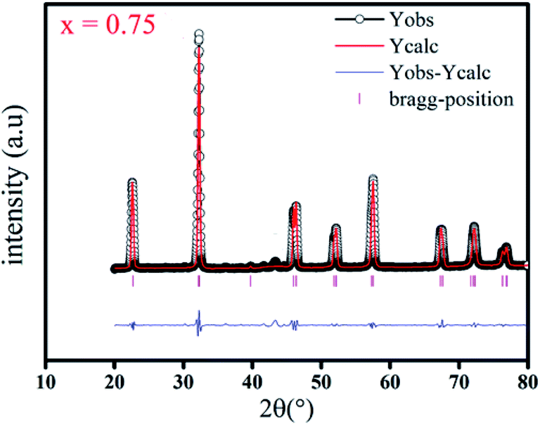 | ||
| Fig. 1 X-ray diffraction pattern at room temperature of BCNTSNO ceramic with composition corresponding to x = 0.75. | ||
The corresponding results and the estimated values of the refinement parameters of the title ceramics are summarized in Table 1. One can notice that, when x increases, the cell parameters a, b, c and cell volume v increase. These results can be related to the increase of the ionic radii of the cations substituted in A and B sites.
| (Ba0.95Ca0.05)1−xNax(Ti0.8Sn0.2)1−xNbxO3 | X = 0.75 | X = 0.8 | X = 0.85 |
|---|---|---|---|
| Phase | Tetragonal | Tetragonal | Tetragonal |
| Space group | P4mm | P4mm | P4mm |
| Lattice parameters | a = b = 3.916 Å | a = b = 3.919 Å | a = b = 3.924 Å |
| c = 3.946 Å | c = 3.9447 Å | c = 3. 945 Å | |
| v = 60.498 Å3 | v = 60.567 Å3 | v = 60.685 Å3 | |
| 〈rA〉 | 1.279 | 1.259 | 1.239 |
| 〈rB〉 | 0.635 | 0.637 | 0.638 |
| t | 0.924 | 0.917 | 0.910 |
The values of the ionic radii (rNa+) = 1.18 Å and (rNb5+) = 0.64 Å coordinated with 8 and 6 respectively for NN lower than those of (rBa2+) = 1.61 Å, (rCa2+) = 1 Å, (rSn4+) = 0.69 Å and (rTi4+) = 0.605 Å in coordination with 6 in BTS.28 Moreover, these results are in relation with the variations of the average radii in site A 〈rA〉 and in site B 〈rB〉. The following relations govern these radii:
| 〈rA〉 = x(rNa+) + (1 − x)[0.95(rBa2+) + 0.05(rCa2+)] |
| 〈rB〉 = x(rNb5+) + (1 − x)[0.8(rTi4+) + 0.2(rSn4+)] |
According to the calculations, we notice that the ionic radius 〈rA〉 decreases from 1.27 to 1.239 Å, respectively, for x = 0.75 and 0.85. As it appears, in this case, the ionic radius in A site should increase. However, the ionic radius 〈rB〉 of the B-site increases with a small step from 0.635 to 0.638 Å. Therefore, the increase of the lattice parameters as well as the cell volume as a function of compositions could be accounted for in terms of the increase of 〈rB〉 rather than 〈rA〉.
It is interesting to find out the regularities, which govern the formation of perovskite compounds and use them to further guide the exploration of new materials. In the early 1920s, Goldschmidt29 proposed a tolerance factor “t” to study the stability of perovskite, defined as:
 | (1) |
3.2 Raman spectroscopy
The Raman spectra of the BCNTSNO ceramics at various compositions (x = 0.75, 0.8 and 0.85) at room temperature, were measured to further explore the evolution of the structure of BCNTSNO ceramics, as shown in Fig. 2. | ||
| Fig. 2 Room temperature Raman spectra of (Ba0.95Ca0.05)1−xNax(Ti0.8Sn0.2)1−xNbxO3 ceramics with x = 0.75, 0.8 and 0.85 compositions. | ||
The presence of three mains regions, which are detected in the parent compounds BaTiO3 and NaNbO3 is evident in Fig. 2.30,31 The region (I), the modes at wavenumbers <170 cm−1 is associated with external vibrations of NbO6 octahedron, which is connected to the vibrations of the perovskite A-site). The region (II), the 170–450 cm−1 modes related to O–Nb–O bending; zone (III), the 450–800 cm−1 host modes related to the NbO6 octahedral vibrations. These two regions are attributed to the internal vibration of the NbO6 octahedron. To get the accurate change affected in the position, intensity and half-width of all bands with the increasing of x, Raman spectra are fitting with Fityk program, using pseudo-Voigt function. An example of the Raman spectrum fitting for x = 0.75 in the 50–1000 cm−1 spectral range is given in Fig. 3. The assignments of principal bands are reported in Table 2.
 | ||
| Fig. 3 Deconvolution of Raman spectra of the BCNTSNO0.75 ceramic at room temperature. | ||
| NaNbO3 (ref. 31) | Ba0.1(Sn0.5Ti0.5)0.1Na0.9Nb0.9O3 (ref. 34) | Assignments | |||
|---|---|---|---|---|---|
| x = 0.75 | x = 0.8 | x = 0.85 | |||
| 64 | 62 | 60 | 60.0 | 61 | Na+ |
| — | — | 66 | 66 | 66 | Na+ |
| 76 | — | 70 | 71 | 75 | Na+ |
| — | — | — | — | — | |
| 95 | — | — | 84 | — | |
| — | — | 99 | 100 | 101 | Na+ |
| 126 | 105 | — | — | — | |
| — | — | — | |||
| 146 | |||||
| — | — | 143 | 145 | 144 | Ba2+ |
| 157 | 154 | — | — | — | |
| — | — | — | — | ||
| 180 | — | 173 | 174 | 177 | ν6 (Nb–O) |
| — | — | — | — | — | |
| 186 | — | — | — | — | |
| — | — | ||||
| 223 | 222 | 215 | 214 | 219 | ν5 (Nb–O) |
| 258 | 240 | 257 | 262 | 263 | |
| 279 | 275 | — | — | — | |
| 375 | — | 311 | 324 | 326 | E(TO + LO) |
| 433 | 430 | 441 | 445 | 434 | ν4 (Nb–O) |
| 560 | — | 551 | 552 | 561 | ν2 (Nb–O) |
| — | |||||
| 605 | 601 | 598 | 601 | 606 | ν1 (Nb–O) |
| 867 | 835 | 849 | 863 | ν1 + ν5(Sn–O) | |
The bands situated between 60–101 cm−1 are related to Na+ translational movements, while the vibrational band located at 144 cm−1 is associated with the Ba2+ stretching vibration.32 A small shift in the intensity and frequency is observed for these bands with increasing composition x.
Accordingly, the Raman modes observed at approximately 177 and 263 cm−1 are attributed to the ν6 and ν5 modes, respectively, which are in turn assigned to the (Nb–O) bending vibration of the NbO6 octahedra. Moreover, the existence of the mode B1 + E(TO + LO) around 326 cm−1 confirmed the presence of the tetragonal phase in all ceramics, as was detected by XRD studies.33 The band detected at 434 cm−1 is related to asymmetric bending vibration ν4(Nb–O).25 However, the intense Raman band of the prepared lead-free ceramics in the 598–606 cm−1 region corresponds to a shoulder in the 551–561 cm−1 region. These bands ν1 are and ν2 are assigned to symmetric and asymmetric stretching modes of the NbO6 octahedra. Finally, the mode at 863 cm−1 is attributed to ν1 + ν5 vibration modes combination, associated with the Sn–O stretching vibration.31 A most significant change is observed in the characteristics of the internal bands on increasing the degree of substitution, except for the increased splitting and shifting of the peak on the right side to higher frequencies. Also, we notice that these bands become more broadening with the increase of the composition x, which implied that the internal mode was sensitive to the effect of substitution in the NaNbO3.
Additionally, it can also be seen from the Raman spectra that with incasing the composition x, no peaks are observed indicating the absence of formation of a new phase and consequently the formation of solid solutions, which confirms the results found by DRX. When the composition x increases, all the bands display a decreasing intensity and shifted to the high frequency. This behavior can be connected with the disorder of ionic charge created on the A and B sites of NaNbO3 and distortion of NbO6 octahedra, as a consequence of Ba, Ca, Sn, and Ti substitutions.
3.3 Dielectric study
The dependence of relative permittivity of (Ba0.95Ca0.05)1−x(Ti0.8Sn0.2)1−xNaxNbxO3 ceramics for x = 0.75, 0.8 and 0.85 on temperature at some particular frequencies is illustrated in Fig. 4a and b. The dielectric characterization of the prepared ceramics shows an evolution from relaxor ferroelectric behavior to a classic ferroelectric under the effect of the degree of substitution of the cation Na2+ by (Ba2+, Ca2+) and Nb5+ by (Ti4+, Sn4+) in A and B sites, respectively. Meanwhile, for all the prepared lead-free ceramics a signal dielectric peak is observed, corresponding to ferroelectric paraelectric transition.
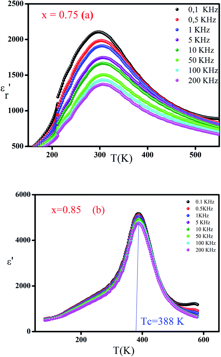 | ||
Fig. 4 Thermal variation of the real part  of the dielectric permittivity of (Ba0.95Ca0.05)1−xNax(Ti0.8Sn0.2)1−xNbxO3 with compositions at different frequencies (a) x = 0.75 and (b) x = 0.85. of the dielectric permittivity of (Ba0.95Ca0.05)1−xNax(Ti0.8Sn0.2)1−xNbxO3 with compositions at different frequencies (a) x = 0.75 and (b) x = 0.85. | ||
For the compositions x < 0.85 (Fig. 4a), when the frequency increases, the temperature of the maximum of the real part  note Tm moves towards the highest temperatures, whereas the magnitude of permittivity decreases. As a result, large dispersion is observed around and below Tm as a function of frequency in all samples, strongly resembling the behavior in relaxor ferroelectrics.34 The homovalents and heterovalents substitutions at sites A and B for our ceramics and the composition fluctuation, give rise to the relaxing behavior, and thus favoring the strong heterogeneity of the composition with various Curie points.35 Furthermore, the creation of the Coulomb interactions at long-distance prevents the formation of ferroelectric microdomains in favor of the formation of the polar nanoregions PNRs.36 Under these conditions, the order becomes a short distance and each nano-domain freeze at a given temperature. This phenomenon only demonstrates the nature of the transition, whereas the dielectric relaxation observed for temperatures lower than Tm remains unjustified. This dielectric dispersion is explained by the dynamics of the nano-domains.37 The relaxor characteristics of compositions x = 0.75 and 0.8 are depicted in Table 3.
 , Tm, ΔTm,
  and γ for the compositions x = 0.75 and x = 0.8 of (Ba0.95Ca0.05)1−xNax(Ti0.8Sn0.2)1−xNbxO3
| x |
|
Tm (K) (10 kHz) | ΔTm (K) | Tdev (K) |
|
γ |
|---|---|---|---|---|---|---|
| 0.75 | 1666 | 308 | 8 | 376 | 0.40 | 1.87 |
| 0.8 | 4148 | 324 | 6 | 404 | 0.10 | 2 |


For x ≥ 0.85 (Fig. 4b), the maximum value of the real part  decreases with the increase in the frequency but the temperature of Curie (TC) remains constant, which justifies the classical ferroelectric behavior of the ceramics.
From the Fig. 4, it could be seen that when x increases from 0.75 to 0.8 and 0.85 the values of the maximum dielectric constant of (Ba0.95Ca0.05)1−x(Ti0.8Sn0.2)1−xNaxNbxO3 ceramics increases gradually from 2106 to 4421 and 5224. This maximum is higher than the value of the pure NN ( = 1750),13 suggested that the introduction of Ba, Ca, Sn and Ti at A and B sites can increase the maximum of the dielectric constant, which is can be caused by the grain size effect.
Additionally, it is worth noting that the temperature of ferroelectric to paraelectric transition shifted to higher temperature from 298 K to 320 K and 388 K, which are mostly smaller than the transition temperature of the NN (TC = 913 K)20,22 and the dielectric peak at this temperature becomes less broadened with increasing level x. These results display that the substation in the A and B sites of NaNbO3 induced that the (Ba0.95Ca0.05)1−x(Ti0.8Sn0.2)1−xNaxNbxO3 ceramic transformed from a relaxor ferroelectric to a classical ferroelectric.
In this context, departing from the dielectric results we infer that a substitution level of Ba, Ca, Sn and Ti modify the NaNbO3 ceramic from antiferroelectric behavior to ferroelectric behavior, showing an important enhancement important of the dielectric constant, with a decrease of the Curie temperature around room temperature. Comparing, our results with the pure NaNbO3, it is obvious that the studied ferroelectric ceramics with high dielectric permittivity around room temperature show interesting as a potential candidate for lead-free ceramics in several industrial applications such as for non-volatile random access memory technology information storage in electronic devices.
Fig. 5a and b show the thermal evolution of the imaginary part of the permittivity and the dielectric loss for a classical ferroelectric ceramic with composition x = 0.85 as an example. We may notice that the dielectric losses are about 5%.
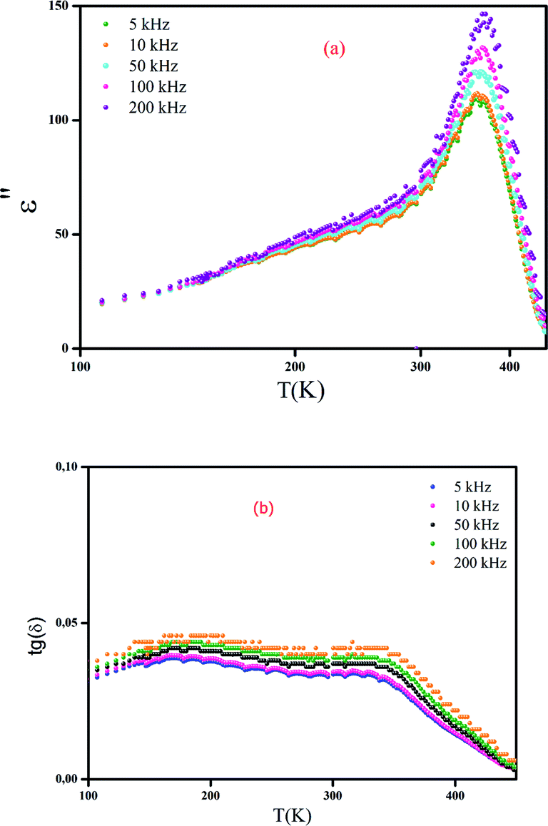 | ||
| Fig. 5 Thermal evolution of the imaginary part of the permittivity (a) and dielectric loss (b) for (Ba0.95Ca0.05)1−xNax(Ti0.8Sn0.2)1−xNbxO3 ceramics with x = 0.85. | ||
Moreover, for a normal ferroelectric, the thermal evolution of dielectric constant above the Curie temperature in the paraelectric region is described by a Curie–Weiss law equation:
 | (2) |
Fig. 6a and b, disclose as an example the thermal evolution of the inverse of  at 10 kHz for x = 0.75 (relaxor) and 0.85 (classical), respectively. The fits to the experimental data are obtained by eqn (2). The relaxor ceramics x = 0.75,
  presents a deviation from the Curie–Weiss law at a deviation temperature Tdev that is defined as the temperature from which it starts to deviate from the Curie–Weiss law. However, the evolution of the inverse of constant dielectric for x = 0.85 obeys the Curie Weiss law implying that the transition from the paraelectric phase to the ferroelectric phase is clearly of the second order and the ferro-electricity is of classical type.38
 | ||
| Fig. 6 Variation of the inverse of the real part of the dielectrique permittivity versus temperature for BCNTSN: (a) x = 0.75 and (b) x = 0.85 ceramics. | ||
Modified Curie law by Uchino and Nomura is used to describe the dielectric relaxation behavior of the (Ba0.95Ca0.05)1−x(Ti0.8Sn0.2)1−xNaxNbxO3 ceramics. Generally, the modified Curie–Weiss law can be described by the following equation described as.39
 | (3) |
 as a function of log(T − Tm) at 10 kHz frequency for the compositions x = 0.75 and x = 0.8 as shown in (Fig. 7a and b). The slope of linear fitting the experimental data to eqn (3) allows determining the values of γ diffusion factor, as listed in Table 3. We observe that the values of γ increase monotonously with the increasing x, indicating a shift toward more diffusive phase transition.41 These results are in good agreement with those reported in the prototype relaxor PbMg1/3Nb2/3O3, 1.6 (ref. 42) and Na1−xSrx(Sn0.25Ti0.75)xNb1−xO3 lead-free43 ceramic.
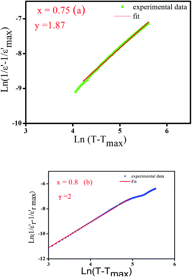 | ||
Fig. 7 Variation of  as a function of ln(T − Tmax) at 10 kHz of (a) x = 0.75 and (b) x = 0.8 of (Ba0.95Ca0.05)1−xNax(Ti0.8Sn0.2)1−xNbxO3 ceramics. as a function of ln(T − Tmax) at 10 kHz of (a) x = 0.75 and (b) x = 0.8 of (Ba0.95Ca0.05)1−xNax(Ti0.8Sn0.2)1−xNbxO3 ceramics. | ||
3.4. Optical properties
The absorbance spectra of all compounds at room temperature in the wavelength range (200–1000 nm) are plotted in Fig. 8. We noticed a decrease of the absorption with the increase of wavelengths whose characteristic peaks are shifted towards smaller wavelengths with the increase in NaNbO3 content, indicating a blue shift, which is suggestive of the increase in the band gap.44 This corresponds to a typical behavior for numerous semiconductors and can refer to many reasons such as internal electric fields within the crystal and inelastic scattering of charge carriers by phonons.45 Furthermore, this behavior may be attributed to the quantum confinement arising from the lowering of particle size.46 | ||
| Fig. 8 Variation of absorbance at room temperature. | ||
These compounds absorb in the UV-visible region with the same order of absorption bands. These bands can be attributed to the inter-band transition which is formed by the 4d orbitals of NbO6 (bottom of conduction band) to 2p orbitals of O2 (top of valence band). The band in the region λ ≥ 400 nm can be associated with an interband transition in relation to the Nb5+ cation.18,47
3.5 Optical band gap and Urbach energies
The optical band gap energy (Eg) values of (Ba0.95Ca0.05)1−xNax(Ti0.8Sn0.2)1−xNbxO3 ceramics are determined using the Kubelka–Munk model as:48
 | (4) |
 | (5) |
The relation used for the determination of the optical band energy is the following:
| αhν = B(hν − Eg)n | (6) |

The value of n depends on the nature of the electronic transition responsible for absorption. It is equal to 1/2 and 3/2 for allowed and forbidden direct transitions respectively and to 2 and 3 for allowed and forbidden indirect transitions respectively.49 Since the perovskite suffers from allowed direct transition, the value of the index n is assumed to be 1/2.25
Fig. 9 highlights the plot of (αhν)2 versus (hν) of all samples. By extrapolating the linear part of the curve to the x-axis; we determine the value of direct band gap energy Eg.
 | ||
| Fig. 9 Plots of (αhν)2 versus photon energy (hν (eV)) for (Ba0.95Ca0.05)1−xNax(Ti0.8Sn0.2)1−xNbxO3 ceramics with x = 0.75, 0.8 and 0.85 compositions. | ||
The calculated values of the optical band gap of the (Ba0.95Ca0.05)1−xNax(Ti0.8Sn0.2)1−xNbxO3 ceramics are found to be 2.89, 2.92 and 3.05 eV for x = 0.75, 0.8 and 0.85, respectively, these values are portrayed in Table 4. Obviously, a little blue shift of the optical band gap occurs when the NaNbO3 content increases, as the pure NN presents a large band gap (Eg = 3.4 eV). This phenomenon may be caused by the Burstein–Moss effect.50 Furthermore, we can notice that the band gap of our ceramics is smaller than that of NaNbO3. This difference can be assigned to the effect of the degree of substitution of the cation Na2+ by (Ba2+, Ca2+) and Nb5+ by (Ti4+, Sn4+) in A and B sites, respectively, which are expected to perturb the electronic structure of the system.
| (Ba0.95Ca0.05Ti0.8Sn0.2)1−xNaxNbxO3 | Eg (eV) | EU (eV) |
|---|---|---|
| 0.75 | 2.89 | 0.348 |
| 0.8 | 2.92 | 0.350 |
| 0.85 | 3.05 | 0.375 |
The narrower band gap might be assigned to an increase in unit cell volume as it can result in a distortion of the unit cell and therefore can produce a decrease in the overlap between O-2p and metal (d) states.51 The forbidden band of ceramics (Ba0.95Ca0.05)1−xNax(Ti0.8Sn0.2)1−xNbxO3 in the order of 3.00 eV, may be useful in photocatalytic and solar cell applications.
The Urbach energy (EU), corresponds to the degree of disorder in the material characterizing the local defects. It can be calculated from the following equation:52
 | (7) |
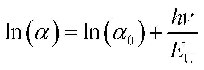 | (8) |
The values of Urbach energy (EU) can be, therefore, obtained from the slope of the straight line of plotting ln(α) against the incident photon energy (hν) Fig. 10. The values of the Urbach energy (EU) of (Ba0.95Ca0.05)1−xNax(Ti0.8Sn0.2)1−xNbxO3 ceramics with x = 0.75, 0.8 and 0.85, are respectively 0.348, 0.350 and 0.375 eV (Table 4). It is worth noting that the Urbach energy increases when the NaNbO3 content increases. As this energy is associated with the microstructural disorder of the network, it can be suggested that the increase in NaNbO3 content leads to an increase in the number of disorders of our ceramics.
 | ||
Fig. 10 Plots of ln![[thin space (1/6-em)]](https://www.rsc.org/images/entities/char_2009.gif) α versus photon energy (hν) of BCNTSNO ceramics with x = 0.75, 0.8 and 0.85 compositions. α versus photon energy (hν) of BCNTSNO ceramics with x = 0.75, 0.8 and 0.85 compositions. | ||
4. Conclusions
Lead free ceramics (Ba0.95Ca0.05)1−x(Ti0.8Sn0.2)1−xNaxNbxO3 (x = 0.75, 0.8 and 0.85), prepared by the conventional solid-solid reaction method, is crystallized in tetragonal structure with space group P4mm. Lattice parameters increase with increasing NaNbO3 concentration. These results can be related to the increase of the ionic radii of the substituted cations.The Raman spectroscopy exhibits a disorder introduced into this composition, which is related to the internal modes of the NbO6 group, and implied that the internal mode was sensitive to the effect of substitution. As a result, this disorder favors a ferroelectric relaxor behavior. The temperature dependence of the dielectric properties of the prepared ceramics reveals that a doping level of Ba, Ca, Sn and Ti modify the NaNbO3 ceramics from antiferroelectric to ferroelectric, implying a decrease in the Curie temperature, with an increase of the dielectric constant. Moreover, the dependence of the dielectric properties on temperature exhibited two behavior a relaxor behavior for the compositions x = 0.75 and 0.8 and a classical ferroelectric behavior for the compositions x = 0.85. The enhancement of the dielectric properties of the NaNbO3 was marked by the shift of the curie temperature to room temperature and the increase of the maxim of permittivity due to (Ba2+, Ca2+) and (Ti4+, Sn4+) substitutions.
Finally, UV-Vis spectra disclose that all lead-free ceramics absorb in the UV-visible region with a blue shift in wavelength along with an increase in NaNbO3 concentration. The Tauc model is used to determine the optical gap energy. The analysis of data indicates the existence of optical indirect gaps, estimated to be in the order of 3 eV, which is much smaller than that NaNbO3 ceramic. Therefore, the improvement of the dielectric and optical properties makes our lead-free ferroelectric material suitable for device memory, in photocatalytic and in solar cell applications.
As perspectives for this work, we can consider making the ferroelectric polarization (P–E) hysteresis and the electrical measurements.
Conflicts of interest
The authors declare that they have no known competing financial interests or personal relationships that could have appeared to influence the work reported in this paper.The authors declare the following financial interests/personal relationships which may be considered as potential competing interests.
References
- Y. Guo, F. Gao, J. Xu, Q. Chen, S. Cao and L. Li, J. Mater. Sci.: Mater. Electron., 2018, 29, 12503–12511 CrossRef CAS.
- L. Zhou, P. Du, Q. Zhang, J. Zhu, Y. Hou, L. Luo and W. Li, J. Alloys Compd., 2019, 810, 151897 CrossRef CAS.
- K. Parida and R. N. P. Choudhary, J. Mater. Sci.: Mater. Electron., 2020, 31, 13292–13300 CrossRef CAS.
- W. Wang, G. Yu, R. Wang and C. Jiang, J. Am. Ceram. Soc., 2020, 103, 432–443 CrossRef CAS.
- Y. Bai, P. Tofel, J. Palosaari, H. Jantunen and J. Juuti, Adv. Mater., 2017, 29, 1700767 CrossRef PubMed.
- Y. Han, X. Ren, Z. Sun, L. Li and S. Yu, J. Mater. Sci.: Mater. Electron., 2019, 30, 15064–15074 CrossRef CAS.
- T. Maeda, N. Takiguchi, M. Ishikawa, T. Hemsel and T. Morita, Mater. Lett., 2010, 64, 125–128 CrossRef CAS.
- Y. Yang, Y. Zhou, J. Ren, Q. Zheng, K. H. Lam and D. Lin, J. Am. Ceram. Soc., 2018, 101, 2594–2605 CrossRef CAS.
- V. V. Atuchin, Nucl. Instrum. Methods Phys. Res., Sect. B, 2000, 168, 498–502 CrossRef CAS.
- R. M. Taziev, IEEE Trans. Sonics Ultrason., 2007, 54(10), 2060–2069 CAS.
- I. Sh. Steinberg, et al., Opt. Mater., 2018, 78, 253–258 CrossRef CAS.
- J. Kreisel, M. Alexe and P. A. Thomas, Nat. Mater., 2012, 11, 260 CrossRef CAS PubMed.
- T. Chen, J. Meng, S. Wu, J. Pei, Q. Lin, X. Wei, J. Li and Z. Zhang, J. Alloys Compd., 2018, 754, 184–189 CrossRef CAS.
- W. Janbua, T. Bongkarn, T. Kolodiazhnyi and N. Vittayakorn, RSC Adv., 2017, 7, 30166–30176 RSC.
- R. Shi, Y. Pu, W. Wang, X. Guo, J. Li, M. Yang and S. Zhou, J. Alloys Compd., 2020, 815, 152356 CrossRef CAS.
- R. Barbosa-Silva, J. F. Silva, U. Rocha, C. Jacinto and C. B. de Araújo, J. Lumin., 2019, 211, 121–126 CrossRef CAS.
- A. M. Hamilton, S. ODonnell, B. Zoellner, I. Sullivan and P. A. Maggard, J. Am. Ceram. Soc, 2019, 103(1), 454–464 CrossRef.
- S. Prasertpalichat and D. P. Cann, J. Electroceram., 2014, 33, 214–220 CrossRef CAS.
- Y.-Q. Xu, S.-Y. Wu, L.-N. Wu, C.-C. Ding and L.-J. Zhang, Int. J. Mod. Phys. B, 2018, 32, 1850282 CrossRef CAS.
- D. Zhang, J. Cheng, F. Shi, Z. Cheng, X. Yang and M. Cao, RSC Adv., 2015, 5, 33001–33007 RSC.
- Q. Liu, L. Zhang, Y. Chai and W.-L. Dai, J. Phys. Chem. C, 2017, 121, 25898–25907 CrossRef CAS.
- S. Khemakhem, S. Yahyaoui, R. Ben Hassen, H. Khemakhem and A. Ben Salah, Solid State Sci., 2003, 5, 367–371 CrossRef CAS.
- Y. D. Juang, S. B. Dai, Y. C. Wang, J. S. Hwang, M. L. Hu and W. S. Tse, J. Appl. Phys., 2000, 88, 742–745 CrossRef CAS.
- H. Khelifi, A. Aydi, N. Abdelmoula, A. Simon, A. Maalej, H. Khemakhem and M. Maglione, J. Mater. Sci., 2012, 47, 1943–1949 CrossRef CAS.
- S. K. Mohanty, H. S. Mohanty, B. Behera, D. P. Datta, S. Behera and P. R. Das, J. Mater. Sci.: Mater. Electron., 2019, 30, 5833–5844 CrossRef CAS.
- X. B. Wang, Z. X. Shen, Z. P. Hu, L. Qin, S. H. Tang and M. H. Kuok, J. Mol. Struct., 1996, 385, 1–6 CrossRef CAS.
- N. Baskaran and H. Chang, Mater. Chem. Phys., 2003, 77, 889–894 CrossRef CAS.
- H. M. Rietveld, J. Appl. Crystallogr., 1969, 2, 65–71 CrossRef CAS.
- W. Beskow and V. M. Goldschmidt, Geologiska Föreningen i Stockholm Förhandlingar, 1924, 46(6–7), 738–743 CrossRef.
- A. Bauzá, T. J. Mooibroek and A. Frontera, CrystEngComm, 2016, 18, 10–23 RSC.
- H. Slimi, A. Oueslati and A. Aydi, Appl. Phys. A, 2019, 510, 1–10 Search PubMed.
- M. Boukriba, F. Sediri and N. Gharbi, Mater. Res. Bull., 2013, 48, 574–580 CrossRef CAS.
- I. Zouari, Z. Sassi, L. Seveyrat, V. Perrin, S. Zghal, N. Abdelmoula, L. Lebrun and H. Khemakhem, J. Electron. Mater., 2017, 46, 4662–4669 CrossRef CAS.
- F. Kang, L. Zhang, B. Huang, P. Mao, Z. Wang, Q. Sun, J. Wang and D. Hu, J. Eur. Ceram. Soc., 2020, 40, 1198–1204 CrossRef CAS.
- A. Simon, J. Ravez and M. Maglione, J. Phys.: Condens. Matter, 2004, 16, 963–970 CrossRef CAS.
- Y. Han, X. Ren, Z. Sun, L. Li and S. Yu, J. Mater. Sci.: Mater. Electron., 2019, 30, 15064–15074 CrossRef CAS.
- R. Roukos, J. Romanos, S. A. Dargham and D. Chaumont, J. Eur. Ceram. Soc., 2019, 39, 2297–2303 CrossRef CAS.
- J. Ma, X. Liu, C. Zhou, C. Yuan, W. Li and M. Jiang, Ceram. Int., 2014, 40, 2979–2984 CrossRef CAS.
- K. Uchino and S. Nomura, Ferroelectrics, 1982, 44, 55–61 CrossRef CAS.
- Z. Raddaoui, S. El Kossi, J. Dhahri, N. Abdelmoula and K. Taibi, RSC Adv., 2019, 9, 2412–2425 RSC.
- J. Hao, Z. Xu, R. Chu, W. Li, G. Li and Q. Yin, J. Alloys Compd., 2009, 484, 233–238 CrossRef CAS.
- K. Hao, W. Ge, Z. Ren, X. Liu, L. Luo, X. Li, H. Luo and D. Viehland, J. Am. Ceram. Soc., 2020, 103, 3349–3360 CrossRef CAS.
- S. Aydi, A. Amouri, S. Chkoundali and A. Aydi, Ceram. Int., 2017, 43, 12179–12185 CrossRef CAS.
- S. Li, Y.-H. Lin, B.-P. Zhang, Y. Wang and C.-W. Nan, J. Phys. Chem. C, 2010, 114, 2903–2908 CrossRef CAS.
- W. Ben Nasr, A. Mahmoud, F. Boschini and A. Ben Rhaiem, J. Alloys Compd., 2019, 788, 522–532 CrossRef CAS.
- A. K. Sinha, B. Bhushan, J. Jagannath, R. K. Sharma, S. Sen, B. P. Mandal, S. S. Meena, P. Bhatt, C. L. Prajapat, A. Priyam, S. K. Mishra and S. C. Gadkari, Results Phys., 2019, 13, 102299 CrossRef.
- Z. Wang, H. Gu, Y. Hu, K. Yang, M. Hu, D. Zhou and J. Guan, CrystEngComm, 2010, 12, 3157 RSC.
- S. A. Ansari, A. Nisar, B. Fatma, W. Khan and A. H. Naqvi, Mater. Sci. Eng., B, 2012, 177, 428–435 CrossRef CAS.
- R. Jeevan Kumar and D. Kothandan, Int. J. ChemTech Res., 2015, 8, 410–314 Search PubMed.
- V. Kumar and S. Singh, J. Alloys Compd., 2018, 732, 350–357 CrossRef CAS.
- B. Bhushan, A. Basumallick, N. Y. Vasanthacharya, S. Kumar and D. Das, Solid State Sci., 2010, 12, 1063–1069 CrossRef CAS.
- R. Lefi, F. Ben Naser and H. Guermazi, J. Alloys Compd., 2017, 696, 1244–1254 CrossRef CAS.
| This journal is © The Royal Society of Chemistry 2021 |