
 Open Access Article
 This Open Access Article is licensed under a Creative Commons Attribution-Non Commercial 3.0 Unported Licence
High-performance broadband photodetectors based on all-inorganic perovskite CsPb(Br/I)3 nanocrystal/CdS-microwire heterostructures†
Haixia Li *,
Weiwei Lin,
Liang Ma,
Yang Liu,
Yu Wang,
Ao Li,
Xiaorui Jin and
Lun Xiong*
*,
Weiwei Lin,
Liang Ma,
Yang Liu,
Yu Wang,
Ao Li,
Xiaorui Jin and
Lun Xiong*
Hubei Key Laboratory of Optical Information and Pattern Recognition, School of Optical Information and Energy Engineering, School of Mathematics and Physics, Wuhan Institute of Technology, Guanggu 1st Road 206, Wuhan 430205, P. R. China. E-mail: lihaixia@wit.edu.cn; xionglun@wit.edu.cn
First published on 22nd March 2021
Abstract
High-performance broadband photodetectors that can operate at UV, visible, and near-infrared wavelengths have been fabricated based on CsPb(Br/I)3 nanocrystal (NC)/CdS-microwire (MW) heterostructures. Under an incident light illumination of 365, 530, and 660 nm, the CsPb(Br/I)3-NC/CdS-MW-heterostructure-based photodetector exhibited a superior photosensitivity and broader spectral response than those of a bare-CdS-MW-based photodetector, which can be attributed to the light-trapping ability of the CsPb(Br/I)3 NCs and charge-transfer efficiency at the CsPb(Br/I)3-NC/CdS-MW-heterojunction interface. The photodetector based on the CsPb(Br/I)3 NC/CdS-MW heterostructure also exhibited a good response to near-infrared light (760 and 810 nm) because the produced heterojunction facilitates the spatial separation of the photogenerated carriers, and the carriers are transferred from the CsPb(Br/I)3 NC part to the CdS MW part through diffusion due to the relatively long diffusion length in the CsPb(Br/I)3 layer. Therefore, the proposed photodetectors are promising for constructing high-performance broadband optoelectronic devices.
1. Introduction
Semiconductors of groups II–VI, especially CdS, have attracted great research interest due to their direct wide band gap (2.4 eV), good optical properties, and environmental stability. These properties render them suitable for developing high-performance photodetectors, field-effect transistors, light-emitting diodes, and batteries.1–6 Photodetectors are of great importance because of their excellent performance and wide application in photoswitching, photoelectric conversion, and optical communication.7–11 Several groups have proposed photodetectors fabricated using different CdS nanostructures.12–14 Although this is considered a breakthrough in the field, these photodetectors exhibit relatively restricted performance due to the limited optoelectronic-transfer efficiency and light-absorption ability of the CdS nanomaterials. In addition, owing to the intrinsic electronic band structure of the material itself, the spectral selectivity of the current photodetectors is limited to a wavelength range of 300–520 nm. For example, a photodetector based on a CdS:Ga nanoribbon/Au Schottky junction exhibited rise/fall times of 95/290 ms, respectively. However, due to the large band gap of CdS nanoribbons, this device could only detect illumination at a wavelength shorter than 510 nm.15A broadband response photodetector enables light detection in multiple wavelength ranges, which allows a single device to perform several tasks previously achieved by multiple devices. Thus, in recent years, broadband response photodetectors have received significant research interest. However, the research on broadband photodetectors that can respond to light at different wavelengths is still lacking.
To overcome these problems, several strategies, such as integration with strong light-absorbing materials to form heterojunctions16 and novel architecture design,17 have been proposed. The all-inorganic cesium-lead halide (CsPbX3, X = Cl, Br, I, or mixed Cl/Br and Br/I) perovskite nanocrystals (NCs) have been proposed as a strong light-absorbing material for several applications, such as solar cells,18 light-emitting diodes,19,20 and photodetectors.21–23 These materials offer several advantages, such as strong light-absorbing property, long diffusion length of the charge carriers, and low-cost solution processing.24–26 In addition, it is possible to tailor the band gap of the CsPbX3 materials by changing the halide or through anion-exchange reactions.27 CsPbX3 NCs can be excited by high-energy photons (wavelength < 400 nm), but they are more sensitive to the whole-visible-light window (wavelength: 408–694 nm), which renders them ideal sensitizers for combining with other light-sensitive materials to form heterojunction and improve the photoresponse.28 For optical materials, depending on the nature of the heterocombinations, these could help in either confining or efficiently transporting the photogenerated carriers from one counterpart to another. Thus, depending on the coupled materials, heterostructures composed of two materials exhibit better optical stability than single materials.29–31
Excellent results have been obtained using these heterostructures. You et al. reported a photodetector based on a CsPbBr3/ZnO heterostructure using solution processing.32 Owing to the interfacial charge transfer from perovskite to ZnO, the light photocurrent of the devices was enhanced by more than one order of magnitude. In addition, the photodetector exhibited a broader photoresponse range up to 450 nm owing to the high-absorption coefficient and large spectral coverage of the CsPbBr3/ZnO heterostructure. However, the spectral response range of the detector cannot cover the whole ultraviolet and visible region; thus, the broadband photodetectors still require wider investigation. The band-gap energies of CsPb(Br/I)3 NCs and CdS nanomaterials are approximately 1.9 and 2.4 eV, respectively, which makes them ideal for band alignment.17,19 Thus, the authors believe that CsPb(Br/I)3 NCs/CdS microwires (MWs) heterostructures are promising candidates for the fabrication of high-performance broadband photodetectors.
In this study, a high-performance broadband photodetector based on CsPb(Br/I)3 NC/CdS-MW heterostructures was fabricated using a convenient method. The photodetector performance was systematically investigated in terms of current responsivity (R), external quantum efficiency (EQE), detectivity (D*) at 365, 530, 660, 760, and 810 nm. The device exhibited broadband photodetection that covers the UV-visible-near-infrared (UV-VIS-NIR) range (up to 810 nm) and a superior photosensitivity, which is attributed to the charge transfer at the interface and the absorption capability of CsPb(Br/I)3 NCs.
2. Experimental section
2.1 Growth of CdS MWs
The CdS MWs were synthesized following a method described in a previous study.17 The CdS MWs were grown on an Si substrate using chemical vapor deposition (CVD) in a horizontal tube furnace. First, a mixture (1 g) of CdS (99.99%) and bismuth (99.999%) powders were placed at the center of a quartz boat. Next, the boat was transferred into the center of the quartz tube, and the Si substrate was placed at a 16 cm distance from the source to collect the deposited products. Ar (100 sccm) was used as the carrier gas during the MW growth. The furnace was heated to 950 °C over 45 min and maintained at this temperature for another 45 min. The furnace was then naturally cooled to room temperature (RT), and the wool-like light-yellow products were collected.2.2 Synthesis of CsPb(Br/I)3 NCs
CsPb(Br/I)3 NCs were synthesized by first mixing cesium carbonate (Cs2CO3, 0.4 g), oleic acid (OA, 2 ml), and 1-octadecene (ODE, 20 ml) in a 50 ml three-necked flask and dried at 120 °C for 1 h. Next, the mixture was heated to 120 °C under N2 atmosphere to completely dissolve the Cs2CO3 powder. The produced Cs-oleate solution was then stored at RT and preheated to 100 °C immediately before using it in the synthesis of CsPb(Br/I)3 NCs.Following a typical synthesis of CsPb(Br/I)3 NCs, PbBr2 (0.047 mmol), PbI2 (0.141 mmol), and ODE (5 ml) were loaded into a 50 ml three-necked flask and dried under vacuum at 120 °C for 1 h. Dried OA (0.5 ml) and oxalic acid monothioester (OAm, 0.5 ml) were injected under N2 flow at 120 °C. The temperature was then increased to 160 °C, at which the Cs-oleate (0.4 ml) was rapidly injected. After 5 s, the reaction mixture was cooled down to RT by immersion in a cold-water bath. The NCs were precipitated out of crude solutions at RT and separated by centrifugation at 12![[thin space (1/6-em)]](https://www.rsc.org/images/entities/char_2009.gif) 000 rpm for 10 min. The precipitates were dissolved in hexane, and ethyl acetate was added to the hexane dispersion and centrifuged at 10000 rpm for 5 min. After decanting the supernatant, the final precipitates were redispersed in hexane for further use.
000 rpm for 10 min. The precipitates were dissolved in hexane, and ethyl acetate was added to the hexane dispersion and centrifuged at 10000 rpm for 5 min. After decanting the supernatant, the final precipitates were redispersed in hexane for further use.
2.3 Photodetector fabrication
After the CdS MWs growth, an ultralong (∼0.1 cm) CdS MW was deposited on the polyethylene terephthalate (PET) substrate. Then after, the silver paste was applied at the both ends of the single CdS MW. The sample was then dried in a furnace at 150 °C for 1 h under an air atmosphere, and the resulting silver paste was used to fabricate the electrodes. Photodetectors with two-terminal structures were fabricated using single CdS MWs to form the working element. Next, the CsPb(Br/I)3-NC/CdS-MW-heterostructure photodetector was built through a crystallization process on individual CdS-MW devices. In this process, a small amount of CsPb(Br/I)3 NC precursor solution was spin-coated (3000 rpm) on the as-fabricated CdS MWs photodetectors, and the sample was then heated under an air atmosphere at 80 °C (on a hot plate) for 0.5 h, which resulted in a CdS MW with its entire surface uniformly covered with colloidal CsPb(Br/I)3 NCs.2.4 Measurements
The morphology and crystalline structure of the as-deposited CdS MWs and CsPb(Br/I)3 NCs were characterized using field-emission scanning electron microscopy (FSEM: FEI Nova Nano-SEM 450) and high-resolution transmission electron microscopy (HRTEM: FEI Titan G2 60-300), X-ray diffraction (X'pert Pro, PANalytical B.V., Netherlands). The photoluminescence (PL) tests of the single CdS MW and CsPb(Br/I)3 NCs were performed at RT using an He–Cd laser (λ = 325 and 532 nm). The extinction spectra were analyzed using UV-VIS-NIR spectrophotometry (TU1810, Beijing Pgeneral). All measurements were carried out at RT under ambient conditions. An ultraviolet photoelectron spectroscopy (UPS, AXIS-ULTRA DLD-600W) was employed for the work function measurement. The UV-NIR photoresponse was measured between two electrodes at a fixed bias voltage of 5 V by changing the wavelength of a portable lamp light (λ = 365, 530, 660, 760, and 810 nm).3. Results and discussion
Fig. 1(a) shows the structural representation of the photodetector based on CsPb(Br/I)3 NC/CdS-MW heterostructures. The silver paste bonded to the two materials used as electrodes. Fig. 1(b) represents the as-fabricated photodetectors based on CsPb(Br/I)3-NC/CdS-MW-heterostructure, and the entire surface of the CdS MW was uniformly covered with CsPb(Br/I)3 NCs. The energy-band-structure diagram of the CsPb(Br/I)3 NC/CdS-MW heterostructures (Fig. 1(c)) indicates the energy difference in the conduction band minimum between CsPb(Br/I)3 NCs and CdS MW, resulting in the formation of a depletion region, which facilitates the separation of the photogenerated electron–hole pairs in the perovskite layer and electron transfer across the interface of the heterojunction. Under constant external operating conditions, the response performance of the photodetectors was largely determined by the absorption capability of the CsPb(Br/I)3 NC layer and the charge-transfer efficiency at the interface between CsPb(Br/I)3 NCs and CdS-MW heterostructures. As mentioned above, the combination of CsPb(Br/I)3 NCs and CdS MWs may offer new possibilities for fabricating photodetectors with high performances due to the strong absorption capability and matching band structure of the two materials.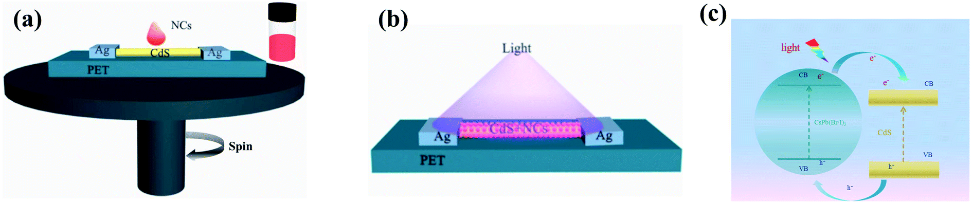 | ||
| Fig. 1 Schematics illustrating the working mechanism of CsPb(Br/I)3-NC/CdS-MW-heterostructure photodetector: (a) the photodetector based on CsPb(Br/I)3 NC/CdS-MW heterostructures, which consists of a PET substrate and a silver paste contacts, (b) a photodetector based on CsPb(Br/I)3 NC/CdS-MW heterostructures under illumination, and (c) a simplified energy-band alignment of the photodetectors showing the charge transfer at the interface of CsPb(Br/I)3 NC/CdS-MW heterostructures under a laser light. | ||
Fig. 2(a) shows a typical SEM image of CdS MWs, which indicates that the diameters of MWs ranged from several hundred nanometers to several micrometers. Fig. 2(b) shows a TEM image of CsPb(Br/I)3 NC/CdS-MW heterostructures, which shows that CsPb(Br/I)3 NCs were uniformly distributed on the surface of the CdS-MW wire. Fig. 2(c) shows the HRTEM image of high-quality CdS MWs decorated with CsPb(Br/I)3 NCs. The lattice spacing within the bulk of the CsPb(Br/I)3 NC/CdS-MW-hybrid structures was measured to be approximately 0.334 nm, indicating that the as-prepared CdS was a single crystal with a preferred growth direction parallel to the [001] direction.12 The HRTEM image recorded within the decoration layer shows that the CsPb(Br/I)3 NCs exhibited a cubic structure with the range of 10–20 nm. The HRTEM image also indicates that CsPb(Br/I)3 NCs had a well-defined crystalline structure with a cubic lattice parameter of 0.296 nm along the [210] direction.19 The energy-dispersive X-ray (EDX) spectroscopy mapping (Fig. 2(d)) revealed a homogeneous spatial distribution of Cd and S within the CdS-MW part, while the signals from element Cs, Pb, Br, and I were obtained from the entire coated area of the CsPb(Br/I)3 NC/CdS-MW hybrid-structure. As shown in Fig. S1,† energy-dispersive spectroscopy (EDS) analysis was used to assess the chemical composition of the fabricated CsPb(Br/I)3 NC/CdS-MW heterostructure. It indicated that the hybrid structures contained elemental Cd, S, Cs, Pb, I, and Br. As mentioned above, these results indicate that the CsPb(Br/I)3 NCs were wrapped around MWs.
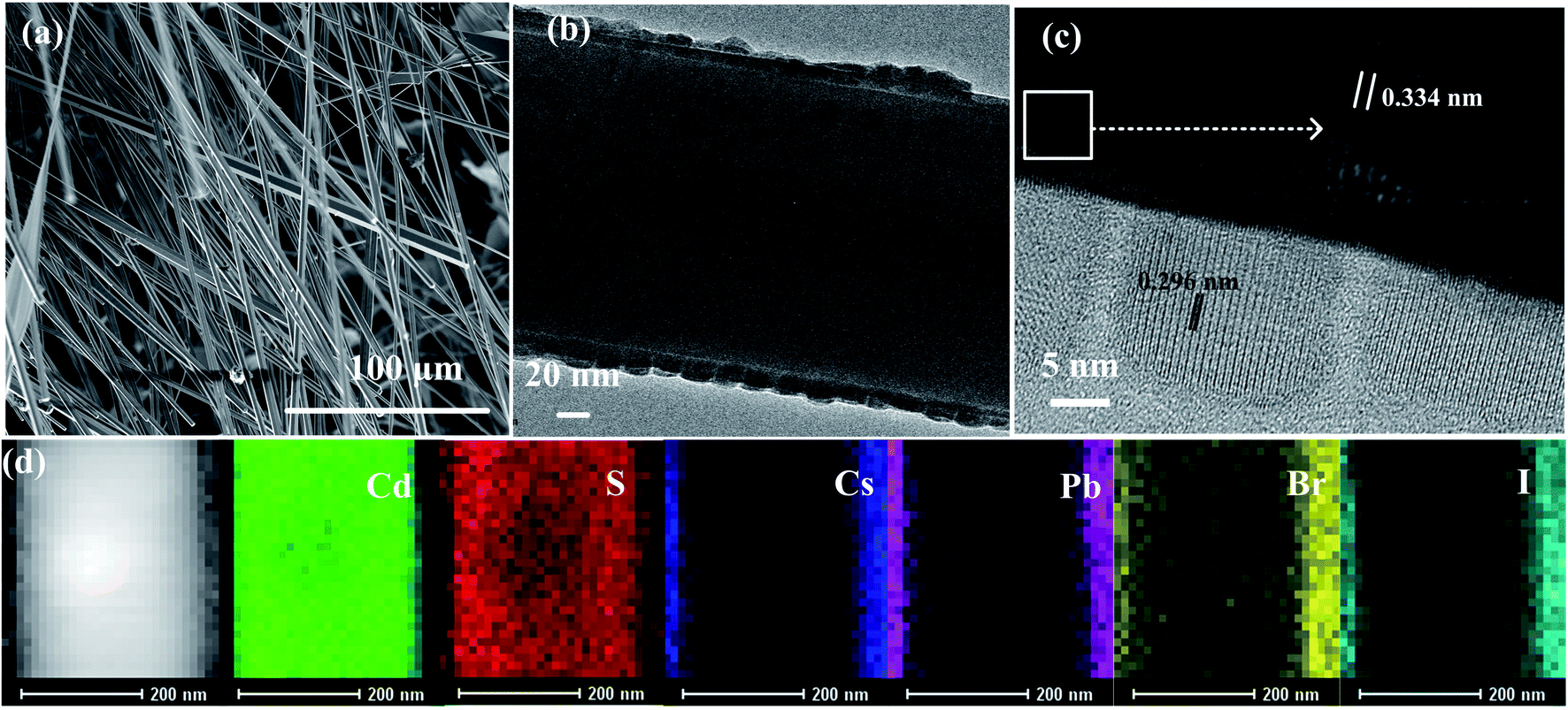 | ||
| Fig. 2 Characterization of CdS MWs and CsPbBr3 NCs: (a) a typical enlarged SEM image of CdS MWs, (b) a typical TEM image of CdS MWs, (c) a typical HRTEM image of CsPb(Br/I)3 NC/CdS-MW heterostructures, and (d) elemental mappings of CsPb(Br/I)3 NC/CdS-MW heterostructures of the selected area. | ||
Fig. 3(a and b) show the XRD patterns of as-fabricated CdS MWs and CsPb(Br/I)3 NCs, respectively. These tests were performed to explore the phase structure of CdS MWs and CsPb(Br/I)3 NCs. For the Fig. 3(a), all the diffraction peaks can be assigned to CdS MWs with a hexagonal wurtzite structure, which indicates the good crystallinity of CdS MWs and agrees with the standard date file (JCPDS no. 41-1049).17 Fig. 3(b) shows the XRD result of the CsPb(Br/I)3 NCs (JCPDS no. 54-0752);19 two additional diffraction peaks appeared at 15.2° and 30.6° that can be assigned to (100) and (200), respectively, which correspond to the cube morphology indicated by Fig. 1(c). Compared to the CsPbBr3 NC peaks, those of CsPb(Br/I)3 NCs were shifted to a lower angle (the lower part of Fig. 3(b)). This deviation could be attributed to the atomic radius of I, which is larger than that of Br, leading to an extended lattice.32
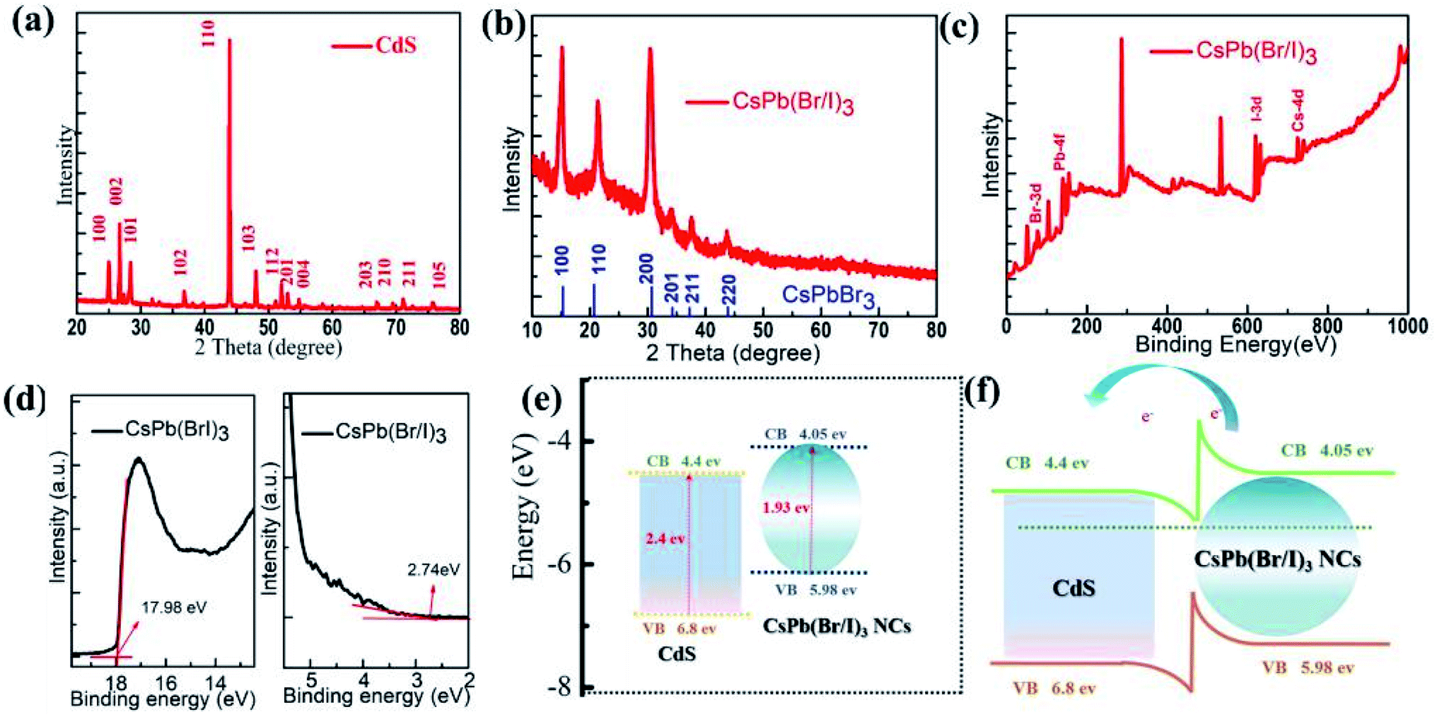 | ||
| Fig. 3 (a) The XRD profile of the as-fabricated CdS MWs with a PDF card no. 41-1049, (b) the XRD profile of the CsPb(Br/I)3 NCs with PDF card no. 54-0752, (c) XPS spectra of the CsPb(Br/I)3 NCs, (d) the left panel shows the UPS spectra of CsPb(Br/I)3 NCs from 19 to 13.5 eV. The right panel shows the UPS spectra illustrating the magnified view of the low binding-energy region of CsPb(Br/I)3 NCs, (e) the energy-level diagrams of CsPb(Br/I)3 NCs and CdS MWs before contact, and (f) a band diagram of the CsPb(Br/I)3 NC/CdS-MW heterostructures under equilibrium in the dark. | ||
X-ray photoelectron spectroscopy (XPS) studies were conducted to further investigate the elemental composition of CsPb(Br/I)3 NCs. The results (Fig. 3(c)) indicated the presence of Cs, Pb, Br, and I in CsPb(Br/I)3 NCs. Fig. S2 (ESI†) shows that the high-resolution XPS spectra of Cs-3d, Pb-4f, Br-3d, and I-3d in CsPb(Br/I)3 NCs were observed at 725.55, 136.15, 69.90, and 619.95 eV, respectively, which are similar to results of previous reports.19
Fig. 3(d) shows the UPS results of CsPb(Br/I)3 NCs. The energy at the top of the valence band was calculated based on the lowest binding energy. In addition, the work function of CsPb(Br/I)3 NCs was calculated to be 3.24 eV by subtracting the secondary electron cut-off energy of CsPb(Br/I)3 NCs (17.98 eV) from the incident ultraviolet photon energy (21.22 eV).33 Moreover, the energy difference between the Fermi level (EF) and the top of the CsPb(Br/I)3 NC valence band was determined to be 2.74 eV. Based on the bandgaps in CsPb(Br/I)3 NCs (1.93 eV), the valence band maximum (VBM) and the conduction band minimum (CBM) values of CsPb(Br/I)3 were determined to be −5.98 and −4.05 eV, respectively. According to the literature, the VBM and CBM of CdS are approximately −6.8 and −4.4 eV, respectively.34 Fig. 3(e) shows the energy-level alignment of the CsPb(Br/I)3 NCs/CdS MWs. Fig. 3(f) illustrates the energy-level diagrams of CsPb(Br/I)3 NC/CdS-MW-hybrid structures under equilibrium in the dark. The electrical junction was formed when the CsPb(Br/I)3 NCs were brought into contact with CdS MWs, and that electrons diffused from CsPb(Br/I)3 NCs to CdS MWs to align the Fermi levels of the materials and reach a new equilibrium. This charge transfer caused the energy band to bend, resulting in the formation of a depletion region and a built-in field. As a result of the incident laser excitation, the electron–hole pairs were mainly generated in the highly light-absorbing CsPb(Br/I)3 NC layer and then separated by the built-in field. This was followed by the diffusion of the electrons and holes to the CdS-MW and CsPb(Br/I)3 NC sides, respectively. This optimal energy-level alignment is the reason for the transfer of a great part of the photogenerated carriers from the CsPb(Br/I)3 NC part to the CdS part through diffusion, due to the relatively long diffusion length in the CsPb(Br/I)3 NC layer. Thus, a good charge-carrier transport can be obtained, which improves the photoresponsivity.
The optical properties of CdS MWs, CsPb(Br/I)3 NCs, and the CsPb(Br/I)3 NC/CdS-MW-hybrid structures were examined using UV-vis spectroscopy (Fig. 4(a), the inset is the optical images of the colloidal solutions of CsPb(Br/I)3 NCs under UV illumination). CdS MWs and CsPb(Br/I)3 NCs show absorption edges at approximately 542 and 640 nm, respectively, which were close to the near-band-edge emission of 2.40 and 1.93 eV in the PL spectra (Fig. 4(b)). On the other hand, the CsPb(Br/I)3 NC/CdS-MW heterostructures showed enhanced absorption below a wavelength of 640 nm, which can be attributed to the synergetic absorption effect of CsPb(Br/I)3 NCs and CdS MWs. This improvement in the light absorption in the heterostructures can enhance the photodetector performance, including photosensitivity and detectivity.
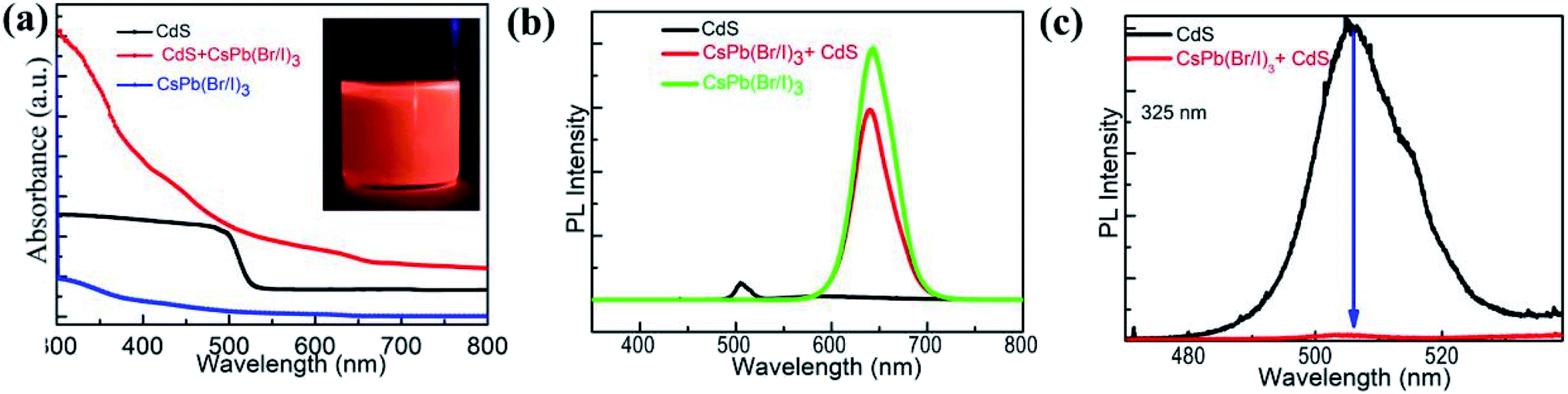 | ||
| Fig. 4 (a) UV-vis absorption spectra of CsPb(Br/I)3 NCs, CdS MWs, and the CsPb(Br/I)3 NC/CdS MW heterostructures; inset is the optical images of the colloidal solutions of CsPb(Br/I)3 NCs under UV illumination. (b) PL spectra of CsPb(Br/I)3 NCs, CdS MWs, and the CsPb(Br/I)3 NC/CdS MW heterostructures under an excitation wavelength of 325 nm. (c) Magnified view of the PL spectra of CdS MWs and the CsPb(Br/I)3 NC/CdS MW heterostructures. | ||
Fig. 4(b) illustrates the PL spectra of CdS MWs, CsPb(Br/I)3 NCs, and the CsPb(Br/I)3 NC/CdS-MW heterostructures upon excitation at 325 nm. Fig. S3† shows the individual spectra of CdS MWs, CsPb(Br/I)3 NCs, and CsPb(Br/I)3 NC/CdS MW heterostructures. The black line in Fig. 4(b) shows that only a strong green emission at approximately 517 nm (2.4 eV) was detected, which indicates good crystallinity and low-defect concentration of the fabricated CdS MWs. Consequently, the fabricated CdS MWs were investigated for their photodetection performance. In case of CsPb(Br/I)3 NCs (green line), the PL emission spectrum shows a peak position at 640 nm, revealing that the band-gap energy between the conduction-band and valence-band edges of CsPb(Br/I)3 NCs was ∼1.93 eV, which is consistent with the results of UV-vis and with those of the CsPb(Br/I)3 quantum-dots previously reported.35 In case of the CsPb(Br/I)3 NC/CdS-MW heterostructures (red line), two PL peaks were observed at 517 and 636 nm. In comparison to the CsPb(Br/I)3 NCs-only PL spectrum, a significant decrease in the band-to-band transition peak was clearly detected in the CsPb(Br/I)3 NC/CdS-MW heterostructures. The PL intensity is mainly determined by dipole–dipole couplings or charge transfer. The dipole–dipole interaction arising from dipole moments between acceptors and donors typically occurs among molecules.36,37 In the charge-transfer mechanism, the nonradiative rate of two adjacent photosensitive materials can be simultaneously increased because of the light-emission quenching from all transitions.38 This proves that a large part of the photogenerated carriers may be transferred from the CsPb(Br/I)3 NC part to the CdS part through diffusion due to the relatively long diffusion length in CsPb(Br/I)3 layer. Thus, this good charge-carrier transport would enhance the photoresponsivity,16 which indicates that the fabricated CsPb(Br/I)3 NC/CdS MW-hybrid materials are suitable for photodetection investigation.
Fig. 5(a, d, g) show the current–voltage (I–V) characteristics measured in darkness and under a constant illumination of 365 (2.22 mW cm−2), 530 (1.66 mW cm−2), and 660 nm (2.61 mW cm−2), respectively. The figures show that the photocurrent increased with the light-irradiation intensity. Fig. 5(b, e, h) show the on–off current response of the photodetector under the three light-illumination intensities at a bias voltage of 5 V. The photocurrent increased with the intensity of the light illumination and exhibited no saturation. In case of the CsPb(Br/I)3-NC/CdS-MW-heterostructure-based photodetector, which decreased the rise and decay times (rise time < 0.1 s, decay time < 0.1 s) compared to bare-CdS-MW-based photodetectors (rise time ≈ 0.2 s, decay time ≈ 0.2 s) (Fig. 5(c, f, i)). The on–off current ratio of the CsPb(Br/I)3-NC/CdS-MW-heterostructures-based photodetector, which is defined as  , was calculated to be 3.93 × 10³, 1.9 × 10³, and 1.1 × 10³ under the 365, 530, and 660 nm illuminations, respectively, which is much higher than the photodetectors based on bare-CdS-MWs.
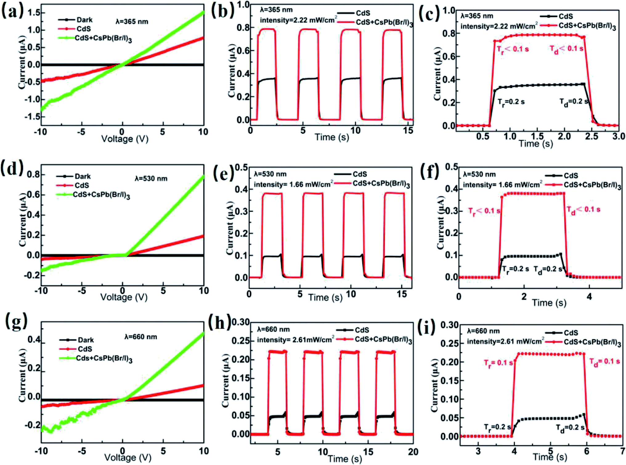 | ||
| Fig. 5 The I–V characteristics measured in darkness and under a constant illumination of (a) 365 nm (2.22 mW cm−2), (d) 530 nm (1.66 mW cm−2), and (g) 660 nm (2.61 mW cm−2). The time-response behaviors recorded under (b) 365 nm, (e) 530 nm, and (h) 660 nm. The rise and fall times in the photocurrent extracted from (c) panel (b), (f) panel (e), and (i) panel (h). | ||
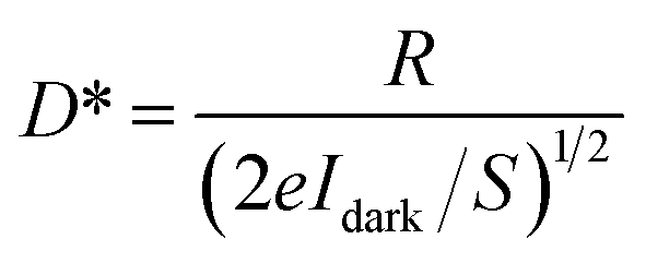
To further evaluate the performance of the photodetectors, critical parameters such as detector current responsivity (R), external quantum efficiency (EQE), and detectivity (D*) were calculated using the following formulas:
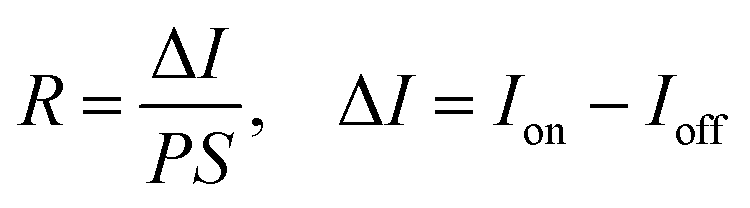
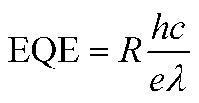
where Ioff is the current measured in darkness, Ion is the photocurrent, S is the activity zone under incident light, h is Plank's constant, and e is the electron charge.39,40 Tables S1–S3 (ESI†) summarize these parameters (R, EQE, D*) for the CsPb(Br/I)3-NC/CdS-MW- and CdS-MW-based photodetectors under illumination of 365, 530, and 660 nm (the applied bias = 5 V). The photodetectors based on CsPb(Br/I)3 NC/CdS-MW heterostructures were found to have high photosensitivity compared to the bare-CdS-MW-based photodetectors.
This remarkable enhancement can be attributed to the photodetector structure and band alignment at the interface of CdS MW and CsPb(Br/I)3 NC heterostructures (Fig. 3(f)). When CsPb(Br/I)3 NCs are placed on the surface of CdS MWs, a type-II heterojunction is produced and the energy difference in the conduction band minimum between CsPb(Br/I)3 NCs and CdS MW resulting in the formation of a depletion region, which facilitates the spatial separation of the photogenerated carriers and reduces the recombination rate of the electron–hole pairs. Therefore, the response time of the photodetectors was shortened by the charge-transfer efficiency at the interface between CsPb(Br/I)3 NCs and CdS-MW heterostructures. A similar improvement has been reported in preciously developed heterojunction.26 Moreover, as mentioned earlier in Fig. 4(b), the PL peaks of CsPb(Br/I)3 NC/CdS-MW heterostructures (red line) revealed a significant decrease in the band-to-band transition peak compared to that in the CsPb(Br/I)3-only PL spectrum, which indicates that a great proportion of the photogenerated carriers may be transferred from the CsPb(Br/I)3 NC part to the CdS MWs part through diffusion due to the relatively long diffusion length and the superior absorption capability of the CsPb(Br/I)3 layer. This good charge-carrier transport enhances the photoresponsivity of the CsPb(Br/I)3-NC/CdS-MW-heterostructures-based photodetectors. In addition, oxygen adsorption and desorption at the surface defect sites is believed to play a critical role in the response time of CdS MWs. In this case, as the CdS MWs were decorated with the CsPb(Br/I)3 NCs, which may prevent or reduce the carrier recombination at the surface of CdS MWs as a result of oxygen adsorption and desorption, the influence of oxygen molecules on the photoresponse was weakened.17 Therefore, the CsPb(Br/I)3-NC/CdS-MW-heterostructures-based photodetectors exhibit fast dynamic changes and shorter rise/fall times compared to bare-CdS MWs.
In addition to the excellent photodetection in UV light, green light, and red light, the CsPb(Br/I)3 NC/CdS-MW heterostructures photodetector exhibited a good response to near-infrared light at constant light intensity (760 nm, 3.45 mW cm−2; 810 nm, 5.45 mW cm−2). Tables S4 and S5 (ESI†) summarize these parameters (R, EQE, D*) for the CsPb(Br/I)3-NC/CdS-MW- and CdS-MW-based photodetectors under the illuminations of 760 and 810 nm (applied bias = 5 V). Fig. 6 illustrates the I–V characteristics and photocurrent plot over time. The results shows a similar behavior of the heterostructures to that observed under UV and visible-light irradiations. However, the photocurrent under near-infrared illumination was much smaller than that under UV and visible lights, which is mainly due to the near absence of direct band-to-band absorption that causes a low absorption efficiency in CdS and CsPb(Br/I)3 NCs at longer wavelengths.
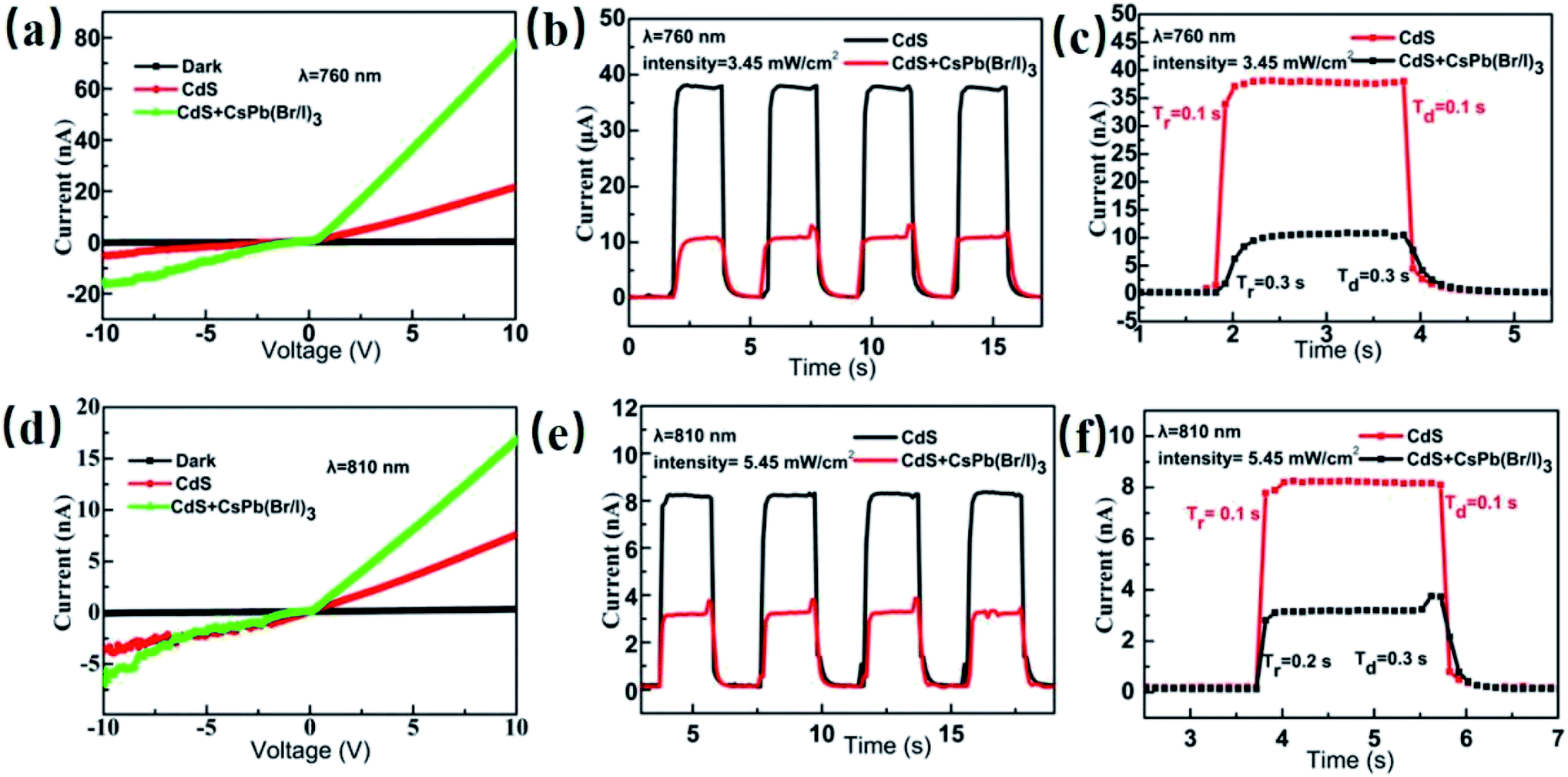 | ||
| Fig. 6 The I–V characteristics measured in darkness and under a constant illumination of (a) 760 nm (3.45 mW cm−2) and (d) 810 nm (5.45 mW cm−2). The time-response behaviors recorded under (b) 760 nm and (e) 810 nm. The rise and fall times of the photocurrent extracted from (c) panel (b) and (f) panel (e). | ||
The photon energies at the near-infrared wavelengths were compared to the band gaps of CsPb(Br/I)3 NCs and CdS MWs. The results showed that the energy of the near-infrared photons was not sufficient to cause direct electron transition in CsPb(Br/I)3 NCs or CdS MWs. Therefore, the near-infrared light response is different from that of the ultraviolet and visible-light responses, which was previously reported by the authors.17 To further confirm the results, the PL spectra of CsPb(Br/I)3 NCs and CdS MWs were measured at 532 nm (Fig. 7). In case of CsPb(Br/I)3 NCs exposed to a 532 nm laser illumination, the maximum emission was observed around 746 nm. In case of CdS MWs, a broad emission was observed around 746 nm, which can be attributed to the crystal defects in CdS. The carrier lifetime generated by the defect absorption photon is very short. When there is no heterojunction, the carriers will recombine before being transmitted to the corresponding electrode, which hinders the photocurrent generation. By placing CsPb(Br/I)3 NCs on the surface of CdS MWs, a type-II heterojunction is produced, which facilitates the spatial separation of the photogenerated carriers, reduces the recombination rate of the electron–hole pairs, and increases the photogenerated carriers transferred from the CsPb(Br/I)3 NC part to the CdS part through diffusion. Consequently, the photoresponsivity and spectral selection range of the CsPb(Br/I)3 NC/CdS-MW heterostructures improved. Thus, the CsPb(Br/I)3 NC/CdS-MW heterostructures exhibit a great potential for broadband photodetectors, which are important functional components of optoelectronics.
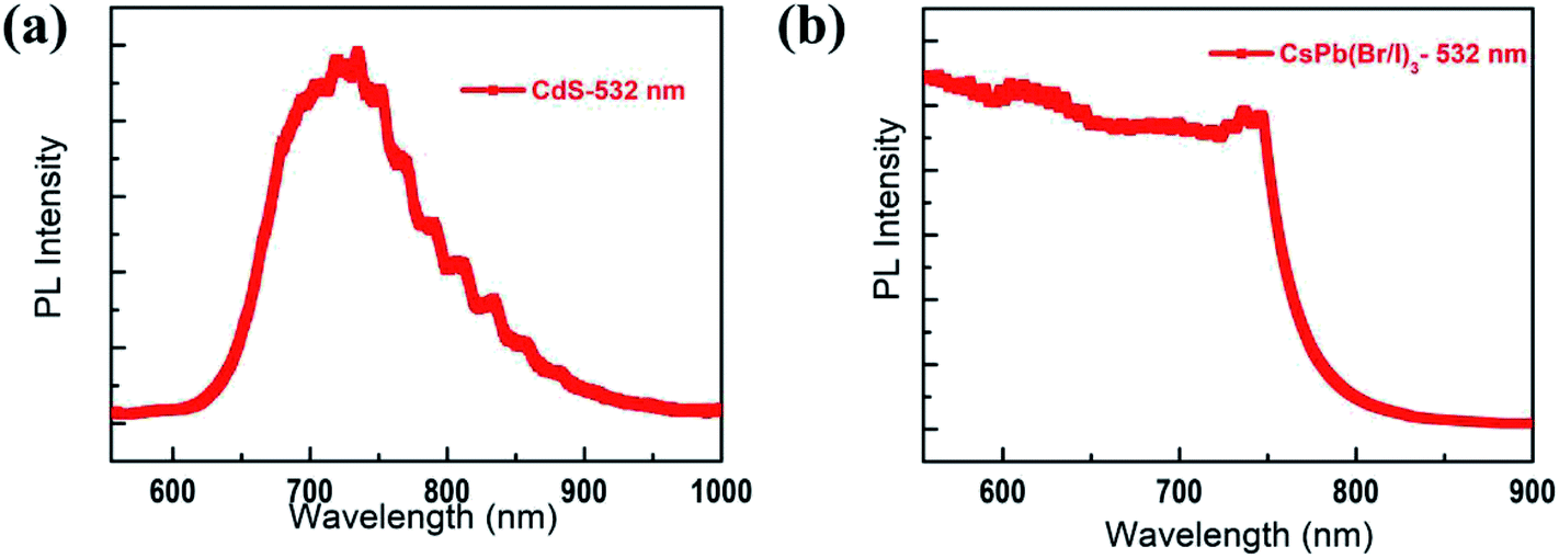 | ||
| Fig. 7 PL spectra of (a) CdS MWs and (b) CsPb(Br/I)3 NCs at an excitation wavelength of 532 nm. | ||
4. Conclusions
Highly efficient and sensitive broadband UV/visible/near-infrared photodetectors were fabricated based on CsPb(Br/I)3 NC/CdS-MW heterostructures. The results showed that introduced CsPb(Br/I)3 NCs effectively improved the light-absorption property of the CsPb(Br/I)3 NC/CdS-MW heterostructures and decreased the charge recombination in the prepared photodetectors due to the formation of a type-II heterojunction. Furthermore, the photogenerated carriers transferred from the CsPb(Br/I)3 NC part to the CdS-MW part through diffusion. Thus, the light-sensing performance in terms of R, EQE, D* was then systematically investigated under 365, 530, 660, 760, and 810 nm. The photodetector based on CsPb(Br/I)3 NC/CdS-MW heterostructures exhibited a distinguished photoelectric performance. Thus, the CsPb(Br/I)3 NC/CdS-MW heterostructures exhibit a great potential for broadband photodetectors, which are important functional components of optoelectronics.Conflicts of interest
There are no conflicts to declare.Acknowledgements
This study was supported by the National Natural Science Foundation of China (11804257), Natural Science Foundation of Hubei Province (2018CFB106), Scientific Research Foundation of Wuhan Institute of Technology (18QD24), Scientific Research Foundation of Wuhan Institute of Technology (XZJJ2020132).References
- Y. Cui, Z. H. Zhong, D. L. Wang, W. U. Wang and C. M. Lieber, Nano Lett., 2003, 3, 149–152 CrossRef CAS.
- C. Y. Yan, J. X. Wang, X. Wang, W. B. Kang, M. Q. Cui, C. Y. Foo and P. S. Lee, Adv. Mater., 2014, 26, 943–950 CrossRef CAS PubMed.
- C. T. Huang, J. H. Song, C. M. Tsai, W. F. Lee, D. H. Lien, Z. Y. Gao, Y. Hao, L. J. Chen and Z. L. Wang, Adv. Mater., 2010, 22, 4008–4013 CrossRef CAS PubMed.
- F. Qian, S. Gradecak, Y. Li, C.-Y. Wen and C. M. Lieber, Nano Lett., 2005, 5, 2287–2291 CrossRef CAS PubMed.
- L. P. Qin, J. Q. Xu, X. W. Dong, Q. Y. Pan, Z. X. Cheng, Q. Xiang and F. Li, Nanotechnology, 2008, 19, 185705 CrossRef PubMed.
- K. T. Nam, D.-W. Kim, P. J. Yoo, C.-Y. Chiang, N. Meethong, P. T. Hammond, Y.-M. Chiang and A. M. Belcher, Science, 2006, 312, 885–888 CrossRef CAS PubMed.
- Z. J. Zhao, C. Y. Xu, L. B. Niu, X. L. Zhang and F. J. Zhang, Laser Photonics Rev., 2020, 14, 2000262 CrossRef CAS.
- S. Y. Liang, Y. Z. Dai, G. Wang, H. Xia and J. H. Zhao, Nanoscale, 2020, 12, 23200–23205 RSC.
- L. Miao and F. J. Zhang, J. Mater. Chem. C, 2019, 7, 1741–1791 RSC.
- X. Li, Y. S. Xu, C. L. Li, Q. Guo, G. Wang, H. Xia, H. H. Fang, L. Shen and H. B. Sun, Adv. Mater., 2020, 32, 2001998 CrossRef PubMed.
- J. Zhao, J. Wang, C. Y. Xu, K. X. Yang, F. G. Zhao, K. Wang, X. L. Zhang and F. J. Zhang, J. Phys. Chem. Lett., 2020, 11, 366–373 CrossRef PubMed.
- X. Zhou, L. Gan, W. M. Tian, Q. Zhang, S. Y. Jin, H. Q. Li, Y. Bando, D. Golberg and T. Y. Zhai, Adv. Mater., 2015, 27, 8035–8041 CrossRef CAS PubMed.
- Z. Zheng, L. Gan, H. Q. Li, Y. Ma, Y. Bando, D. Golberg and T. Y. Zhai, Adv. Funct. Mater., 2015, 25, 5885–5894 CrossRef CAS.
- X. Zhou, Q. Zhang, L. Gan, X. Li, H. Q. Li, Y. Zhang, D. Golberg and T. Y. Zhai, Adv. Funct. Mater., 2016, 26, 704–712 CrossRef CAS.
- D. Wu, Y. Jiang, Y. G. Zhang, Y. Q. Yu, Z. F. Zhu, X. Z. Lan, F. Z. Li, C. Y. Wu, L. Wang and L. B. Luo, J. Mater. Chem., 2012, 22, 23272–23276 RSC.
- T. Gao, Q. Zhang, J. N. Chen, X. Xiong and T. Y. Zhai, Adv. Opt. Mater., 2017, 5, 1700206 CrossRef.
- X. X. Yu, H. Yin, H. X. Li, W. Zhang, H. Zhao, C. Li and M. Q. Zhu, Nano Energy, 2017, 34, 155–163 CrossRef CAS.
- W. Chang, W. P. Li, L. Q. Zhu, H. C. Liu, H. F. Geng, S. S. Xiang, J. M. Liu and H. N. Chen, ACS Appl. Mater. Interfaces, 2016, 8, 33649–33655 CrossRef PubMed.
- Y. Shen, C. Sun, X. Bai, X. Y. Zhang, Y. Wang, Y. D. Wang, H. W. Song and W. W. Yu, ACS Appl. Mater. Interfaces, 2018, 10, 16768–16775 CrossRef PubMed.
- S. Shan, J. H. Li, J. Z. Song, Y. S. Zou, L. M. Xu, J. Xue, Y. H. Dong, C. X. Huo, J. W. Chen, B. N. Han and H. B. Zeng, J. Mater. Chem. C, 2017, 5, 4565–4570 RSC.
- W. Zhang, S. L. Shen, M. Li, L. Y. Li, J. B. Zhang, L. W. Fan, F. Cheng, C. Li, M. Zhu, Z. Kang, J. Su, T. Y. Zhai and Y. H. Gao, Adv. Opt. Mater., 2019, 1801744 CrossRef.
- H. Kwak, D. H. Lim, H. S. Ra, P. Ramasamy and J. S. Lee, RSC Adv., 2016, 6, 65252–65256 RSC.
- H. Dong, Y. Gu, Y. S. Zou, J. Z. Song, L. M. Xu, J. H. Li, J. Xue, X. M. Li and H. B. Zeng, Small, 2016, 12, 5622–5632 CrossRef PubMed.
- F. Li, C. Ma, H. Wang, W. Hu, W. Yu, A. D. Sheikh and T. Wu, Nat. Commun., 2015, 6, 8238 CrossRef PubMed.
- X. He, Y. Qiu and S. Yang, Adv. Mater., 2017, 29, 1700775 CrossRef PubMed.
- L. W. Zhang, S. L. Shen, L. Y. Li, Z. Zhang, N. S. Liu and Y. H. Gao, J. Inorg. Mater., 2019, 34, 37 CrossRef.
- Q. A. Akkerman, V. D'Innocenzo, S. Accornero, A. Scarpellini, A. Petrozza, M. Prato and L. Manna, J. Am. Chem. Soc., 2015, 137, 10276–10281 CrossRef CAS PubMed.
- Y. Su, X. J. Chen, W. Y. Ji, Q. H. Zeng, Z. Y. Ren, Z. S. Su and L. Liu, ACS Appl. Mater. Interfaces, 2017, 9, 33020–33028 CrossRef CAS PubMed.
- K. Ravi, S. Saikia, S. Yadav, V. V. Nawale and A. Nag, ACS Energy Lett., 2020, 5, 1794–1796 CrossRef.
- H. Liu, Y. Tan, M. Cao, H. Hu, L. Wu, X. Yu, L. Wang, B. Sun and Q. Zhang, ACS Nano, 2019, 13, 5366–5374 CrossRef CAS PubMed.
- X. Zhang, X. Wu, X. Liu, G. Chen, Y. Wang, J. Bao, X. Xu, X. Liu, Q. Zhang and K. Yu, J. Am. Chem. Soc., 2020, 142, 4464–4471 CrossRef CAS PubMed.
- H. Liu, X. W. Zhang, L. Q. Zhang, Z. G. Yin, D. G. Wang, J. H. Meng, Q. Jiang, Y. Wang and J. B. You, J. Mater. Chem. C, 2017, 5, 6115 RSC.
- Z. Kang, Y. N. Ma, X. Y. Tan, M. Zhu, Z. Zheng, N. S. Liu, L. Y. Li, Z. G. Zou, X. L. Jiang, T. Y. Zhai and Y. H. Gao, Adv. Electron. Mater., 2017, 1700165 CrossRef.
- J. Fritsche, D. Kraft, A. Thißen, T. Mayer, A. Klein and W. Jaegermann, Thin Solid Films, 2002, 403–404, 252–257 CrossRef CAS.
- F. Lv, Y. B. Xu, H. H. Fang, W. J. Luo, F. J. Xu, L. M. Liu, B. W. Wang, X. F. Zhang, D. Yang, W. D. Hu and A. G. Dong, Nanoscale, 2016, 8, 13589 RSC.
- F. Prins, A. J. Goodman and W. A. Tisdale, Nano Lett., 2014, 14, 6087 CrossRef CAS PubMed.
- W. L. Barnes and P. Andrew, Nature, 1999, 400, 505 CrossRef CAS.
- J. Yuan, S. Najmaei, Z. Zhang, J. Zhang, S. Lei, P. M. Ajayan, B. I. Yakobson and J. Lou, ACS Nano, 2015, 9, 555 CrossRef CAS PubMed.
- R. Calarco, M. Marso, T. Richter, A. I. Aykanat, R. Meijers, A. v. d. Hart, T. Stoica and H. Lüth, Nano Lett., 2005, 5, 981 CrossRef CAS PubMed.
- L. Dou, Y. M. Yang, J. You, Z. Hong, W. H. Chang, G. Li and Y. Yang, Nat. Commun., 2014, 5, 5404 CrossRef CAS PubMed.
Footnote |
| † Electronic supplementary information (ESI) available. See DOI: 10.1039/d1ra00890k |
| This journal is © The Royal Society of Chemistry 2021 |