
 Open Access Article
 This Open Access Article is licensed under a Creative Commons Attribution-Non Commercial 3.0 Unported Licence
A visible-light phototransistor based on the heterostructure of ZnO and TiO2 with trap-assisted photocurrent generation†
Byung Jun Kimab,
Jun Hyung Jeongab,
Eui Young Jungab,
Tae Yeon Kimab,
Sungho Parkab,
Jong-Am Hongc,
Kyu-Myung Leec,
Woojin Jeon ab,
Yongsup Parkcd and
Seong Jun Kang*ab
ab,
Yongsup Parkcd and
Seong Jun Kang*ab
aDepartment of Advanced Materials Engineering for Information and Electronics, Kyung Hee University, Yongin 17104, Republic of Korea. E-mail: junkang@khu.ac.kr; Tel: +82-31-201-3324
bIntegrated Education Program for Frontier Materials (BK21 Four), Kyung Hee University, Yongin 17104, Republic of Korea
cDepartment of Physics and Research Institute for Basic Sciences, Kyung Hee University, Seoul 02447, Republic of Korea
dDepartment of Information Display, Kyung Hee University, Seoul 02447, Republic of Korea
First published on 24th March 2021
Abstract
Visible-light phototransistors have been fabricated based on the heterojunction of zinc oxide (ZnO) and titanium oxide (TiO2). A thin layer of TiO2 was deposited onto the spin-coated ZnO film via atomic layer deposition (ALD). The electrical characteristics of the TiO2 layer were optimized by controlling the purge time of titanium isopropoxide (TTIP). The optimized TiO2 layer could absorb the visible-light from the sub-gap states near the conduction band of TiO2, which was confirmed via photoelectron spectroscopy measurements. Therefore, the heterostructure of TiO2/ZnO can absorb and generate photocurrent under visible light illumination. The oxygen-related-states were investigated via X-ray photoelectron spectroscopy (XPS), and the interfacial band structure between TiO2 and ZnO was evaluated via ultraviolet photoelectron spectroscopy (UPS). Oxygen-related states and subgap-states were observed, which could be used to generate photocurrent by absorbing visible light, even with TiO2 and ZnO having a wide bandgap. The optimized TiO2/ZnO visible-light phototransistor showed a photoresponsivity of 99.3 A W−1 and photosensitivity of 1.5 × 10⁵ under the illumination of 520 nm wavelength light. This study provides a useful way to fabricate a visible-light phototransistor based on the heterostructure of wide bandgap oxide semiconductors.
Introduction
Thin-film transistors (TFTs) based on oxide semiconductors have been commercialized in numerous electronics industries due to excellent electrical characteristics, such as high field effect mobility, low off-current, and high on/off ratio. Oxide semiconductors can be used as a large-scale, flexible, and highly transparent electronics.1–5 Furthermore, oxide semiconductors have been a potential candidate for an active channel material of photosensors.6–8 For these reasons, research on UV phototransistors based on oxide semiconductors has been conducted.9–11 The device with a wide bandgap oxide semiconductor can generate a photocurrent under the illumination of high photon energy, such as UV light. However, it is hard to absorb the low photon energy, such as visible light, and generate a photocurrent due to the wide bandgap (>3.0 eV).To generate photocurrent under visible light illumination using an oxide semiconductor, it is essential to introduce additional absorbing layers on the device, such as two-dimensional materials, metal nanoparticles, organic materials, and quantum dots.12–18 However, heterojunction structure phototransistors have drawbacks such as poor uniformity, interface traps, and defect sites between other absorbing layers and oxide semiconductors.19 In particular, traps at the interface deteriorate electrical characteristics with high-off current, low on/off ratio, and roll-off effects.20 To resolve these problems, heterostructures based on oxide semiconductors have been suggested instead of organic and other nanomaterials on the wide bandgap oxide semiconductor.21,22
In this study, we introduced a heterojunction structure based on the oxide semiconductors of titanium oxide (TiO2) and zinc oxide (ZnO) to fabricate a visible-light phototransistor. A TiO2 layer was deposited onto a spin-coated ZnO via atomic layer deposition (ALD) under various purge time periods of titanium isopropoxide (TTIP) to find an optimal absorbing TiO2 layer. The optimized TiO2 layer on ZnO could absorb the visible light and generate photo-excited electrons from oxygen-related-states via trap-assisted photoelectron generation. These photo-excited electrons could be transferred from TiO2 into the active channel of ZnO. To investigate the origin of the trap-assisted photoelectron generation, X-ray photoelectron spectroscopy (XPS) and ultraviolet photoelectron spectroscopy (UPS) measurements were conducted. Therefore, we suggest an efficient heterostructure composed of TiO2/ZnO for the visible-light phototransistor based on oxide semiconductors.
Result and discussion
Fig. 1a shows a schematic of the visible-light phototransistor with the heterostructure composed of TiO2/ZnO on the SiO2/Si substrate and the ALD process of TiO2. To optimize the process-condition of the TiO2 layer as a stable photo-active channel, process controls for the optimal sub-gap states of TiO2 were conducted according to different purge time periods (0.5, 10, and 20 s) of titanium isopropoxide (TTIP). Table S1† summarizes the saturation field-effect mobilities and electron concentrations. The field effect mobility of TiO2/ZnO TFTs was higher than that of the ZnO TFT due to the bilayer of TiO2/ZnO.23 Also, electron concentration shows a similar tendency with the field effect mobility. Transfer curves of TiO2/ZnO TFTs under various purge time periods of TTIP were measured to confirm the electrical characteristics, as shown in Fig. 1b. TiO2 (purgeTTIP 0.5 s)/ZnO TFT showed poor transfer curve characteristics since the purge process time of TTIP was short and organic residues composed of the carbon groups (C) remained on the TiO2 film during the ALD-process.23 These organic materials cause a current path with an increase in the off current at a negative voltage range and ∼103 on/off ratio.21,24,25 In addition, to determine the origin of the unstable transfer curve characteristics of TiO2/ZnO TFTs, the chemical states of TiO2 films were analyzed with various purge time periods of ALD-TiO2 (0.5, 10, and 20 s). Fourier transform infrared (FT-IR) spectroscopy was performed to investigate the chemical states related to the organic residues of TiO2 on ZnO films. As shown in Fig. S1,† peaks were observed at 1375 and 1019 cm−1, which were attributed to the chemical bonds of TiO2 (–CH3 and C–O, respectively).26 With the decrease in the purge time of ALD-TiO2, the intensity of the peaks increased due to the extra carbon groups of TiO2 during the ALD-process. In particular, an increased intensity of the TiO2 (purgeTTIP 0.5 s) film was observed since excess carbon groups were left on the TiO2. However, TiO2 (purgeTTIP 10 s and 20 s)/ZnO TFTs showed relatively stable transfer characteristics with low leakage current (∼10−11 A) at the negative voltages and 106 on/off ratio compared to the TiO2 (purgeTTIP 0.5 s)/ZnO TFT. These were the reasons why the ligands composed of carbon groups easily broke loose from TTIP, and the ratio of the bonds between Ti and O3 increased in 10 and 20 s of the TTIPpurge time. Therefore, TiO2 (>purgeTTIP 10 s) films are required to decrease the organic residues related to the carbon groups and to enhance the transfer characteristics of the TiO2/ZnO phototransistors.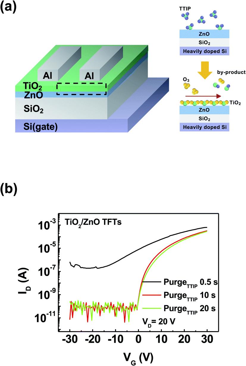 | ||
| Fig. 1 (a) Schematic of the phototransistor with a heterostructure of TiO2 and ZnO with the ALD process of TiO2. (b) Transfer curves of the TiO2/ZnO TFTs according to the change in the TTIP purge time (0.5, 10, and 20 s). | ||
Fig. 2 shows the photoresponse characteristics of ZnO and TiO2/ZnO TFTs with each TTIP purge time at various wavelengths (λ = 635, 520, 450, and 405 nm, P = 4.5 mW cm−2). The transfer curve of ZnO TFT showed photoresponse under the illumination of various wavelengths, as shown in Fig. 2a. It enabled the detection of UV light with 405 nm due to the wide bandgap of ZnO and the migration of photo-electrons from the valence band to the conduction band of ZnO.27 However, it is difficult to absorb visible light, such as 520 and 635 nm, owing to the low photon energy.28 Moreover, an increased photocurrent and negative shift in the threshold voltage (Vth) were observed at the wavelength of 450 nm despite insufficient photon energy. Solution-processed ZnO had numerous defects related to the oxygen vacancies (VO). Ionized VO+ and VO2+ act as shallow donor states, leading to the generation of unexpected photoexcited charge carriers in the bandgap of ZnO by the photon energy.29,30 Fig. 2b shows the transfer curve of TiO2 (purgeTTIP 0.5 s)/ZnO TFT under numerous wavelengths. An inferior photoresponse was observed at the visible light since the device showed a high leakage current path with unstable transfer characteristics. TiO2 (purgeTTIP 10 s)/ZnO TFT showed a remarkable change in the photoresponse at the 520 nm wavelength light with an increased Iphoto/Idark of ∼105 and −9.8 V of negative shift Vth, as shown in Fig. 2c. Photo-excited electrons were generated from the oxygen-related-states of TiO2 and then transferred into the conduction band of ZnO.31 Also, much increased photocurrent was observed at the wavelengths of 450 and 405 nm, more than that of 520 nm due to the additionally generated photoexcited electrons from ZnO and TiO2. In Fig. 2d, a small photocurrent and negative shift Vth were observed at the wavelength of 520 nm since the TTIP purge time of 20 s enabled the separation of the ligands and carbon residues from TTIP and enhanced the bonds between Ti atoms and O atoms to form a stable TiO2 film. These results indicate that the TiO2/ZnO visible light phototransistor was optimized at the TTIP purge time of 10 s.
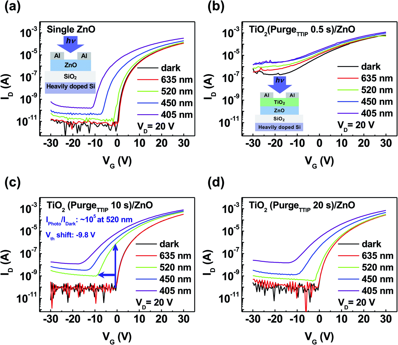 | ||
| Fig. 2 Transfer curve characteristics with the illumination of various wavelengths of light for (a) ZnO phototransistor and TiO2/ZnO phototransistors according to the different TTIP purge time periods of (b) 0.5, (c) 10, and (d) 20 s at VD = 20 V. | ||
To investigate an interfacial electronic band structure at the optimized TiO2 (purgeTTIP 10 s)/ZnO interface, UPS measurements were conducted, as shown in Fig. 3a. UPS spectra of the secondary electron cutoff (SEC) region and valence region were obtained. The incident energy of the UV source (He I) was 21.2 eV. EC is the conduction band maximum energy level; Evac is the vacuum level energy. The work function was obtained from the fitting of the UPS spectra. The work functions of ZnO and TiO2 (purgeTTIP 10 s) were 4.07 eV and 4.41 eV, respectively. The energy level between Fermi energy (EF) and valence band maximum (VBM) of ZnO and TiO2 (purgeTTIP 10 s) were 3.02 and 3.06 eV, respectively. The band gaps (Eg = EC − Ev) of ZnO and TiO2 (purgeTTIP 10 s) were calculated from the Tauc's plot based on the UV-Vis spectroscopy measurement, as shown in Fig. S2.† The band gaps of ZnO and TiO2 (purgeTTIP 10 s) were 3.24 and 3.30 eV, respectively. Fig. 3b shows the band alignment between ZnO and TiO2 (purgeTTIP 10 s). The small band offset (0.02 eV) between the conduction band of ZnO and TiO2 (purgeTTIP 10 s) was measured. A favorable interfacial band alignment between ZnO and TiO2 (purgeTTIP 10 s) was achieved, and efficient photo-excited electron transport from TiO2 (purgeTTIP 10 s) into the ZnO layer could be expected.
 | ||
| Fig. 3 (a) UPS spectra, and (b) schematic of the band alignment between the ZnO and TiO2 (TTIP 10 s) films. | ||
XPS was performed to investigate the oxygen-related-states of TiO2 according to numerous TTIP purge time periods (0.5, 10, and 20 s). Fig. S3a† shows the XPS survey spectra of ZnO, TiO2 layers with variation in the purge time periods of TTIP. In the XPS spectra, the O 1s, Zn 2p, and Ti 2p peaks were intensively observed. However, Zn 2p was negligibly observed in the TiO2/ZnO samples since the TiO2 film was deposited on the ZnO film. The O 1s peak was analyzed to confirm the oxygen-related-states of the TiO2 layers. As shown in Fig. 4, the O 1s peaks are deconvoluted into three peaks at 530.1, 531.2, and 532.2 eV, which are attributed to the Ti–O bond of the lattice oxygen, VO in the TiO2 layer, and hydroxides species (–OH) on the film surface, respectively.32 With the increase in the purge time of TTIP, the Ti–O bonds at the lattice oxygen increased, and the relative area ratios were 85.14, 86.37, and 89.08% at the TTIP purge time periods of 0.5, 10, and 20 s, respectively.33 With the increase in the TTIP purge time, the relative area ratio of VO decreased (9.73, 8.76, and 6.57% at TTIP purge time periods of 0.5, 10, and 20 s, respectively), indicating that subgap-states related to VO exist at TiO2.34 As shown in Fig. S3b–d,† the Ti 2p peaks are deconvoluted. The peaks at 463.4 and 457.8 eV are assigned to Ti3+ 2p1/2 and Ti3+ 2p3/2, respectively. Also, the peaks at 464.9 and 458.8 eV are assigned to Ti4+ 2p1/2 and Ti4+ 2p3/2, respectively.35 Table 1 summarizes the binding energy and area ratio of Ti 2p1/2 and Ti 2p3/2. According to the TTIP purge time periods (0.5, 10, and 20 s) of TiO2, the area ratios of Ti3+ at Ti 2p1/2 are 48.65, 47.82, and 46.50%, and the area ratios of Ti3+ at Ti 2p3/2 are 3.29, 2.47, and 0.91%. As the purge time of TTIP increased, the area ratio of Ti3+ decreased, which corresponded to oxygen vacancies with Ti3+ from deficient bonding between Ti and O. However, the area ratio of Ti4+ gradually increased.36 Therefore, it indicates that the TiO2 with the TTIP purge time of 10 s was a more useful film than that of the TTIP purge time of 0.5 s for the visible-light phototransistor, as shown in Fig. 2b. The optimized oxygen-related defects by VO in the bandgap of TiO2 could excite photo-generated electrons in TiO2 by the illumination of visible light.37–39 Therefore, it was found that the process of 10 s of TTIP purge time during TiO2 deposition was appropriate for a visible-light phototransistor.
 | ||
| Fig. 4 O 1s spectra of TiO2 on the ZnO film with different TTIP purge time periods of (a) 0.5, (b) 10, and (c) 20 s. | ||
| Ti 2p1/2 [eV (%)] | Ti 2p3/2 [eV (%)] | |||
|---|---|---|---|---|
| Ti3+ | Ti4+ | Ti3+ | Ti4+ | |
| TiO2 (purgeTTIP 0.5 s)/ZnO | 463.38 (48.65) | 464.92 (51.35) | 457.83 (3.29) | 458.83 (96.71) |
| TiO2 (purgeTTIP 10 s)/ZnO | 463.38 (47.82) | 464.90 (52.18) | 457.83 (2.47) | 458.80 (97.53) |
| TiO2 (purgeTTIP 20 s)/ZnO | 463.37 (46.50) | 464.89 (53.50) | 457.75 (0.91) | 458.77 (99.09) |
UV-visible spectroscopy measurements were conducted to investigate the photoresponse by subgap-states under visible light, as shown in Fig. 5a. ZnO and TiO2 (purgeTTIP 10 s)/ZnO films were measured at the wavelength ranging from 350 to 800 nm. Compared to the ZnO film, the intensity of absorbance remarkably increased at the TiO2 (purgeTTIP 10 s)/ZnO film under visible light (λ = 400 to 700 nm) by the subgap-states of the TiO2.40 Moreover, Fig. 5b shows the UPS spectra of ZnO and TiO2 (purgeTTIP 10 s)/ZnO films. The difference in the intensity indicates that the subgap-states near the valence band edge in the TiO2 (purgeTTIP 10 s)/ZnO film exist more than those of the ZnO film in the range from 0 to 3.5 eV.41,42 These results suggest that subgap-states in the TiO2 (purgeTTIP 10 s)/ZnO film can induce visible light absorption. Therefore, it indicates that electrons at the subgap-states and oxygen-related states can be trapped near the CBM and VBM levels of the TiO2 film. As shown in Fig. 5c, these trapped-electrons can generate photoexcited electrons by trap-assisted generation under low photon energy, such as the visible light. Then, photoexcited electrons near the CBM of TiO2 can be smoothly transferred into ZnO with a favorable band alignment between ZnO and TiO2 due to the minimal difference in the CBM energy level (0.08 eV). As a result, the increased number of the photoexcited electrons by trapped electrons at the subgap-states of the TiO2 causes the photocurrent under the visible light.
 | ||
| Fig. 5 (a) Absorption spectra of the ZnO and TiO2 (TTIP 10 s)/ZnO films. The inset shows the absorption spectra from 400 to 700 nm. (b) UPS spectra of the ZnO and TiO2 (TTIP 10 s)/ZnO films. (c) Schematic of the photoexcited charge transport mechanism at the interface between ZnO and TiO2 (TTIP 10 s) with the illumination of light. | ||
Fig. 6a shows the photoresponsivity of ZnO and TiO2 (purgeTTIP 10 s)/ZnO phototransistors under the exposure at the wavelength of 520 nm as a function of VG and VD = 20 V, which was plotted using the equation:

where Ilight is the current in the phototransistor under the exposure of visible light, and Idark is the dark current.19 The photosensitivity of the TiO2 (purgeTTIP 10 s)/ZnO phototransistor was superior to that of the ZnO phototransistor under visible light illumination. The maximum photosensitivity of the TiO2 (purgeTTIP 10 s)/ZnO phototransistor was 1.5 × 10⁵. To confirm the photomodulation characteristics of the TiO2 (purgeTTIP 10 s)/ZnO phototransistor, the on/off photoresponse characteristic was measured at an illumination of a periodic light signal of 520 nm with 0.5 Hz, VG = −15 V, and VD = 20 V. As shown in Fig. 6c, the device periodically responded to the periodic light illumination. The result indicates that the visible light can excite trapped-electrons from the subgap-states and oxygen-related-states to the CBM of TiO2.21 The result from the experiment indicates a feasible way to fabricate a visible-light-sensitive phototransistor based on the heterostructure composed of a wide bandgap oxide semiconductor with oxygen-related-states.

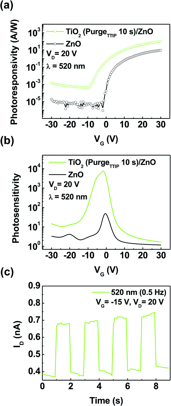 | ||
| Fig. 6 (a) Photoresponsivity and (b) photosensitivity of the ZnO and TiO2 (TTIP 10 s)/ZnO phototransistors at VD = 20 V under the visible light illumination (λ = 520 nm, P = 4.5 mW cm−2). (c) Photoresponse characteristics of the TiO2 (TTIP 10 s)/ZnO phototransistors under 0.5 Hz periodic illumination of 520 nm wavelength light. | ||
Conclusion
A visible light phototransistor based on the heterostructure of ALD-TiO2 and a spin-coated ZnO has been fabricated. The device generated a photocurrent under the exposure visible light due to the oxygen-related-states and subgap-states of TiO2. To investigate the origin of photocurrent generation, UPS, XPS, and UV-visible spectroscopy measurements were performed. The oxygen-related-states enabled the generation of a photocurrent under visible light illumination on the device even when the active channel materials have a wide bandgap. The favorable band alignment between ZnO and TiO2 (purgeTTIP 10 s) was confirmed by the measurement of UPS for the efficient charge transfer between TiO2 and ZnO. Therefore, the TiO2 (purgeTTIP 10 s)/ZnO phototransistor exhibited a photoresponsivity of 99.3 A W−1, photosensitivity of 1.5 × 10⁵, and Iphoto/Idark ratio of ∼105. Moreover, it was hard to observe a persistent photocurrent effect during the modulation of the device with periodic visible light illumination. The result provides a useful way to fabricate a visible light phototransistor based on the heterostructure of wide bandgap oxide semiconductors.Experimental
ZnO solution synthesis
A ZnO solution was synthesized using 0.0813 g of ZnO powder (Sigma Aldrich, 99.999%) and 12 mL ammonium hydroxide solvent (Alfa Aesar, 99.9%). Then, the ZnO solution was stirred for 30 min in the ambient atmosphere. The ZnO solution was refrigerated for 5 h to increase the solubility of the ZnO powder in the ammonium hydroxide solvent.43Fabrication of the device
To fabricate the ZnO phototransistor with an ALD-TiO2, a ZnO film was spin-coated onto a SiO2 (100 nm)/Si substrate at 3000 rpm for 30 s. Then, the ZnO film was annealed at 300 °C for 1 h under ambient atmosphere to remove the ammonium hydroxide solvent. Subsequently, a TiO2 film was deposited onto the ZnO film via the ALD process with titanium isopropoxide (TTIP) and ozone. The ALD system was operated at an Ar flow rate of 150 sccm and 300 cyc as well as process variations to purge time of TTIP. The process was maintained at 250 °C of the substrate temperature. Finally, 100 nm-thick aluminum electrodes for source/drain were deposited onto the substrate using a thermal evaporator with a shadow mask. The shadow mask was a channel with a length (L) of 100 and width (W) of 1000 μm.Characterization and measurement of the film and device
A semiconductor parameter analyzer (HP 4145B) and probe station were used to investigate the transfer curves of the phototransistors. The optoelectrical characteristics were measured under dark conditions and exposure to the various illumination wavelengths (λ) of 405, 450, 520, 650, and 780 nm, with an illumination power of approximately 4.5 mW cm−2. A UV-visible spectrometer (Jasco V-570) was used to record the absorbance spectra of the ZnO and TiO2/ZnO film. XPS and UPS measurements were performed to investigate the interfacial electronic structure between ZnO and TiO2 using a modified KRATOS AXIS NOVA system with an Al Kα (1486.6 eV) source and a He-I line (21.22 eV) source at a base pressure of 5 × 10⁻⁹ torr.Conflicts of interest
There are no conflicts to declare.Acknowledgements
This work was supported by a research project grant from the National Research Foundation of Korea (NRF-2020R1F1A1067756 and 2020R1A6A1A03048004).Notes and references
- K. Nomura, Science, 2003, 300, 1269–1272 CrossRef CAS PubMed.
- H. Lee, K. S. Chang, Y. J. Tak, T. S. Jung, J. W. Park, W.-G. Kim, J. Chung, C. B. Jeong and H. J. Kim, J. Inf. Disp., 2017, 18, 131–135 CrossRef CAS.
- K. Nomura, H. Ohta, A. Takagi, T. Kamiya, M. Hirano and H. Hosono, Nature, 2004, 432, 488–492 CrossRef CAS PubMed.
- S. Hong, J. W. Park, H. J. Kim, Y. Kim and H. J. Kim, J. Inf. Disp., 2016, 17, 93–101 CrossRef CAS.
- B. D. Ahn, H. S. Shin, G. H. Kim, J.-S. Park and H. J. Kim, Jpn. J. Appl. Phys., 2009, 48, 03B019 CrossRef.
- A. Nathan, S. Lee, S. Jeon and J. Robertson, J. Disp. Technol., 2014, 10, 917–927 CAS.
- W.-G. Kim, Y. J. Tak and H. J. Kim, J. Inf. Disp., 2018, 19, 39–43 CrossRef CAS.
- S.-E. Ahn, I. Song, S. Jeon, Y. W. Jeon, Y. Kim, C. Kim, B. Ryu, J.-H. Lee, A. Nathan, S. Lee, G. T. Kim and U.-I. Chung, Adv. Mater., 2012, 24, 2631–2636 CrossRef CAS PubMed.
- Z. Tao, X. Liu, W. Lei and J. Chen, Mater. Lett., 2018, 228, 451–455 CrossRef CAS.
- H. Choi, S. Seo, J.-H. Lee, S.-H. Hong, J. Song, S. Kim, S.-Y. Yim, K. Lee, S.-J. Park and S. Lee, J. Mater. Chem. C, 2018, 6, 6014–6022 RSC.
- D.-K. Kwon, Y. Porte, K. Y. Ko, H. Kim and J.-M. Myoung, ACS Appl. Mater. Interfaces, 2018, 10, 31505–31514 CrossRef CAS PubMed.
- X. Xu, L. Yan, T. Zou, R. Qiu, C. Liu, Q. Dai, J. Chen, S. Zhang and H. Zhou, ACS Appl. Mater. Interfaces, 2018, 10, 44144–44151 CrossRef CAS PubMed.
- H. Yoo, W.-G. Kim, B. H. Kang, H. T. Kim, J. W. Park, D. H. Choi, T. S. Kim, J. H. Lim and H. J. Kim, ACS Appl. Mater. Interfaces, 2020, 12, 10673–10680 CrossRef PubMed.
- J. E. Cho, J. Yu and S. J. Kang, Curr. Appl. Phys., 2016, 16, 1560–1563 CrossRef.
- J. Yu, B. J. Kim, S. Park, I. K. Han and S. J. Kang, J. Appl. Phys., 2018, 57, 044001 CrossRef.
- J. Yu, S. W. Shin, K.-H. Lee, J.-S. Park and S. J. Kang, J. Vac. Sci. Technol., B: Nanotechnol. Microelectron.: Mater., Process., Meas., Phenom., 2015, 33, 061211 Search PubMed.
- D. Kufer and G. Konstantatos, ACS Photonics, 2016, 3, 2197–2210 CrossRef CAS.
- Y. S. Rim, K.-C. Ok, Y. M. Yang, H. Chen, S.-H. Bae, C. Wang, Y. Huang, J.-S. Park and Y. Yang, ACS Appl. Mater. Interfaces, 2016, 8, 14665–14670 CrossRef CAS.
- B. J. Kim, S. Park, T. Y. Kim, E. Y. Jung, J.-A. Hong, B.-S. Kim, W. Jeon, Y. Park and S. J. Kang, J. Mater. Chem. C, 2020, 8, 16384–16391 RSC.
- Y. S. Rim, Y. M. Yang, S.-H. Bae, H. Chen, C. Li, M. S. Goorsky and Y. Yang, Adv. Mater., 2015, 27, 6885–6891 CrossRef CAS PubMed.
- J. Chung, Y. J. Tak, W.-G. Kim, B. H. Kang and H. J. Kim, ACS Appl. Mater. Interfaces, 2019, 11, 38964–38972 CrossRef CAS PubMed.
- H. Yoo, W.-G. Kim, B. H. Kang, H. T. Kim, J. W. Park, D. H. Choi, T. S. Kim, J. H. Lim and H. J. Kim, ACS Appl. Mater. Interfaces, 2020, 12, 10673–10680 CrossRef PubMed.
- J. S. Kim, S. W. Cho, D. I. Kim, B. U. Hwang, Y. G. Seol, T. W. Kim and N.-E. Lee, J. Nanosci. Nanotechnol., 2014, 14, 8596–8601 CrossRef CAS PubMed.
- Y. S. Rim, W. H. Jeong, D. L. Kim, H. S. Lim, K. M. Kim and H. J. Kim, J. Mater. Chem., 2012, 22, 12491 RSC.
- Y.-H. Kim, J.-S. Heo, T.-H. Kim, S. Park, M.-H. Yoon, J. Kim, M. S. Oh, G.-R. Yi, Y.-Y. Noh and S. K. Park, Nature, 2012, 489, 128–132 CrossRef CAS PubMed.
- Z. Liu, Z. Jian, J. Fang, X. Xu, X. Zhu and S. Wu, Int. J. Photoenergy, 2012, 2012, 8 Search PubMed.
- S. Park, B. J. Kim, S. J. Kang and N.-K. Cho, J. Korean Phys. Soc., 2018, 73, 1351–1355 CrossRef CAS.
- Y. S. Rim, B.-D. Ahn, J.-S. Park and H. J. Kim, J. Phys. D: Appl. Phys., 2013, 47, 045502 CrossRef.
- Y. J. Tak, D. H. Yoon, S. Yoon, U. H. Choi, M. M. Sabri, B. D. Ahn and H. J. Kim, ACS Appl. Mater. Interfaces, 2014, 6, 6399–6405 CrossRef CAS PubMed.
- H. S. Kang, J. S. Kang, J. W. Kim and S. Y. Lee, J. Appl. Phys., 2004, 95, 1246–1250 CrossRef CAS.
- Y.-C. Shen, C.-Y. Tung, C.-Y. Huang, Y.-C. Lin, Y.-G. Lin and R.-H. Horng, ACS Appl. Electron. Mater., 2019, 1, 783–788 CrossRef CAS.
- K. Shen, K. Wu and D. Wang, Mater. Res. Bull., 2014, 51, 141–144 CrossRef CAS.
- H.-H. Hsu, C.-H. Cheng, P. Chiou, Y.-C. Chiu, C.-Y. Chang and Z.-W. Zheng, Solid-State Electron., 2014, 99, 51–54 CrossRef CAS.
- B. H. Kang, W.-G. Kim, J. Chung, J. H. Lee and H. J. Kim, ACS Appl. Mater. Interfaces, 2018, 10, 7223–7230 CrossRef CAS.
- J. Tian, Y. Leng, H. Cui and H. Liu, J. Hazard. Mater., 2015, 299, 165–173 CrossRef CAS PubMed.
- X. Zhang, H. Tian, X. Wang, G. Xue, Z. Tian, J. Zhang and Z. Zou, Mater. Lett., 2013, 100, 51–53 CrossRef CAS.
- N. Mintcheva, S. Yamaguchi and S. A. Kulinich, Materials, 2020, 13, 719 CrossRef CAS.
- B. Bharti, S. Kumar, H.-N. Lee and R. Kumar, Sci. Rep., 2016, 6, 32355 CrossRef CAS PubMed.
- Y. Liu, J. Wang, P. Yang and K. Matras-Postolek, RSC Adv., 2015, 5, 61657–61663 RSC.
- B. Ozden, C. Yang, F. Tong, M. P. Khanal, V. Mirkhani, M. H. Sk, A. C. Ahyi and M. Park, Appl. Phys. Lett., 2014, 105, 172105 CrossRef.
- H. Tang, Y. Kishida, K. Ide, Y. Toda, H. Hiramatsu, S. Matsuishi, S. Ueda, N. Ohashi, H. Kumomi, H. Hosono and T. Kamiya, ECS J. Solid State Sci. Technol., 2017, 6, P365 CrossRef CAS.
- L. Gao, Y. Li, J. Ren, S. Wang, R. Wang, G. Fu and Y. Hu, Appl. Catal., B, 2017, 202, 127–133 CrossRef CAS.
- J. J. Richardson and F. F. Lange, Cryst. Growth Des., 2009, 9, 2570–2575 CrossRef CAS.
Footnote |
| † Electronic supplementary information (ESI) available. See DOI: 10.1039/d1ra00801c |
| This journal is © The Royal Society of Chemistry 2021 |