
 Open Access Article
 This Open Access Article is licensed under a Creative Commons Attribution-Non Commercial 3.0 Unported Licence
Formation of self-assembled Gd2O3 nanowire-like structures during epitaxial growth on Si(001)
Philipp Gribisch * and
Andreas Fissel
* and
Andreas Fissel
Institute of Electronic Materials and Devices, Leibniz University Hannover, Schneiderberg 32, 30167 Hannover, Germany. E-mail: gribisch@mbe.uni-hannover.de
First published on 13th May 2021
Abstract
The structural and morphological properties of gadolinium oxide (Gd2O3) grown at high temperatures with molecular beam epitaxy on Si(001) were investigated for different stages of growth. The Gd2O3 layers were grown at 850 °C with different oxygen partial pressures and substrate miscuts. RHEED and XRD investigations indicate an initial formation of silicide and a subsequent transformation into cubic Gd2O3 with (110) orientation. The surface exhibits nanowire-like structures oriented orthogonally along with the [110] directions of the substrate, as indicated by AFM. Since on 4° off-cut Si(001) substrates the nanowire-like structures are mainly oriented in only one [110] direction, the orientation of the formed Gd2O3 structures seems to be related to the dimer orientation of the (2 × 1) reconstructed Si(001) surface. The density and length of the nanowire-like structures can be tuned by a change in oxygen partial pressure. The results were discussed in terms of different physical effects, where a combination of desorption of silicon and the formation of a silicide layer in the initial stage of growth could be the reason for the growth behaviour, which is also supported through TEM investigations.
Introduction
Rare earth oxides (REOs) gained lots of attention during the past years due to their broad field of applications,1 such as catalysts in the automotive industry,2 as additives in the glass industry,3 in ceramics4 and additives in batteries.5 They can be also used in high-energy solid-state laser systems and scintillators.6,7 In microelectronic applications, they can be used as alternative gate dielectrics to improve the performance of Si-based8 and GaN-based9 metal oxide semiconductor (MOS) transistors.The physical properties of the REOs are the crucial factor for their applicability, as dielectric properties, bandgap and alignment, thermodynamic and chemical stability in contact with the substrate and surface morphology. All these properties can be influenced by the manufacturing conditions, wherefore the investigations of the influence of fabrication parameters on the structural and morphological properties of rare earth oxides are important.
Most of the REOs exhibit a chemical and thermodynamic stability in contact with silicon and have a low lattice mismatch, which enable the possibility of epitaxial growth.10,11
The epitaxial growth of several REOs on silicon was carried out during the last decades.12–16 During the growth of different REOs, as Pr2O3, Nd2O3, Gd2O3, on Si(001) at standard growth temperatures (Tg ≈ 600 °C), the crystal structures of the layer usually becomes cubic with (110) orientation and smooth surface morphology.17–19 For the growth at lower temperatures on Si(001) also different crystal structures with other orientations can be stabilized.20 On Si(111) also smooth layers with the cubic structure and (111) orientation can be realized.21,22 Detailed investigations on the growth of REOs at higher temperatures (Tg ≫ 600 °C) are still missing.
In our previous studies, first experiments of high-temperature growth were presented, where interesting growth features, such as the formation of nanowire-like structures growing orthogonal along the [110] direction of the substrate, were observed.20
Nanostructured rare earth oxides are the most common rare earth nanomaterials, which are also the most widely studied.23
Rare earth oxides with one-dimensional structures represent a particularly interesting class of materials for various applications, involving, for example, optical displays, optical communication, UV shielding, medical diagnostics, and efficient catalysis24–31 because of their unique electronic, optical, magnetic, and catalytic properties.32–35
Various synthetic strategies were developed and successfully used to prepare many rare earth oxide nanostructures with diverse well-defined morphologies, such as zero-dimensional (0D), one-dimensional (1D), two dimensional (2D) and three-dimensional (3D) nanostructures.36–40
However, synthesizing shape-controlled rare earth oxide nanostructures on Si has not been reported so far.
In this work, we report on a detailed investigation of the nanostructure formation during the growth with molecular beam epitaxy. The influence of growth conditions, such as oxygen partial pressure and growth time, as well as the influence of off-cut Si(001) substrates on the nanowire-like structure formation, were investigated. The layer structure and morphology are investigated with several growth characterization techniques. Based on that, the formation process is discussed in the framework of different physical effects.
Experimental
The Gd2O3 layers were grown on 100 mm silicon (001) substrates doped with boron and a resistivity between 0.02 and 0.75 Ω cm using a multi-chamber solid source molecular beam epitaxy (MBE) system (DCA Instruments) with an average growth rate of 0.2 nm min−1 and growth temperature of 850 °C. Before transferring in the MBE system, the substrates were chemically cleaned with HF and ozone treatment to remove the native oxide and organic impurities on the surface. Prior to the growth of Gd2O3, the Si(001) surface was cleaned by a thermal preparation at 750 °C while a slight silicon flux was introduced as long as the surface exhibits a well-defined (2 × 1) reconstructed surface, as indicated by RHEED. The source material consists of granular Gd2O3, which was evaporated using electron beam heating. Furthermore, additional oxygen was introduced in the growth chamber using a piezo leakage valve to adjust the oxygen partial pressure during the growth. The growth process was in situ monitored with reflection high-energy electron diffraction (RHEED). The layer thickness was approximated with X-ray reflectivity (XRR). The crystal structure and the layer orientation were analyzed with high-resolution X-ray diffraction (HRXRD) measurements and performed with a Bruker AXS D8 Discover diffractometer in Bragg–Brentano geometry with an asymmetrical Ge(220) four-bounce monochromator to select the CuKα1 radiation. Here different XRD scan techniques were performed including symmetric 2θ/ω-scans and φ-scans of asymmetrical reflections and in grazing incidence XRD (GIXRD) configuration. For a further structural investigation transmission electron microscopy (TEM) was performed. The surface morphology was investigated with atomic force microscopy (AFM) in contact mode. For a further evaluation of the surface of the samples, scanning electron microscopy (SEM) was used.Results
In the following, the results of the epitaxial growth of Gd2O3 will be evaluated for different stages.Initial stage of growth
First, the Gd2O3 layer formation in the initial stage of growth was investigated, while growing Gd2O3 on Si(001) for different time referring to different nominal thicknesses.Gd2O3 growth was performed at pO2 = 5·10−7 mbar with nominal thicknesses of 1, 2 and 3 nm. RHEED images were taken after growth in different directions of the substrate and are shown in Fig. 1. The (2 × 1) superstructure spots related to the Si(001) surface have disappeared completely. In comparison to the RHEED pattern of the initially (2 × 1) reconstructed surface, the RHEED image of the 1 nm thick Gd2O3 layer in [110] direction exhibits a superposition of streaky and spotty patterns (Fig. 1a). A streaky RHEED pattern is an indication of a slightly stepped smooth surface of the layer. The reciprocal lattice rods broaden to a certain thickness, wherefore the Ewald sphere is intersected in streaks.41
 | ||
| Fig. 1 RHEED images taken after the growth of the Gd2O3 layers at pO2 = 5·10−7 mbar with 1 nm nominal thickness (a) in [110] direction and (b) in [100] direction of the substrate and with 3 nm nominal thickness (c) in [110] direction and (d) in [100] direction. | ||
The RHEED pattern of the 1 nm thick Gd2O3 layer in [100] direction of the substrate (Fig. 1b) shows apart from the main reflections streaks, which split up in a certain angle. This phenomenon can be attributed to surface line defects, like atomic steps.42,43 These reflections are termed as fan-out streaks and proceed along with the [110] directions. Due to the scattering of the electrons at the surface line defects, the reciprocal lattice rods degenerate into two-dimensional areas. The intersection with the Ewald sphere causes such a RHEED pattern.42 If the electron beam is oriented along with the atomic steps (line defect), this leads to usual streaks. If the electron beam is oriented at an angle of 45° to the step, the fan-out streaks appear.43 Since such phenomenon is not reported for the growth at lower growth temperatures, it can be suggested that the formation of surface line defects is due to processes occurring only at high growth temperatures.
The RHEED patterns of the 3 nm thick Gd2O3 layer show a different behaviour (Fig. 1c and d). The reflections of the RHEED pattern in [110] direction (Fig. 1c) are more spotty-like in comparison to the pattern of the 1 nm thick Gd2O3 layer. The transformation to spotty reflections and the increasing number of reflections apart from the Laue circles indicate an increase in surface roughness. The RHEED pattern in [100] direction of the substrate does not show the fan-out streaks and consists of weak mixed streaky and spotty reflections (Fig. 1d). Overall the pattern is quite similar to the RHEED pattern reported for the growth of cubic Gd2O3 with a (110) orientation at lower temperatures,19 wherefore such a cubic structure of the Gd2O3 layer can be assumed, however, with higher surface roughness.
From the RHEED investigations in the initial stage of the growth, it can be concluded that Gd2O3 layer formation on Si(001) at 850 °C shows a change in growth mode at the beginning of layer growth. It can be suggested that the surface roughens in the initial stage of the growth of the Gd2O3 and that subsequent the Gd2O3 grows in (110) direction. Details will be discussed in the next chapter.
Furthermore, the layers were investigated with XRD measurements in the symmetric 2θ/ω configuration. In the XRD measurement of the Gd2O3 layer with a nominal thickness of 1 nm (Fig. 3), only one peak with very low intensity is visible besides the quasi-forbidden Si002 reflection. However, the peak related to the grown layer does not fit any known reflection of Gd2O3. The peak position was approximated with a Gaussian function with the maximum at 2θ ≈ 26.2°, which is close to the 10-10/004 reflection of hexagonal/orthorhombic GdSi2, based on crystallographic data44,45 and calculated with the program Vesta.46
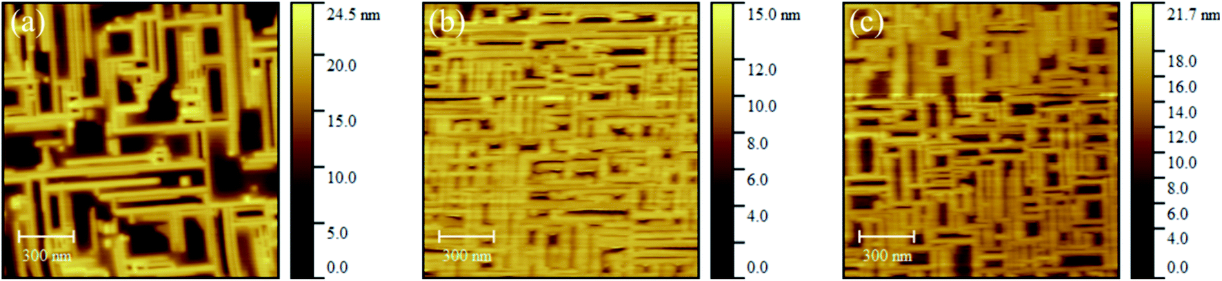 | ||
| Fig. 2 AFM images of the Gd2O3 layers grown at pO2 = 5·10−7 mbar with nominal thicknesses (a) 1 nm (b) 2 nm (c) 3 nm. | ||
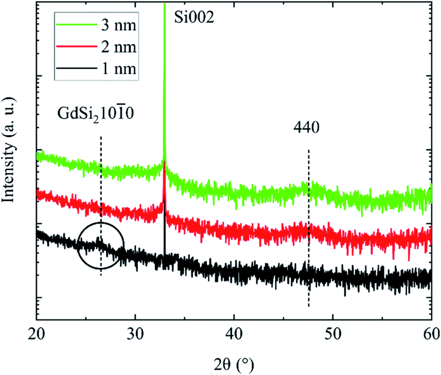 | ||
| Fig. 3 Symmetric 2θ/ω measurements of the Gd2O3 layers grown at pO2 = 5·10−7 mbar with nominal thickness from 1–3 nm. The forbidden Si002 reflection is caused by “Umweganregung”.47 | ||
This observation indicates a silicide formation in the initial stage of growth. However, the intensity of the peak is only slightly above the noise level in accordance with the low thickness.
The XRD measurements of the Gd2O3 layers with a nominal thickness of 2 nm and 3 nm show only one additional weak reflection around 2θ ≈ 47.5°, which can be attributed to the 440 reflection of cubic Gd2O3. The reflection around 2θ ≈ 26° is not visible anymore. This behaviour indicates the growth of the Gd2O3 in the cubic crystal structure and (110) orientation and the absence of a silicide in the layers of 2 nm and 3 nm nominal thickness.
Furthermore, the layers were investigated with AFM to evaluate the surface morphology (Fig. 2). The surface of the Gd2O3 layer with 1 nm nominal thickness shows nanowire-like structures, which are oriented orthogonal to each other in the equivalent [110] directions (Fig. 2a), as established in relation to the Si(001) substrate flats. The height scale shows a height difference up to 25 nm, which is astonishing because only nominal 1 nm was deposited, wherefore a significant transfer of material at the surface around the nanowire-like structures should has occurred. The AFM images of the Gd2O3 layers with nominal thicknesses of 2 nm and 3 nm (Fig. 2b and c) show a similar surface but with a higher density of the nanowire-like structures. The RMS roughness values were calculated with the software Gwyddion using 5 AFM images for each sample and are summarized in Table 1. The RMS values range from around 5 nm for the sample with 1 nm thickness to around 2 nm for the other samples which further supports the observation of a rough surface.
Based on the XRD investigation, it can be suggested that a silicide is forming at the beginning of the growth. For a silicide formation, the silicon from the substrate has to react with the Gd atoms at the surface and in view of the height of the structures, trench formation around the structures can be expected. The formation of these structures will be discussed later in the manuscript.
Later stage of growth
For further evaluation of the growth at high temperatures, Gd2O3 layers with higher nominal thickness were grown with different oxygen partial pressure. Furthermore, the influence of a 4° miscut substrate on the layer morphology was also investigated.The RHEED image of the Gd2O3 layer grown at pO2 = 2·10−7 mbar shows a sharp and spotty pattern (Fig. 4a), which indicates crystalline growth and a rough (three dimensional, 3D) surface morphology. The RHEED pattern of the sample grown at a higher oxygen partial pressure (pO2 = 5·10−7 mbar) (Fig. 4b) is almost identical. Next to the main reflection to the middle of the RHEED pattern an additional spot with very weak intensity is visible. This would be an indication for the growth of the cubic structure with (110) orientation with two orthogonal domains, as already reported for Gd2O3 layers grown at a lower temperature.19 Further verification of this fact is the identical RHEED pattern in the 90° rotated [1–10] direction of the substrate (not shown).
 | ||
| Fig. 4 RHEED images in [110] direction of the substrate of the Gd2O3 layers after the growth at (a) pO2 = 2·10−7 mbar and (b) pO2 = 5·10−7 mbar and (c) pO2 = 5·10−7 mbar and 4° miscut Si substrates with a nominal thickness of around 10 nm. | ||
Furthermore, the influence of a 4° miscut substrate on the growth of the Gd2O3 layer was also investigated. The RHEED pattern clearly shows the 4° miscut, where the whole pattern is tilted against the surface (Fig. 4c). In comparison to the Gd2O3 layers grown on well-oriented substrates, the intensity next to the main reflection is also seen. This is also an indication for the growth in the cubic structure with (110) orientation with two orthogonal domains.
Moreover, the crystal structure of the Gd2O3 layers was analyzed with symmetric 2θ/ω measurements, which are presented in Fig. 5a. The XRD measurements of all Gd2O3 layers show besides the substrate reflection only one clear reflection at 2θ ≈ 47.5°, which can be indexed with the 440 reflection of the cubic structure of Gd2O3. For the layer grown at lower oxygen partial pressure, another reflection arises superimposed with the Si002 reflection. For the determination of a more exact peak position, another XRD measurement with a higher signal to noise ratio was performed around this reflection (Fig. 5b).
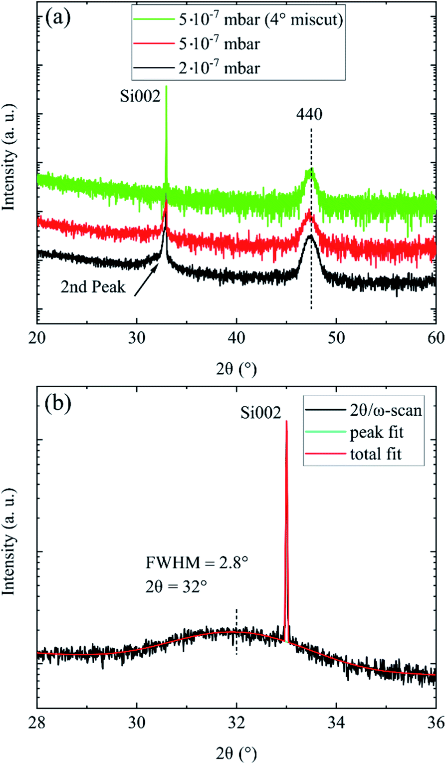 | ||
| Fig. 5 (a) Symmetric 2θ/ω measurements of the Gd2O3 layers grown at pO2 = 2·10−7 mbar, pO2 = 5·10−7 mbar and pO2 = 5·10−7 mbar and 4° miscut Si substrates with a nominal thickness of around 10 nm. (b) Symmetric 2θ/ω measurements of the Gd2O3 layers grown at pO2 = 2·10−7 mbar with a higher signal to noise ratio. | ||
The maximum of this reflection reveals to 2θ ≈ 32° with a full width at half maximum (FWHM) of 2.8°, which was approximated with a Gaussian function. This reflection cannot be attributed to the phenomenon “Umweganregung”.47 Two possible explanations for the appearance of this peak could be applied: (1) the growth of Gd2O3 in (100) orientation and a tetragonal distortion of the crystal lattice or (2) the formation of a tetragonal phase. The peak position of the (400) reflection reveals to 2θ ≈ 33°, which is around 1° shifted compared to the measured reflection. A tetragonal phase was only reported for another stoichiometry for gadolinium oxide GdO2, which is usually not stable.48 A comparison with crystallographic data from literature49 for tetragonal GdO2 and the use of the program Vesta shows that the reflection could be attributed to the (110) orientation of the structure. This would mean that parts of tetragonal GdO2 with a (110) orientation co-exist with the Gd2O3 layer. The same orientation of both structures could be a further verification of the hypothesis. The origin of this peak will be further discussed later in the chapter.
For a further investigation of the crystal structure, the Gd2O3 layers were investigated using grazing incidence XRD (GIXRD) with ϕ-scans. The Gd2O3 layer grown at pO2 = 5·10−7 mbar was aligned on the 400 reflection of the (110) oriented layer in [110] in-plane direction of the substrate. After that, the ϕ angle was varied while the intensity was detected. The measurement (Fig. 6a) shows sharp reflections at a distance of 90°, which indicates a fourfold symmetry of the layer. However, the (110) orientation should only exhibit a twofold symmetry. Therefore, it can be suggested that the layer consists of two (110) domains orthogonal oriented in-plane, as also suggested from RHEED investigations. The two small peaks in between at a distance of 45° could arise from the in-plane net planes of the suggested tetragonal phase or tetragonal distorted cubic structure with (100) orientation.
 | ||
| Fig. 6 (a) φ-Scan in GIXRD geometry of the (400) reflection of the Gd2O3 layer grown at pO2 = 5·10−7 mbar and (b) φ-scan of the asymmetric 222 reflection of the Gd2O3 layer grown at pO2 = 5·10−7 mbar on a 4° miscut substrate. | ||
The ϕ-scan of the Gd2O3 layer grown on the 4° miscut substrate (Fig. 6b) was performed at the asymmetric 222 reflection of the layer. It shows reflections at a distance of 90°, which also indicates the growth in two orthogonal domains. However, the peaks appearing at a distance of 180° have high intensity, wherefore the reflection at a distance of 90° apart from these exhibits a much lower intensity. This behaviour can be interpreted that the amount of one domain in the layer is smaller than the other. The orientation of the domains with respect to the silicon substrate can be found elsewhere.20
The surface morphology of the Gd2O3 layers was also investigated with AFM and is depicted in Fig. 7. On the surface of the Gd2O3 layer grown at pO2 = 2·10−7 mbar nanowire-like structures can be seen similar to the structures observed for thinner layers. The nanowire-like structures are also arranged orthogonal to each other along with the equivalent [110] directions of the substrate, in accordance with the GIXRD measurements. The AFM image of the Gd2O3 layer grown at pO2 = 5·10−7 mbar shows almost the same nanowire-like structure but with a smaller length and higher density. This might be due to the lower mobility of the adatoms in the presence of a larger amount of oxygen atoms on the surface. The average height of the structures is around 4–5 nm, which is depicted in a line scan of the surface (Fig. 7d), where the side walls might be inclined. The AFM image of the Gd2O3 layer grown on the 4° miscut substrate (Fig. 7c) also shows nanowire-like structures, but with mainly single orientation (orthogonal to the wafer flat in one [110] direction) in accordance to the XRD measurements. The height of the nanowire-like structures and inclined sidewalls compares to that found for the structures grown on well-oriented samples (Fig. 7e).
 | ||
| Fig. 7 AFM images of the Gd2O3 layers grown at (a) pO2 = 2·10−7 mbar (b) pO2 = 5·10−7 mbar and (c) pO2 = 5·10−7 mbar on a 4° miscut substrate. (d) Line profile of the layers from (a) and (e) line profile of the layer from (c). | ||
For a further evaluation of the observed structures, SEM images of the surface of the Gd2O3 grown at pO2 = 2·10−7 mbar and pO2 = 5·10−7 mbar (Fig. 8) were obtained. The surface of the Gd2O3 exhibits almost identical structures compare to the AFM images, wherefore a noise or AFM tip effect on the AFM images can be ruled out.
 | ||
| Fig. 8 SEM images of the Gd2O3 grown at high temperatures and higher nominal thickness. (a) Gd2O3 grown at pO2 = 2·10−7 mbar and (b) pO2 = 5·10−7 mbar. | ||
Furthermore, the Gd2O3 layers were investigated by TEM in a cross-section view, which is depicted in Fig. 9. In the TEM image of the layer grown at pO2 = 2·10−7 mbar no sharp interface between the layer and the substrate can be seen (Fig. 9a). Furthermore, the TEM images show irregular faceting of the silicon surface with a certain orientation, as already suggested from RHEED and AFM investigations. The orientation of the formed facets can be determined through the measurement of the angle in relation to the original surface of the silicon and measures to around φ1 = 50°–60°. In this range, the angle between the (001) and (110) net planes of the cubic structure is located, which reveals to φ = 54.74°. These observations lead to the assumption, that the facets in the Si surface exhibit a (111) orientation. In general, it is known that for Si the surface energy of the (111) orientation is the lowest in comparison to the (110) and (001) orientation.50,51 Therefore, the formation of such facets is likely.
 | ||
| Fig. 9 TEM images of the Gd2O3 layers grown at (a) pO2 = 2·10−7 mbar and (b) pO2 = 5·10−7 mbar. Some domain boundaries are marked with white lines. The angles φ1 and φ2 describe the angles between the orientation of the facetted silicon and Gd2O3 surface, as described in the main text. | ||
On this facetted surface, almost uniform coverage of the surface with a layer with darker contrast as the substrate and a regular arrangement of atomic rows can be seen, which indicates a well-crystallized structure of the Gd2O3 layer. From the top edges of the trenches in the silicon surface and the deepest points of the trenches, domain boundaries originate, which are marked with white lines (Fig. 9a). The surface of the Gd2O3 layer shows also faceting. The XRD investigations have shown that the Gd2O3 layer consists almost only of the cubic structure with (110) orientation parallel with the Si(001) surface normal. The angle φ2 between the facets and the (110) orientation of the layer can be estimated to be in the range of 30°–40° (Fig. 9a). In this range, the angle between the (110) and (111) orientation to φ = 35.26° can be found, which is also an indication for the formation of {111} facets. This behaviour follows the Wulff theorem, where the direction with lower surface energy (111) has a lower growth speed than the (110) direction.52 Therefore, the (110) facets with higher surface energy vanish.
It is interesting to note, that on the {111}-facetted sidewalls of the Si trenches in the Si surface nearly perfect growth of Gd2O3 in (111) orientation occurs. That agrees with results for the growth of Gd2O3 on Si(111).19 In such a case, the (100) net planes of the Gd2O3 layer are oriented parallel to the (001) substrate orientation and XRD investigation of the out-of-plane net planes should show a (400) reflection. There might be a correlation with the suggested (100) orientation, which was assumed from the previous XRD investigation. The growth of the Gd2O3 on the facetted Si surface is depicted in Fig. 10 with a schematic drawing, where the orientation of the Gd2O3 is shown for the different regions.
 | ||
| Fig. 10 Schematic drawing of the different growth regions on the facetted silicon surface. (a) Regions of Gd2O3 growth on the Si(001) surface (b) regions of Gd2O3 growth on {111} facetted Si surface. | ||
At some parts of the interface between the layer and the substrate a thin interfacial layer with irregular contrast can be seen, which indicates an amorphous structure. For the growth of Gd2O3 on Si(001) the formation of a thin amorphous interfacial layer is already known.53 The Gd2O3 layer grown at pO2 = 5·10−7 mbar show similar TEM images (Fig. 9b), however, the quasi-amorphous layer has nearly vanished.
Moreover, on the one hand, the faceting of the silicon surface is an indication for a strong rearrangement within the surface. On the other hand, the silicon could react with the gadolinium to a silicide. The formation of volatile SiO could also be possible as an accompanying process. This will be discussed in the next section.
Discussion
The formation of nanowires, nanowire-like structures and islands are well-known for metal silicides grown on silicon surfaces.54–59 But the formation of nanowire-like structures during the growth of REOs on Si(001) consisting of oxides was not reported so far.In the following, the formation of the nanowire-like structures of Gd2O3 during epitaxial growth at high temperatures will be discussed in terms of thermodynamic and kinetic processes.
The nanowire-like structures are oriented in two different directions along with the [110] directions of the substrate. The dimer rows of the (2 × 1) reconstruction on the Si(001) surface are also oriented along the [110] direction and therefore oriented orthogonal to the neighboring terraces, which are separated by monoatomic steps. The [110] direction is also the direction with a smaller misfit between Si and Gd2O3, which could lead to the elongation of the nanowire-like structures in [110] direction, instead of growing in the [100] direction with a higher misfit. Furthermore, the diffusion barrier parallel to the dimer rows is smaller compare to orthogonal.60 Therefore, gadolinium monoxide (GdO), which is the predominant species during the electron beam evaporation,61 will predominantly diffuse parallel to the dimer rows and attach to the surface. The originating islands will further elongate to the nanowire-like structures. An increase in oxygen partial pressure leads to a decrease in surface diffusion length due to a higher density of adatoms on the surface. Hence, a higher amount of nanowire-like structures with smaller lengths will form. The Gd2O3 layer grown on a 4° miscut sample shows only one preferential orientation of the nanowire-like structures in the AFM investigations. At temperatures in the range of 875 °C, it is known that on miscut substrates double atomic steps can be formed.62–64 If double atomic steps are present on the silicon surface, the dimer rows on all terraces have the same orientation and the approaching adatoms will preferentially diffuse along with the dimer orientation. The growth temperature in this work is 850 °C and therefore, the formation of a significant amount of double steps can be expected. This assumption also matches with the observation from symmetric investigations with XRD and AFM, which indicates the dominance of only one domain.
For the growth of CaF2 on Si(001) similar structures were found.65 Pasquali et al. reported on the formation of nanowires during the growth of CaF2 at higher temperatures on Si(001) oriented along with the [110] direction for submonolayer coverage of the surface.65,66 Loretto et al. also reported on quasi-one-dimensional CaF2 islands on Si(001), which are even more similar to the structure in this work.67 The one-dimensional CaF2 islands were also oriented along with the [110] direction of the Si(001) surface and exhibit a width of a few nanometers and a length of some micrometers. Moreover, they show a faceting of the surface with {111} facets, which is equivalent to the Gd2O3 structures in this work.
The faceting of nanowires was also reported for CeO2 grown on α-Al2O3 substrates, where also predominantly {111} facets on elongated islands or nanowires are formed.68 This is not surprising since the (111) surface of the REOs is energetically the most favourable.69,70
Faceting of the surface can occur when mass transport is sufficient to allow a change in orientation and could be achieved at high surface diffusion.71 At growth temperatures in the range of 850 °C a high surface diffusion length of the adatoms can be expected, which could be the reason for the faceting. Furthermore, the faceting of the silicon surface indicates a rearrangement of the surface before or during the growth of the oxide. For this process different mechanisms could be taken into account: (1) the formation of a silicide through the reaction with silicon, (2) a self-organized rearrangement of the silicon surface for energy minimization and (3) a reaction of silicon with oxygen and the formation of SiO and subsequent desorption.
The formation of a silicide (GdSix) or an oxide (Gd2O3) on silicon surface during the impinging of GdO molecular fragments depends on the chemical potential of oxygen on the Si surface. For the system praseodym and oxygen on Si(001) different compounds ranging from silicides to oxides were found in dependence of the oxygen chemical potential.72 It has been shown, that a silicide formation at the lower oxygen chemical potential is favoured. For the growth of Gd2O3 on Si(001) at 600 °C and pO2 = 5·10−7 mbar no silicide formation was observed.53 However, since the oxygen chemical potential decreases significantly with an increase in temperature and constant oxygen partial pressure,73 it could be possible that due to an increase in temperature the silicide formation is favoured over oxide formation. The same effect could appear for a decrease in oxygen partial pressure at constant T, as reported for the initial stage of growth of Nd2O3 on Si(001) at low oxygen partial pressure.18
The silicide is then transformed to Gd2O3 during further growth at a nominal thickness of >1 nm. No silicide formation was found for a nominal thickness of 2 nm in the XRD investigation. This is supported by the results of TEM studies, where a layer system consisting of two stacked crystalline layers, a silicide layer coexisting with an oxide layer, was not observed. The RHEED pattern in the initial stage of the growth shows a change with increasing thickness, which can be interpreted in terms of change in the crystalline surface structure. However, the typical (3 × 1) reconstruction for a silicide-like surface structure has not been observed, indicating that this surface structure is not stable at high temperatures.74 At a thickness of around 2 nm, the RHEED pattern is rather similar to the pattern observed for Gd2O3 layers with higher nominal thickness and could therefore be attributed to the cubic Gd2O3 with (110) orientation.
Furthermore, for rare-earth silicides there is a high tendency for nanowire-like structure formation on Si surfaces.57,58,75,76 Eames et al. show in calculations, that a growth of the silicide nanowires along the dimer rows is energetically favourable.77 The rare-earth silicide nanowires grown on Si(001) are usually arranged along with the [110] directions of the Si(001) surface57,58,75,76 and have a similar shape, as the nanowire-like structures observed in this study. This supports the assumption of a silicide formation in the initial stage of growth and suggests that Gd2O3 nanowire formation is initiated through this. Furthermore, during the growth on vicinal surfaces, the rare-earth silicide nanowires align only along with one [110] direction,59,78,79 which is also similar to the observation in this work. For the explanation of this behaviour, the formation of double steps is also discussed.
Investigations on the growth of silicides on Si(001) due to deposition of other metals, like manganese, titanium or nickel, show a similar behaviour compared to the structures in this work.80 For example, during the growth of manganese, elongated silicide structures are forming on the silicon surface, which are oriented orthogonal along with the [110] directions. During the growth of titanium silicide, so-called erosion structures are forming on the silicon surface, which is explained due to a high silicon migration from the substrate. This is accompanied by a strong vacancy formation on the surface, which results in the formation of pyramid-like structures on the surface.80 Furthermore, for the growth on Si(001), nickel silicide islands are growing into the silicon substrate, whereby {111} facets are forming predominantly.81 This behaviour is attributed to higher nickel diffusion into the substrate. Because of the usage of these high growth temperatures in this work high surface mobility of the Si and Gd atoms can be assumed and can be taken as a reason for the formation of such structures.
Summarizing, the layer formation process could be described as follows. First, a silicide layer is formed during the impingement of the Gd atoms and GdO molecular fragments on the surface, which forms nanowire-like structures. These structures grow until a critical thickness, where the transformation to oxide occurs and further growth in the oxide structure. This is accompanied by a strong faceting of the Si(001) surface. In the literature, there are reports about the transformation of a silicide in contact with oxygen into an oxide.82,83 The layer formation process is depicted schematically in Fig. 11.
 | ||
| Fig. 11 Schematic drawing of (a) the silicide formation with erosion structures (adapted from ref. 80) and (b) the transformation into oxide and further growth. The black squares represent the Gd atoms, the grey circles represent the Si atoms and the red circles represent the O atoms. | ||
During the transformation of the silicide into an oxide, the silicon from the silicide has to react to a gaseous product. One possibility could be the reaction to gaseous SiO. Moreover, the reaction of oxygen and silicon could already have been triggered before the silicide formation. During the contact of silicon with oxygen, it depends on the temperature and the oxygen partial pressure whether a layer of SiO2 or gaseous SiO [eqn (1)] is formed. The chosen conditions of 850 °C and pO2 = 5·10−7 mbar are in the range where the reaction to SiO can be expected.84 This reaction leads to etching of silicon.
| 2Si(s) + O2(g) → 2SiO(g) | (1) |
During such an etching process always the Si surfaces with the lowest surface energy will form, which is the (111) surface.50,51 In the TEM images {111} faceting of the Si surface was indeed observed (Fig. 9), which is consistent with earlier studies.85
Furthermore, in some cases, small islands can be seen between the nanowire-like structures (Fig. 12). These islands exhibit a height up to 20 nm and are surrounded by trenches. Mogilatenko et al. reported about similar structures during the formation of manganese silicide and nickel silicide.81 The growth has been described by a model,86 which could also be applied for gadolinium silicide.
 | ||
| Fig. 12 (a) and (b) AFM images of Gd2O3 layers grown at pO2 = 5·10−7 mbar with different nominal thickness. In both images, small islands with a height up to 20 nm can be seen. | ||
During the impinging of the molecular fragments of Gd2O3 on the silicon surface, they have high surface mobility. If they reach a step edge or defects, the reaction to form a silicide can start.86 The formation of silicide islands demands the consumption of silicon from the substrate, which will be taken from the surrounded areas, wherefore the trenches can form. This is also the case for the nanowire-like structures.
Fig. 13 illustrates the formation process of the silicide islands. The very large height of the islands and the low depth of the trenches indicate, that also silicon from a further distance takes part in the island formation. Therefore, high surface mobility of Si is needed, which is the case at high temperatures. TEM investigations also indicate the consumption of silicon originating from more distant parts of the island surroundings. Similar structures were found during the annealing of silicon on insulator (SOI) structures consisting of silicon and Gd2O3.87 Moreover, Miccoli et al. reported on the formation of silicide islands during the epitaxial growth of terbium silicide nanowires.59
 | ||
| Fig. 13 Schematic drawing of the model for the formation of the silicide islands during the growth of Gd2O3 on Si(001) at 850 °C. The empty circles represent the silicon atoms and the filled circles represent the gadolinium atoms. Adapted from ref. 86. | ||
Conclusions
In this work, we studied the structural and morphological properties of Gd2O3 grown with molecular beam epitaxy on Si(001) at high temperatures (850 °C). Especially, we investigated the influence of oxygen partial pressure and a substrate miscut on the growth mechanism as well as the layer formation during different stages of growth.During the initial stage of growth of Gd2O3 on Si(001), the surface starts to roughen. This is very likely initiated by silicide formation. Subsequently, the silicide transforms into oxide during further growth. The Gd2O3 grows in nanowire-like structures oriented parallel along the Si dimer rows of the initial (2 × 1) reconstructed Si(001) surface. The sidewalls of the nanowire-like structures are (111) planes, where Gd2O3 grow nearly perfect epitaxially. Furthermore, the number and size of the nanowire-like structures can be modified by varying the oxygen partial pressure, where the density and length of the structures are higher for higher oxygen partial pressure due to the lower surface mobility of the adatoms, whereas their length becomes smaller. Moreover, the orientation of the nanowire-like structures can be influence by growing on a sample with 4° miscut.
The initial formation process of the nanowire-like structures could be explained by surface kinetics and thermodynamics of phase formation, where the adatoms diffuse predominantly along the dimer rows of the (2 × 1) reconstruction attach to the surface and form the nanowire-like structures. It can be suggested, that the silicide formation is an essential part of the formation of the nanowire-like structures. Moreover, small islands form simultaneously to the nanowire-like structures, which is also attributed to silicide formation.
In this way, we showed how to modify the morphology of the Gd2O3 grown on Si(001) by varying the growth parameters during molecular beam epitaxy and adapted suitable models to explain the growth behaviour. This could open the way to synthesize shape-controlled rare earth oxide nanostructures on Si for integration into the established Si-technology.
Conflicts of interest
There are no conflicts to declare.Acknowledgements
P. Gribisch would like to acknowledge the Minna-James-Heineman foundation for a scholarship. We further like to thank the Laboratory of Nano and Quantum Engineering (LNQE) for the access to the TEM facility and Andrea Lissel for the TEM sample preparation. Furthermore, we would like to thank Okan Samast for the help with some investigations. We thank Steffen Börnert for conducting some AFM images. The SEM images were conducted at the IIT Bombay in cooperation with the group of Apurba Laha. The publication of this article was funded by the Open Access Fund of the Leibniz Universität Hannover.References
- G. Charalampides, K. I. Vatalis, B. Apostoplos and B. Ploutarch-Nikolas, Procedia Econ. Financ., 2015, 24, 126–135 CrossRef.
- R. G. Wang, V. Sama, D. Q. Li and S. I. Mutinda, Adv. Mater. Res., 2012, 512–515, 1624–1629 CAS.
- R. Weber, J. A. Tangeman, P. C. Nordine, R. N. Scheunemann, K. J. Hiera and C. S. Ray, J. Non-Cryst. Solids, 2004, 345–346, 359–365 CrossRef.
- T. Tanaka, M. Kuzuhara, M. Watada and M. Oshitani, J. Alloys Compd., 2006, 408–412, 323–326 CrossRef CAS.
- G. Azimi, R. Dhiman, H.-M. Kwon, A. T. Paxson and K. K. Varanasi, Nat. Mater., 2013, 12, 315–320 CrossRef CAS.
- F. Druon, M. Velázquez, P. Veber, S. Janicot, O. Viraphong, G. Buşe, M. A. Ahmed, T. Graf, D. Rytz and P. Georges, Opt. Lett., 2013, 38, 4146–4149 CrossRef CAS PubMed.
- H. Rétot, A. Bessière, B. Viana and A. Galtayries, J. Appl. Phys., 2011, 109, 123518 CrossRef.
- H. D. B. Gottlob, T. Echtermeyer, T. Mollenhauer, J. K. Efavi, M. Schmidt, T. Wahlbrink, M. C. Lemme, H. Kurz, M. Czernohorsky, E. Bugiel, H.-J. Osten and A. Fissel, Solid-State Electron., 2006, 50, 979–985 CrossRef CAS.
- R. Sarkar, S. Bhunia, D. Nag, B. C. Barik, K. Das Gupta, D. Saha, S. Ganguly, A. Laha, J. Lemettinen, C. Kauppinen, I. Kim, S. Suihkonen, P. Gribisch and H.-J. Osten, Appl. Phys. Lett., 2019, 115, 63502 CrossRef.
- K. J. Hubbard and D. G. Schlom, J. Mater. Res., 1996, 11, 2757–2776 CrossRef CAS.
- J. Robertson, Rep. Prog. Phys., 2006, 69, 327–396 CrossRef CAS.
- H. J. Osten, D. Kühne, A. Laha, M. Czernohorsky, E. Bugiel and A. Fissel, J. Vac. Sci. Technol. B, 2007, 25, 1039 CrossRef CAS.
- A. Fissel, H. J. Osten and E. Bugiel, J. Vac. Sci. Technol. B, 2003, 21, 1765 CrossRef CAS.
- T. Inoue, T. Ohsuna, L. Luo, X. D. Wu, C. J. Maggiore, Y. Yamamoto, Y. Sakurai and J. H. Chang, Appl. Phys. Lett., 1991, 59, 3604–3606 CrossRef CAS.
- K. Tachi, H. Iwai, T. Hattori, N. Sugii, K. Tsutsui, P. Ahemt and K. Kakushima, ECS Trans., 2006, 3, 425–434 CrossRef CAS.
- H. Yang, H. Wang, H. M. Luo, D. M. Feldmann, P. C. Dowden, R. F. DePaula and Q. X. Jia, Appl. Phys. Lett., 2008, 92, 62905 CrossRef.
- H. Osten, J. Liu, E. Bugiel, H. Müssig and P. Zaumseil, J. Cryst. Growth, 2002, 235, 229–234 CrossRef CAS.
- A. Fissel, Z. Elassar, O. Kirfel, E. Bugiel, M. Czernohorsky and H. J. Osten, J. Appl. Phys., 2006, 99, 074105 CrossRef.
- H. J. Osten, A. Laha, M. Czernohorsky, E. Bugiel, R. Dargis and A. Fissel, Phys. Status Solidi A, 2008, 205, 695–707 CrossRef CAS.
- P. Gribisch, J. Schmidt, H.-J. Osten and A. Fissel, Acta Cryst. B, 2019, 75, 59–70 CrossRef CAS PubMed.
- J. Wang, A. Laha, A. Fissel, D. Schwendt, R. Dargis, T. Watahiki, R. Shayduk, W. Braun, T. Liu and H. J. Osten, in 2009 4th IEEE International Conference on Nano/Micro Engineered and Molecular Systems, IEEE, 2009, pp. 436–440 Search PubMed.
- D. Schwendt, H. J. Osten, P. Shekhter and M. Eizenberg, Appl. Phys. Lett., 2012, 100, 232905 CrossRef.
- G. A. Hussein, J. Anal. Appl. Pyrolysis, 1996, 37, 111–149 CrossRef CAS.
- X.-P. Fu, L.-W. Guo, W.-W. Wang, C. Ma, C.-J. Jia, K. Wu, R. Si, L.-D. Sun and C.-H. Yan, J. Am. Chem. Soc., 2019, 141, 4613–4623 CrossRef CAS PubMed.
- X. Yang, X. Cheng, J. Ma, Y. Zou, W. Luo and Y. Deng, Small, 2019, 15, 1903058 CrossRef.
- J. D. Lessard, I. Valsamakis and M. Flytzani-Stephanopoulos, Chem. Commun., 2012, 48, 4857–4859 RSC.
- W. Gao, Z. Zhang, J. Li, Y. Ma and Y. Qu, Nanoscale, 2015, 7, 11686–11691 RSC.
- M. Flytzani-Stephanopoulos, M. Sakbodin and Z. Wang, Science, 2006, 312, 1508–1510 CrossRef CAS PubMed.
- R. Li, S. Yabe, M. Yamashita, S. Momose, S. Yoshida, S. Yin and T. Sato, Solid State Ionics, 2002, 151, 235–241 CrossRef CAS.
- Y. D. Jiang, Z. L. Wang, F. Zhang, H. G. Paris and C. J. Summers, J. Mater. Res., 1998, 13, 2950–2955 CrossRef CAS.
- Y. Kadowaki and K. Aika, J. Catal., 1996, 161, 178–185 CrossRef CAS.
- R. S. Meltzer, S. P. Feofilov, B. Tissue and H. B. Yuan, Phys. Rev. B, 1999, 60, R14012–R14015 CrossRef CAS.
- K. Kömpe, H. Borchert, J. Storz, A. Lobo, S. Adam, T. Möller and M. Haase, Angew. Chem., Int. Ed., 2003, 42, 5513–5516 CrossRef.
- J. W. Stouwdam and F. C. J. M. van Veggel, Nano Lett., 2002, 2, 733–737 CrossRef CAS.
- M. Yada, H. Kitamura, A. Ichinose, M. Machida and T. Kijima, Angew. Chem., Int. Ed., 1999, 38, 3506–3510 CrossRef CAS PubMed.
- K. Yuan and Y.-W. Zhang, Inorg. Chem. Front., 2020, 7, 4256–4280 RSC.
- H.-P. Zhou, Y.-W. Zhang, H.-X. Mai, X. Sun, Q. Liu, W.-G. Song and C.-H. Yan, Chem.–Eur. J., 2008, 14, 3380–3390 CrossRef CAS PubMed.
- R. Si, Y.-W. Zhang, H.-P. Zhou, L.-D. Sun and C.-H. Yan, Chem. Mater., 2007, 19, 18–27 CrossRef CAS.
- R. Si, Y.-W. Zhang, L.-P. You and C.-H. Yan, Angew. Chem., Int. Ed., 2005, 44, 3256–3260 CrossRef CAS.
- H.-X. Mai, L.-D. Sun, Y.-W. Zhang, R. Si, W. Feng, H.-P. Zhang, H.-C. Liu and C.-H. Yan, J. Phys. Chem. B, 2005, 109, 24380–24385 CrossRef CAS.
- A. Ichimiya and P. I. Cohen, Reflection high-energy electron diffraction, Cambridge University Press, 2004 Search PubMed.
- P. R. Pukite, S. Batra and P. I. Cohen, in Growth of Compound Semiconductors, ed. R. L. Gunshor and H. Morkoc, SPIE, 1987, pp. 22–26 Search PubMed.
- G. Woltersdorf and B. Heinrich, Phys. Rev. B, 2004, 69, 184417 CrossRef.
- P. Villars and K. Cenzual, GdSi2-x (GdSi2 ht hex) Crystal Structure: Datasheet from PAULING FILE Multinaries Edition - 2012” in SpringerMaterials, Springer Verlag, Berlin Heidelberg, 2012, https://materials.springer.com/isp/crystallographic/docs/sd_0450688 Search PubMed.
- P. Villars and K. Cenzual, GdSi2 Crystal Structure: Datasheet from “PAULING FILE Multinaries Edition - 2012” in SpringerMaterials, Springer Verlag, Berlin Heidelberg, 2012, https://materials.springer.com/isp/crystallographic/docs/sd_0530825 Search PubMed.
- K. Momma and F. Izumi, J. Appl. Crystallogr., 2011, 44, 1272–1276 CrossRef CAS.
- P. Zaumseil, J. Appl. Crystallogr., 2015, 48, 528–532 CrossRef CAS PubMed.
- S. A. Semiletov, R. M. Imamov, N. A. Ragimli and L. I. Man, Thin Solid Films, 1976, 32, 325–328 CrossRef CAS.
- P. Villars and K. Cenzual, GdO2 Crystal Structure: Datasheet from “PAULING FILE Multinaries Edition - 2012” in SpringerMaterials, Springer Verlag, Berlin Heidelberg, 2012, https://materials.springer.com/isp/crystallographic/docs/sd_1602110 Search PubMed.
- J. J. Gilman, J. Appl. Phys., 1960, 31, 2208–2218 CrossRef CAS.
- R. J. Jaccodine, J. Electrochem. Soc., 1963, 110, 524 CrossRef CAS.
- G. Wulff, Z. für Kristallogr.–Cryst. Mater., 1901, 34, 449–530 CrossRef CAS.
- M. Czernohorsky, E. Bugiel, H. J. Osten, A. Fissel and O. Kirfel, Appl. Phys. Lett., 2006, 88, 152905 CrossRef.
- Y. Chen, D. A. A. Ohlberg, G. Medeiros-Ribeiro, Y. A. Chang and R. S. Williams, Appl. Phys. Lett., 2000, 76, 4004–4006 CrossRef CAS.
- Y. Chen, D. A. Ohlberg and R. Stanley Williams, Mater. Sci. Eng. B, 2001, 87, 222–226 CrossRef.
- Y. Chen, D. A. A. Ohlberg and R. S. Williams, J. Appl. Phys., 2002, 91, 3213–3218 CrossRef CAS.
- J. Nogami, B. Z. Liu, M. V. Katkov, C. Ohbuchi and N. O. Birge, Phys. Rev. B, 2001, 63, 233305 CrossRef.
- G. Ye, M. A. Crimp and J. Nogami, J. Appl. Phys., 2009, 105, 104304 CrossRef.
- I. Miccoli, F. Edler, H. Pfnür, S. Appelfeller, M. Dähne, K. Holtgrewe, S. Sanna, W. G. Schmidt and C. Tegenkamp, Phys. Rev. B, 2016, 93, 125412 CrossRef.
- D. Srivastava and B. J. Garrison, Phys. Rev. B., 1992, 46, 1472–1479 CrossRef CAS PubMed.
- L. L. Ames, P. N. Walsh and D. White, J. Phys. Chem., 1967, 71, 2707–2718 CrossRef CAS.
- R. Kaplan, Surf. Sci., 1980, 93, 145–158 CrossRef CAS.
- P. E. Wierenga, J. A. Kubby and J. E. Griffith, Phys. Rev. Lett., 1987, 59, 2169–2172 CrossRef CAS PubMed.
- A. Laha, E. Bugiel, J. X. Wang, Q. Q. Sun, A. Fissel and H. J. Osten, Appl. Phys. Lett., 2008, 93, 182907 CrossRef.
- L. Pasquali, S. D'Addato, G. Selvaggi, S. Nannarone, N. S. Sokolov, S. M. Suturin and H. Zogg, Nanotechnology, 2001, 12, 403–408 CrossRef CAS.
- L. Pasquali, S. M. Suturin, V. P. Ulin, N. S. Sokolov, G. Selvaggi, A. Giglia, N. Mahne, M. Pedio and S. Nannarone, Phys. Rev. B, 2005, 72, 45448 CrossRef.
- D. Loretto, F. M. Ross and C. A. Lucas, Appl. Phys. Lett., 1996, 68, 2363–2365 CrossRef CAS.
- S. N. Jacobsen, U. Helmersson, R. Erlandsson, B. Skårman and L. R. Wallenberg, Surf. Sci., 1999, 429, 22–33 CrossRef CAS.
- M. Nolan, S. Grigoleit, D. C. Sayle, S. C. Parker and G. W. Watson, Surf. Sci., 2005, 576, 217–229 CrossRef CAS.
- J. Tam, B. Feng, Y. Ikuhara, H. Ohta and U. Erb, J. Mater. Chem. A, 2018, 6, 18384–18388 RSC.
- E. D. Williams and N. C. Bartelt, Ultramicroscopy, 1989, 31, 36–48 CrossRef.
- J. Dąbrowski and V. Zavodinsky, Ab Initio Study of Pr Oxides for CMOS Technology, NIC Symposium 2004, Proceedings, 2004, pp. 171–180 Search PubMed.
- J. Rogal and K. Reuter, Ab Initio Atomistic Thermodynamics for Surfaces: A Primer, Defense Technical Information Center, 2006 Search PubMed.
- A. Roy Chaudhuri, A. Fissel and H. J. Osten, Appl. Phys. Lett., 2014, 104, 12906 CrossRef.
- S. K. Song, T.-H. Kim and H. W. Yeom, Sci. Rep., 2019, 9, 1364 CrossRef PubMed.
- S. Li, H. Cai, C. L. Gan, J. Guo and J. Ma, J. Mater. Chem., 2012, 22, 20958 RSC.
- C. Eames, M. I. J. Probert and S. P. Tear, Appl. Phys. Lett., 2010, 96, 241903 CrossRef.
- B. Z. Liu and J. Nogami, Nanotechnology, 2003, 14, 873–877 CrossRef CAS.
- E. P. Rugeramigabo, C. Tegenkamp, H. Pfnür, T. Inaoka and T. Nagao, Phys. Rev. B, 2010, 81, 165407 CrossRef.
- H. Hortenbach, Doctoral thesis, Technische Universität Chemnitz, 2003.
- A. Mogilatenko, M. Falke, H. Hortenbach, S. Teichert, G. Beddies and H.-J. Hinneberg, J. Cryst. Growth, 2005, 283, 303–308 CrossRef CAS.
- F. M. d'Heurle, A. Cros, R. D. Frampton and E. A. Irene, Philos. Mag. B, 1987, 55, 291–308 Search PubMed.
- R. Mitra, Diffus. Found., 2019, 21, 127–156 CAS.
- F. W. Smith and G. Ghidini, J. Electrochem. Soc., 1982, 129, 1300 CrossRef CAS.
- T. Engel, Surf. Sci. Rep., 1993, 18, 93–144 CrossRef.
- A. Mogilatenko, M. Falke, H. Hortenbach, S. Teichert, G. Beddies and H.-J. Hinneberg, Appl. Surf. Sci., 2006, 253, 561–565 CrossRef CAS.
- R. Dargis, A. Fissel, D. Schwendt, E. Bugiel, J. Krügener, T. Wietler, A. Laha and H. J. Osten, Vacuum, 2010, 85, 523–526 CrossRef CAS.
| This journal is © The Royal Society of Chemistry 2021 |