 Open Access Article
Au decorated BiVO4 inverse opal for efficient visible light driven water oxidation
Xiaonong Wang *ab,
Xiaoxia Li*ab and
Jingxiang Low
 c
c
aState Key Laboratory of Pulsed Power Laser Technology, College of Electronic Engineering, National University of Defense Technology, Hefei 230037, China. E-mail: wangxiaonong2016@163.com; lxxhong@163.com
bKey Laboratory of Infrared and Low Temperature Plasma of Anhui Province, Hefei 230037, China
cHefei National Laboratory for Physical Sciences at the Microscale, Collaborative Innovation Center of Chemistry for Energy Materials (iChEM), School of Chemistry and Materials Science, National Synchrotron Radiation Laboratory, University of Science and Technology of China, Hefei, Anhui 230026, P. R. China
First published on 25th February 2021
Abstract
Photocatalytic water splitting provides an effective way to prepare hydrogen and oxygen. However, the weak light utilization and sluggish kinetics in the oxygen evolution reaction (OER) process substantially retard the photocatalytic efficiency. In this context, modification of the semiconductors to overcome these limits has been the effective strategy for obtaining highly-efficient photocatalytic water oxidation. Here, plasmonic Au has been loaded onto BiVO4 inverse opal (IO) for photocatalytic water oxidation. It is discovered that the IO structure provides higher specific surface area and favors light absorption on BiVO4. In the meantime, the plasmonic Au can simultaneously enhance the light-utilization capability and photogenerated charge carrier utilization ability of the BiVO4 IO. As a result, a high photocurrent density and long photogenerated charge carrier lifetime can be achieved on the optimized Au–BiVO4 IO, thereby obtaining a superior photocatalytic activity with an oxygen production rate of 9.56 μmol g−1 h−1.
1 Introduction
Over the past century, the development and utilization of solar energy has been one hot topic for tackling the increasingly serious environmental and energy problems due to our dependency on the traditional coal fuel for power generation and supply.1–4 In this regard, solar-driven water splitting, which could directly convert and store the incident solar energy into valuable hydrogen and oxygen, has been one of the star–catalytic reactions toward realizing sustainable and green development of human society.3,5,6 Therefore, in the past several decades, various semiconductors, such as TiO2 and WO3, have been investigated for the photocatalysis.7–9 However, their wide bandgap, rapid electron–hole pair recombination and sluggish kinetics in oxygen evolution reaction have substantially retarded the solar conversion efficiency of such a fascinating technology.Under this circumstance, water oxidation kinetics of the photocatalysts should be optimized and facilitated, accompanying with enhanced light absorption and efficient charge separation to reach highly-efficient photocatalytic water splitting. Recently, BiVO4, a small bandgap (2.4 eV vs. reversible hydrogen electrode (RHE)) semiconductor with high oxidation ability, has been known as one of potential oxidative semiconductor for the photocatalytic water splitting.10–12 Apart from that, its low cost, high chemical stability and environmental friendliness characteristics have allowed it to be feasible in future large-scale application of photocatalytic water splitting. However, most of the recently reported BiVO4 owns low photocurrent densities mainly due to the electrons and holes rapid recombination in the bulk or on the surface and weak light utilization capability, which restricts their wide application in photocatalytic water splitting.13–16 With these limitations in mind, many effective approaches have been explored, such as morphology control (nano dots, nano leaves),17,18 crystal-surface engineering19 and homo/heterojunction constructing (type II and S scheme heterojunction).8,9,14–16
Fabrication of the BiVO4 into various morphology with the specific functions has been a simple yet effective strategy for enhancing its physicochemical, especially optical properties.20 For example, Chen et al. reported that the BiVO4 nanoarray structure can endow the BiVO4 with enormous surface active site and enhanced light absorption capability, thereby improving its photocatalytic performance.21 In addition, Ozbay et al. introduced the deposition of Au on BiVO4 nanoarray for enhanced light absorption and high photocurrent generation through the injection of sub-band-gap hot electrons.22 Recently, the inverse opal structure has emerged as a unique morphology for BiVO4 because it can provide a wide variety of porous structure for the catalytic reaction and allow the multi-scattering of light within its structure for enhancing the light utilization capability of the BiVO4.23,24 Apart from the enhanced light utilization capability, the photogenerated charge carrier separation is another critical issues awaiting to be resolved. Constructing heterostructures by combining noble metal crystal with semiconductor can be a potential answer for this problem, due to their higher work function than most of the semiconductors for accepting photogenerated electrons from semiconductors and thus enhancing the photogenerated charge carrier separation efficiency.25–29 In addition, plasmonic noble metals, such as Ag and Au, possess unique surface plasmon resonance (SPR) properties, allowing them to simultaneously facilitate the photogenerated charge carrier separation efficiency and provide SPR-induced “hot electron” for the photocatalytic reaction.28,30–32 The surface plasmon may improve the photocatalytic activities via local electromagnetic field enhancement and resonant energy transfer (RET) mechanisms.33 Due to the strong local field enhancement, the optical absorption can be adjusted and the spatial distribution of photogenerated electron–hole pairs in semiconductors could be modulated.34 And the metal nanoparticle could also serve as the light capture center, enhancing the photo-electric conversion efficiency. More interestingly, RET process could enhance carrier creation and separation at the energies both above and below the bandgap by surface plasmon dipoles relaxation.33 By tuning the plasmonic resonant frequency of Au consistent with BiVO4, the Au surface plasmon resonant energy could directly excite the electrons–holes separation through the near-field electromagnetic interaction. In this work, we report plasmonic Au loaded on BiVO4 inverse opals (Au–BiVO4 IO) for the photocatalytic water oxidation. Generally, Au–BiVO4 IO was prepared by a template-assisted self-assemble method, followed by electron-beam evaporation. Then, the photocatalytic water oxidation of the Au–BiVO4 IO was studied via a photoelectrochemical system under visible light irradiation. Benefiting from the unique features of the IO structure and plasmonic Au, the photocatalytic water oxidation performance of the Au–BiVO4 IO was higher than that of the BiVO4 IO. Apart from that, the photocatalytic enhancement mechanism of the plasmonic Au/BiVO4 IO photocatalyst was proposed and discussed. Such a facile template assisted self-assembly strategy combined with micro-nano fabrication methods for preparation of advanced photocatalyst can shed some light in development of highly efficient visible-light-driven photocatalyst for energy and environmental applications.
2 Experiment procedure
2.1 Chemicals
100 nm, 200 nm and 500 nm monodispersed polystyrene (PS) nanosphere suspensions (2.5 wt% in water, surfactant free) were obtained from Geese (Tianjin) Technology Co., Ltd. Bi(NO3)3·5H2O. NH4VO3, ammonia, nitric acid, hydrogen peroxide, ethanol, acetone and microscopic glass slides were purchased from Sinopharm Chemical Reagent Co., Ltd. The water used in the experiments was deionized. All chemicals were used as received without further purification.![[thin space (1/6-em)]](https://www.rsc.org/images/entities/char_2009.gif) :
:![[thin space (1/6-em)]](https://www.rsc.org/images/entities/char_2009.gif) 7) for 1 h. Then, these glass substrates were washed with DI water for later use. The monodispersed PS nanosphere suspension was diluted by ethanol (1
7) for 1 h. Then, these glass substrates were washed with DI water for later use. The monodispersed PS nanosphere suspension was diluted by ethanol (1![[thin space (1/6-em)]](https://www.rsc.org/images/entities/char_2009.gif) :
:![[thin space (1/6-em)]](https://www.rsc.org/images/entities/char_2009.gif) 2 in volume), and ultrasonicated for fine dispersion. The above-treated glass substrates were inserted into the above-prepared BiVO4 sol, and the PS spheres suspension dropped on the substrate and flowed into the sol–air interface followed by their self-assembly. Finally, BiVO4 IO can be obtained by annealing at 450 °C in air to remove the spheres.
2 in volume), and ultrasonicated for fine dispersion. The above-treated glass substrates were inserted into the above-prepared BiVO4 sol, and the PS spheres suspension dropped on the substrate and flowed into the sol–air interface followed by their self-assembly. Finally, BiVO4 IO can be obtained by annealing at 450 °C in air to remove the spheres.2.2 Characterization
Scanning electron microscopy (SEM) images and energy-dispersive X-ray spectra (EDS) were taken on a FEI Sirion 200 field-emission scanning electron microscope operated at 5 KV equipped with EDS system (Oxford Instruments). X-ray powder diffraction (XRD) patterns were recorded on a Philips X'Pert Pro Super diffractometer with Cu Kα radiation (λ = 1.54178 Å). UV-vis diffuse reflectance data were recorded in the spectral region of 300–1200 nm with a Shimadzu SolidSpec-3700 spectrophotometer. Nitrogen sorption studies were performed in a Micromeritics ASAP 2020 adsorption apparatus at 77 K (for N2 sorption) up to 1 bar.2.3 Photoelectrochemical characterizations
The measurements were carried out on a CHI 660D electrochemical station (Shanghai Chenhua, China) under irradiation of a 300 W Xe lamp (Solaredge 700, China). Visible light (with cut 400 filter) was used as illumination source, with the intensity of 100 mW cm−2. Standard three-electrode setup was used with the fabricated samples as photoelectrode, a Pt foil as counter electrode, and a Ag/AgCl electrode as reference electrode filled in 0.5 M Na2SO4 electrolyte. The photocurrent responses of the prepared photoelectrodes (i.e., I–t) were operated by measuring the photocurrent densities under chopped light irradiation (light on/off cycles: 10 s) at a bias potential of 0.7 V vs. Ag/AgCl for 200 s. The transient open-circuit voltage decay measurements were taken for 400 s in all, and the light on and off were controlled at 50 s and 200 s from the start, respectively. The average lifetime of the photogenerated carriers (τn) were obtained from the OCVD according to eqn (1):
 | (1) |
2.4 Photocatalytic water splitting measurements
The photocatalytic H2O oxidation was measured by a self-made photocatalytic quartz tube. 1.2 g Na2S2O8 dissolved in 15 ml distilled H2O was used as electron sacrificial agent, and 3 cm2 Au/BiVO4 IO samples with different periods were put in water, followed by Ar pouring 20 min to remove oxygen. The light source and power intensity were the same as those for photocurrent measurements. The photocatalytic reaction was typically performed for 4 h. The amount of O2 evolved was measured by gas chromatography (GC, 7890A, thermal conductivity detector, TCD, Ar carrier, Agilent).3 Results and discussion
3.1 Characterization of the photocatalyst
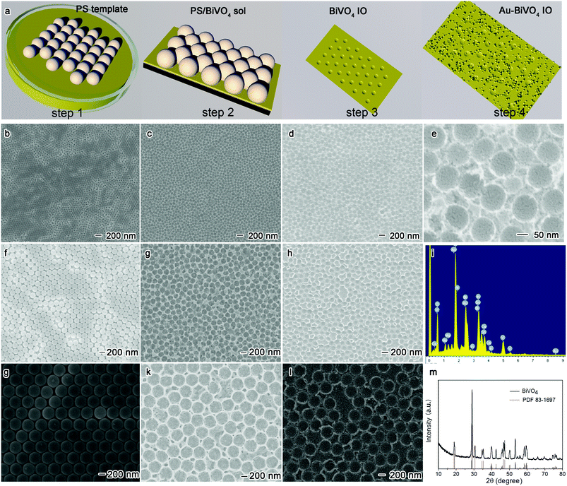
The Au–BiVO4 IO was first prepared through template-assisted self-assemble method, followed by electron-beam evaporation and the detailed procedures are illustrated in Fig. 1a. Briefly, PS spheres were self-assembled on the interface of BiVO4 sol and air to form the dense packed monolayer (step 1). With the capillary force, the BiVO4 sol adsorbed at the bottom of the dense packed monolayer and transferred to the ITO glass (step 2). Followed by annealing process, PS spheres were removed leaving the BiVO4 IO (step 3). By electron-beam evaporation methods, Au nanoparticles can be loaded onto the BiVO4 IO, forming the tight connect between them (step 4).Then, the morphologies and microstructures of as-constructed monolayer PS spheres (100 nm), BiVO4 IO and Au crystal decorated BiVO4 IO were identified through SEM, and the results are exhibited in Fig. 1b–e. As shown in Fig. 1b and c, the single layer PS spheres are dense packed in hexagonal structure and the BiVO4 nano bowl array inherited the hexagonal structure after removing PS spheres, showing the periodic array. In addition, after introduction of the electron-beam evaporation, the Au nanoparticles with the size of ca. 10 nm were found to be densely distributed on the BiVO4 nano bowl array (see Fig. 1d and e). According to previous studies, such densely packed Au nanoparticles can be beneficial to induce electromagnetic field for enhancing the visible light utilization of the photocatalytic system. To further confirm the distribution of the Au nanoparticles on the BiVO4, the EDS characterization was performed. As shown in Fig. 1i, the Au, Bi, V and O elements were homogenously distributed on the samples, confirming the uniform existence of these elements on the prepared samples. Furthermore, the SEM images of reference samples, including 200 nm and 500 nm monolayer PS spheres and the corresponding BiVO4 nano array, were shown in Fig. 1f–l, suggesting that they own similar structure to the Au–BiVO4 IO. Moreover, the XRD patterns in Fig. 1m confirms the monoclinic scheelite BiVO4, consistent with PDF card 83-1697.
It is well-known that the large porous structure can substantially contribute to the enlarged specific surface area and enhanced catalytic sites. In this regard, we evaluate the physical properties of our prepared BiVO4 IO with different porous sizes of 100, 200 and 500 nm through N2 adsorption–desorption isotherm, and the results are shown in Fig. 2a–c. Generally, the specific surface area of the 100 nm, 200 nm and 500 nm BiVO4 inverse opal (on ITO substrate) was 2.05 m2 g−1, 1.263 m2 g−1 and 0.736 m2 g−1, separately. By excluding the influence of the ITO glass substrate which owns a specific surface area of 12.6 cm2 g−1, the actual specific surface area for BiVO4 inverse opal (100 nm) can be calculated to be 1627 cm−2 cm−2 by specific surface area of BiVO4 inverse opal divided that for ITO glass. Accordingly, the specific surface area for BiVO4 inverse opal with the porous sizes of 200 nm and 500 nm can be confirmed to be 1000.3 cm−2 cm−2 and 584 cm−2 cm−2, respectively. Clearly, the BiVO4 IO demonstrates a very high specific surface area due to its porous structure, which can provide more active sites and effectively enhance the contact of the catalysts with reactants.
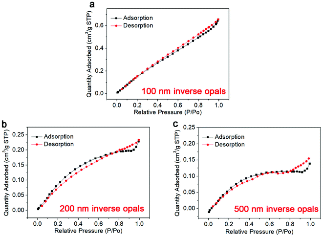 | ||
| Fig. 2 N2 adsorption–desorption isotherms of BiVO4 IO with period of (a) 100 nm, (b) 200 nm and (c) 500 nm. | ||
3.2 Photoelectrochemical measurements
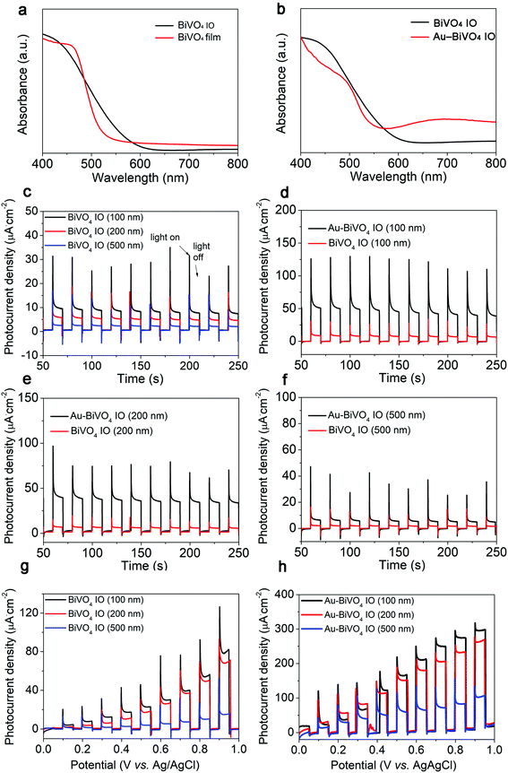
The photocatalytic water splitting performance of the prepared samples was determined through a PEC system. Prior to the test, the optical properties of the prepared samples were studied. As shown in Fig. 3a, compared with BiVO4 film, absorption band of BiVO4 IO exhibited a red shift, suggesting its improved light utilization capability, which was mainly attributed to the slow light effect caused by IO photonic bandgap.35,36 Notably, the pure BiVO4 IO owns noticeable absorption at 600 nm, enhancing the light scattering within its IO structure, which was beneficial for enhancing the light utilization of the photocatalytic system. After introduction of Au nanoparticles, two wide absorbance enhancement can be observed at ca. 500 and 650 nm, as shown in Fig. 3b. The absorption enhancement at this frequency band should be attributed to the intrinsic absorption of Au nanocrystal and plasmon resonance absorption of dense Au nanoparticles. Furthermore, there is an overlap in the second plasmonic peak of Au nanoparticles with the enhanced light absorption of the IO structure of BiVO4. Such an overlap can enhance the light utilization ability of the Au nanoparticles, and thus further boosting the function of SPR effect on the BiVO4.To reach the efficient photocatalyst for water splitting, its photocurrent density should be always optimized. In this sense, we determined the photocurrent density–time (I–t) curve for the different samples through a three-electrode electrochemical system at an applied bias voltage of 0.7 V vs. Ag/AgCl. Generally, the nanoarray structure can realize multiple reflection and scattering of incident light, thereby enhancing the light utilization capability of the photocatalyst toward improved photocurrent density. Therefore, as shown in Fig. 3c, the proper tuned BiVO4 IO (100 nm) exhibited the highest photocurrent density among all the prepared sample, because the moderate porous structure is beneficial for making full use of large specific surface area and unique light-scattering capability. More importantly, such a superior photocurrent density performance of the BiVO4 IO can be further improved by introduction of the Au nanoparticles. As shown in Fig. 3d, the photocurrent density of Au–BiVO4 IO (100 nm) was ca. 3 times enhanced in comparison with that of BiVO4 IO. This result is because the SPR effect of Au nanoparticles can induce a built-in electric field at its contact interface with the BiVO4, which can facilitate the photogenerated charge carrier migration, and thus further improve the photocurrent generation on the Au–BiVO4. Apart from that, as shown in Fig. 3d–f, the photocurrent density of Au–BiVO4 IO (100 nm) was also higher than that of Au–BiVO4 IO (200 nm) and Au–BiVO4 IO (500 nm), suggesting that the moderate porous structure can have the highest interaction with the plasmonic effect of Au. In addition, we perform the photocurrent–potential (I–V) curves for the above six samples and the results are shown in Fig. 3g and h. Generally, the photocurrent density gradually increases with the increase in applied bias potential, suggesting the high stability of the Au–BiVO4.
The average charge carrier lifetimes play a dominant role in determining the photocatalytic performance of a material. To further evaluate the influence of enlarged specific surface area and improved light absorption capability on photocatalytic performance of the Au–BiVO4 IO, we carried out the transient open-circuit voltage decay (OCVD) measurements (Fig. 4a) and calculated the corresponding average carrier lifetimes for the three composite samples (Fig. 4b). Similar to the above results, as shown in Fig. 4b, the Au–BiVO4 IO (100 nm) demonstrated the longest photogenerated charge carrier lifetime, further confirming that the unique porous structure of inverse opal and plasmonic effect of Au nanoparticles can synergistically enhance the photoconversion efficiency of the Au–BiVO4 IO (100 nm).
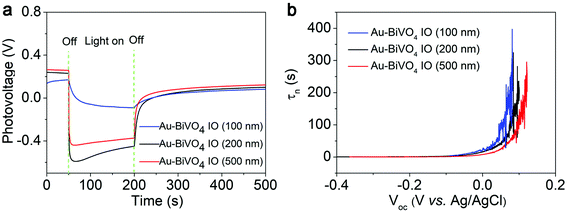 | ||
| Fig. 4 (a) OCVD curve and (b) average lifetimes of the photogenerated carriers (τn) obtained from the OCVD for Au nanocrystal decorated BiVO4 IO. | ||
3.3 Photocatalytic water oxidation
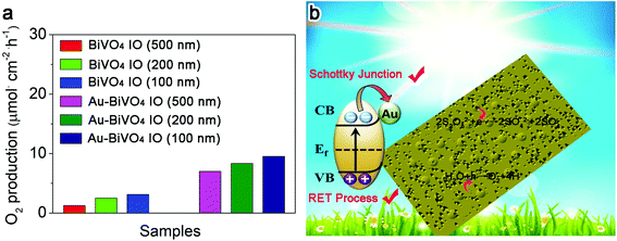
After studying the physicochemical and light-responsive properties of the prepared samples, we are in a position to utilize the prepared samples for photocatalytic water splitting. The resultant oxygen production performances of the various prepared samples are shown in Fig. 5a. As expected, the Au–BiVO4 IO (100 nm) exhibited the highest oxygen production rate among all the prepared samples. Such a superior performance of the Au–BiVO4 IO (100 nm) is mainly attributed the synergistic effect of the inverse opal structure and the plasmonic effect of Au. In detail, the inverse opal structure can endow the photocatalyst with large specific area and provide enormous surface active sites for the catalytic reaction. In addition, the plasmonic Au can induce an electric field around the BiVO4 and thus facilitate the photogenerated charge carrier separation efficiency. Most of all, the light-scattering effect of inverse opal structure can guarantee the optimized light utilization of Au, thereby intensifying the SPR effect of Au on enhancing the photocatalytic performance of BiVO4. As a result, the oxygen evolution rate of the Au–BiVO4 IO (100 nm) reached 9.56 μmol cm−2 h−1 through photocatalytic water splitting, which is about 3 times of the pure BiVO4 IO (100 nm).Based on the above results and discussion, the mechanism for the enhanced photocatalytic water splitting performance of the Au–BiVO4 can be illustrated and shown in Fig. 5b. Generally, the prepared BiVO4 IO owns a porous structure on its surface, which can endow it with large specific surface area and enormous surface active site. In addition, the loading of Au nanoparticles can introduce the SPR effect on the BiVO4 and induce an electric field at its interface with the BiVO4 for accelerating the photogenerated charge carrier migration. More importantly, the incorporation of inverse opal structure and plasmonic Au nanoparticles can stimulate a synergistic effect, where the multi-scattering of light within the inverse opal structure can guarantee the optimized light absorption of the Au nanoparticles. Therefore, the SPR effect of the Au nanoparticles can be boosted. For the detailed mechanism of the photocatalytic water splitting on Au–BiVO4, under light irradiation, the photogenerated electrons on the BiVO4 can migrate to the Au nanoparticles due to the formation of Schottky barrier attributed to the lower work function of Au. Then, the photogenerated electrons can further migrate to the surface of Au for S2O82− reduction, leaving the photogenerated holes on BiVO4 for water oxidation. The Schottky junction at the interface would prohibit the electron–holes recombination and promote charge transfer.
4 Conclusion
In summary, a series of BiVO4 IO and Au decorated BiVO4 IO were successfully constructed using the colloidal crystal template and electron beam evaporation methods. The SEM and BET results show the BiVO4 IO with high surface area, and Au nanocrystal was in tight contact with the BiVO4. The photoelectrochemical results indicated that Au–BiVO4 IO exhibited optimum photocatalytic activity under visible light irradiation, about 3 times higher than those of BiVO4. And the excellent water oxidation activity with oxygen of 9.56 μmol cm−2 h−1 was achieved. The superior photocatalytic activity of Au–BiVO4 IO can be mainly ascribed to synergetic effect of Schottky junction and RET process, leading to the effective separation the photo-generated electrons and holes for catalytic reaction. Consequently, this work would provide a useful technique for water oxidation under visible light irradiation.Conflicts of interest
There are no conflicts to declare.Acknowledgements
This work was supported by the Chinese Academy of Sciences President's International Fellowship Initiative (2019PC0114), China Postdoctoral Science Foundation (2019M652190) and Chinese Universities Scientific Fund (WK2060190096).References
- H. P. Lu, Z. Y. Huang, M. S. Martinez, J. C. Johnson, J. M. Luther and M. C. Beard, Energy Environ. Sci., 2020, 13, 1347 RSC
.
- T. Jia, J. B. Zhang, W. K. Zhong, Y. Y. Liang, K. Zhang, S. Dong, L. Ying, F. Liu, X. H. Wang, F. Huang and Y. Cao, Nano Energy, 2020, 72, 104718 CrossRef CAS
.
- K. Ren, S. Wang, Y. Luo, Y. Xu, M. Sun, J. Yu and W. Tang, RSC Adv., 2019, 9, 4816 RSC
.
- A.-A. Hoseini, S. Farhadi, A. Zabardasti and F. Siadatnasab, RSC Adv., 2019, 9, 24489 RSC
.
- J. Chen, X. P. Tao, C. Z. Li, Y. H. Ma, L. Tao, D. Y. Zheng, J. F. Zhu, H. Li, R. G. Li and Q. H. Yang, Appl. Catal., B, 2020, 262, 118271 CrossRef CAS
.
- Q. Wang and K. Domen, Chem. Rev., 2020, 120, 919 CrossRef CAS
.
- N. F. Ramli, P. N. A. Fahsyar, N. A. Ludin, M. A. M. Teridi, M. A. Ibrahim, S. H. Zaidi and S. Sepeai, Surf. Interfaces, 2019, 17, 100341 CrossRef CAS
.
- S. Zhang, T. Yu, H. Wen, R. Guo, J. Xu, R. Zhong, X. Li and J. You, RSC Adv., 2020, 10, 16892 RSC
.
- Y. W. Jo, C. Loka, K.-S. Lee and J.-H. Lim, RSC Adv., 2020, 10, 16187 RSC
.
- S. Chen, D. L. Huang, G. M. Zeng, W. J. Xue, L. Lei, P. Xu, R. Deng, J. Li and M. Cheng, Chem. Eng. J., 2020, 382, 122840 CrossRef CAS
.
- Q. Xie, W. M. He, S. W. Liu, C. H. Li, J. F. Zhang and P. K. Wong, Chin. J. Catal., 2020, 41, 140 CrossRef CAS
.
- M. Mehta, S. Krishnamurthy, S. Basu, T. P. Nixon and A. P. Singh, Mater. Today Chem., 2020, 17, 100283 CrossRef CAS
.
- V. Andrei, B. Reuillard and E. Reisner, Nat. Mater., 2020, 19, 189 CrossRef CAS
.
- P. Guan, H. Bai, F. Wang, H. Yu, D. Xu, W. Fan and W. Shi, Chem. Eng. J., 2019, 358, 658 CrossRef CAS
.
- J. H. Kim and J. S. Lee, Adv. Mater., 2019, 31, 1806938 CrossRef
.
- W. Zhao, Y. Feng, H. Huang, P. Zhou, J. Li, L. Zhang, B. Dai, J. Xu, F. Zhu, N. Sheng and D. Y. C. Leung, Appl. Catal., B, 2019, 245, 448 CrossRef CAS
.
- C. Liu, X. Zhang, W. Li, Y. Yu, M. Liu, L. Wang, C. Li, X. Zhang, X. Li and X. Lin, Mater. Res. Bull., 2020, 122, 110640 CrossRef CAS
.
- Z. Zhang, X. Jiang, J. Mei, Y. Li, W. Han, M. Xie, F. Wang and E. Xie, Chem.
Eng. J., 2018, 331, 48 CrossRef CAS
.
- T.-G. Vo, C.-C. Kao, J.-L. Kuo, C.-c. Chiu and C.-Y. Chiang, Appl. Catal., B, 2020, 278, 119303 CrossRef CAS
.
- Q. J. Shi, Z. J. Li, L. Chen, X. L. Zhang, W. H. Han, M. Z. Xie, J. L. Yang and L. Q. Jing, Appl. Catal., B, 2019, 244, 641 CrossRef CAS
.
- Y.-S. Chen and L.-Y. Lin, J. Power Sources, 2019, 436, 226842 CrossRef CAS
.
- T. G. U. Ghobadi, A. Ghobadi, M. C. Soydan, M. B. Vishlaghi, S. Kaya, F. Karadas and E. Ozbay, Chemsuschem, 2020, 13, 2577 CrossRef CAS
.
- V. Likodimos, Appl. Catal., B, 2018, 230, 269 CrossRef CAS
.
- J. Liu, J. Jin, Y. Li, H.-W. Huang, C. Wang, M. Wu, L.-H. Chen and B.-L. Su, J. Mater. Chem. A, 2014, 2, 5051 RSC
.
- A. Lavin, R. Sivasamy, E. Mosquera and M. J. Morel, Surf. Interfaces, 2019, 17, 100367 CrossRef CAS
.
- B. Li, R. Wang, X. Shao, L. Shao and B. Zhang, Inorg. Chem. Front., 2017, 4, 2088 RSC
.
- R. Wang, B. Li, Y. Xiao, X. Tao, X. Su and X. Dong, J. Catal., 2018, 364, 154 CrossRef CAS
.
- G. Qiu, R. Wang, F. Han, X. Tao, Y. Xiao and B. Li, Ind. Eng. Chem. Res., 2019, 58, 17389 CrossRef CAS
.
- B. Li, B. Zhang, S. Nie, L. Shao and L. Hu, J. Catal., 2017, 348, 256 CrossRef CAS
.
- J. Xue, S. Ma, Y. Zhou and Q. Wang, RSC Adv., 2015, 5, 88249 RSC
.
- J. Zeng, T. Song, M. Lv, T. Wang, J. Qin and H. Zeng, RSC Adv., 2016, 6, 54964 RSC
.
- R. E. Adam, M. Pirhashemi, S. Elhag, X. Liu, A. Habibi-Yangjeh, M. Willander and O. Nur, RSC Adv., 2019, 9, 8271 RSC
.
- X. Wang, R. Long, D. Liu, D. Yang, C. Wang and Y. Xiong, Nano Energy, 2016, 24, 87 CrossRef CAS
.
- W. Ye, R. Long, H. Huang and Y. J. Xiong, J. Mater. Chem. C, 2017, 5, 1008 RSC
.
- F. Sordello and C. Minero, Appl. Catal., B, 2015, 163, 452 CrossRef CAS
.
- B. Cakiroglu and M. Ozacar, Biosens. Bioelectron., 2019, 141, 111385 CrossRef CAS
.
| This journal is © The Royal Society of Chemistry 2021 |

