
 Open Access Article
 This Open Access Article is licensed under a Creative Commons Attribution-Non Commercial 3.0 Unported Licence
Boosting light harvesting and charge separation of WO3 via coupling with Cu2O/CuO towards highly efficient tandem photoanodes†
Mahmoud A. Khalifaab,
Luying Shena,
Jianming Zheng*a and
Chunye Xu *a
*a
aHefei National Laboratory for Physical Sciences at the Microscale, CAS Key Laboratory of Soft Matter Chemistry, Department of Polymer Science and Engineering, University of Science and Technology of China, Hefei 230026, P. R. China. E-mail: jmz@ustc.edu.cn; chunye@ustc.edu.cn
bPhysics Department, Faculty of Science, Mansoura University, Mansoura 35516, Egypt
First published on 12th April 2021
Abstract
Photoanodes based on semiconductor WO3 have been attractive due to its good electron mobility, long hole-diffusion length, and suitable valence band potential for water oxidation. However, the semiconductor displays disadvantages including a relatively wide bandgap, poor charge separation and transfer, and quick electron–hole recombination at the interface with the electrolyte. Here we present a significantly improved photoanode with a tandem structure of ITO/WO3/Cu2O/CuO, which is prepared first by hydrothermally growing a layer of WO3 on the ITO surface, then by electrodepositing an additional layer of Cu2O, and finally by heat-treating in the air to form an exterior layer of CuO. Photocurrent measurements reveal that the prepared photoanode produces a maximum current density of 4.7 mA cm−2, which is, in comparison, about 1.4 and 5.5 times the measured values for ITO/WO3/Cu2O and ITO/WO3 ones, respectively. These enhancements are attributed to (1) harvested UV, visible, and NIR light of the solar spectrum, (2) accelerated charge separation at the heterojunction between WO3 and Cu2O/CuO, (3) better electrocatalytic activity of formed CuxO than pure Cu2O, (4) formation of a protective layer of CuO. This study thus may lead to a promising way to make high-performance and low-cost photoanodes for solar energy harvesting.
1. Introduction
Photoelectrochemical (PEC) water splitting has been considered to be a promising pathway for solar energy conversion.1,2 In general, a PEC cell consists of a semiconductor photoanode, a Pt counter electrode, and an aqueous electrolyte between them. In principle, the photoanode absorbs photons to generate electron–hole pairs, which are then separated and transferred to opposite electrodes for participating in water molecular splitting.3 Since the first discovery of a PEC cell with TiO2 in 1972,4 various photoanode semiconductor materials, including transition metal oxides, Fe2O3, WO3, BiVO4, and ZnO, have been reported.5–8Among them, tungsten trioxide (WO3) is a promising photoanode semiconductor used for PEC cells, due to its unique properties such as good electron mobility (∼12 cm2 V−1 s−1), long hole diffusion length (∼150 nm), non-toxic, low cost, and appropriate valance band (VB) for water oxidation.9,10 However, it captures only approximately 12% of the solar spectrum and suffers from rapid electron–hole recombination and slow transfer for photogenerated charge carriers at the photoanode/electrolyte interface, which seriously limits its PEC performance.11 To overcome these drawbacks, studies with different approaches, such as doping with hetero-elements,12,13 decorating with co-catalysts,14,15 manipulating of nanostructured WO3,16,17 and coupling with another semiconductor to form heterojunction,18,19 have been carried out. Among these studies, photoanodes that couple WO3 with p-Cu2O are considered to be one of the most promising strategies to promote charge separation and widen absorption.9,20–22 For instance, Zhang J. et al. prepared WO3/Cu2O heterojunctions by electrodepositing different amounts of Cu2O on the surface of the WO3 film.20 They found the highest photocurrent density was significantly improved by about 3.51 times higher than that of pristine WO3, and this result is mainly attributed to the formation of p–n heterojunction and broaden solar absorption. We are aiming to extend these studies to achieve a more efficient photoanode by broadening the photoresponse range. The tandem cell is designed to achieve full use of the solar spectrum (UV, visible, and NIR regions).23 As CuO has a narrower bandgap of ∼1.4 eV than Cu2O of ∼2.1 eV,24 it is expected to absorb lights in the NIR region. Thus, the tandem structure of WO3/Cu2O/CuO can harvest the whole solar spectrum due to WO3, Cu2O, and CuO layers are responsive to UV, visible, and NIR regions, respectively. The ITO/WO3/Cu2O photoanodes with electrodepositing different amounts of Cu2O are investigated first in order to obtain an appropriate thickness of Cu2O with optimal catalytic activity and then form Cu2O/CuO by heat-treating.
In this work, a photoanode with the tandem structure of ITO/WO3/Cu2O/CuO is prepared and investigated. ITO/WO3/Cu2O/CuO structure is designed to enhance light harvesting and electron–hole pairs separation. It is systematically characterized in terms of structural, morphological, optical, and PEC properties. Its PEC performance is evaluated in comparison with these of photoanodes based on ITO/WO3/Cu2O and ITO/WO3. As expected, significantly improved PEC performance of the as-prepared photoanode was achieved with a photocurrent density of 4.7 mA cm−2 at 1.23 V versus reversible hydrogen electrode (RHE) under AM1.5G illumination, which is approximately 5.5 times that of pristine WO3. These results demonstrate that ITO/WO3/Cu2O/CuO may be regarded as a promising, simple, and low-cost photoanode for solar energy harvesting.
2. Experimental details
2.1. Chemicals
Sodium tungstate dehydrates (Na2WO4–2H2O), sodium chloride (NaCl), copper sulfate (CuSO4), lactic acid (C3H6O3), sodium hydroxide (NaOH), sodium sulfate (Na2SO4), and hydrochloric acid (HCl) were obtained from Sinopharm Chemical Reagent Co. Ltd. All the chemicals have been used directly without further purification.2.2. Fabrication of ITO/WO3 photoanodes
WO3 film was directly synthesized on an indium tin oxide (ITO) substrate by the hydrothermal method reported previously.25,26 As a cleaning procedure, ITO glass substrates were ultrasonicated consecutively in acetone, ethanol and DI water, and each process took 30 min. The solution was prepared, under vigorous stirring, first by dissolving 0.83 g Na2WO4–2H2O in 19 mL DI water in a 50 mL beaker, then by adding 3 M HCl to reach pH 2.2, further by adding 0.29 g NaCl. The reaction took place in a Teflon-lined hydrothermal synthesis autoclave reactor at 180 °C for 150 min, where the cleaned ITO glass substrates (2.5 × 5 cm) were immersed with their conductive faces down in the precursor solution. After the reaction, uniform WO3 films were obtained on the ITO substrates; they were rinsed extensively with deionized water and dried on a muffle furnace at 300 °C for a half-hour for usage.2.3. Fabrication of ITO/WO3/Cu2O photoanodes
As intermediate samples, ITO/WO3/Cu2O photoanodes were made by electrodepositing a Cu2O layer onto the prepared WO3 surface. The bath solution for the process is an aqueous solution of 0.4 M copper sulfate and 3.0 M lactic acid, with an adjusted pH 12.0 by adding a controlled amount of 4.0 M NaOH. The electrochemical deposition was carried out with the three-electrode system where the prepared ITO/WO3 substrate was used as the working electrode, a platinum plate as the counter electrode, and an Ag/AgCl wire as the reference electrode. The conditions set for the deposition include bath temperature at 60 °C, deposition potential of −0.4 V, and varied deposition times of 1, 5, 10, 15 min. Under such conditions, uniform Cu2O films on the WO3 substrates were obtained for all the samples in this experiment.2.4. Fabrication of ITO/WO3/Cu2O/CuO photoanodes
WO3/Cu2O/CuO photoanodes were obtained by annealing the prepared WO3/Cu2O photoanodes in a muffle furnace at a suitable temperature (∼300 °C) for a suitable time (∼1 h) to oxidize their Cu2O surfaces into CuO ones. The whole process for fabricating the WO3/Cu2O/CuO photoanodes is shown as a schematic in Fig. 1.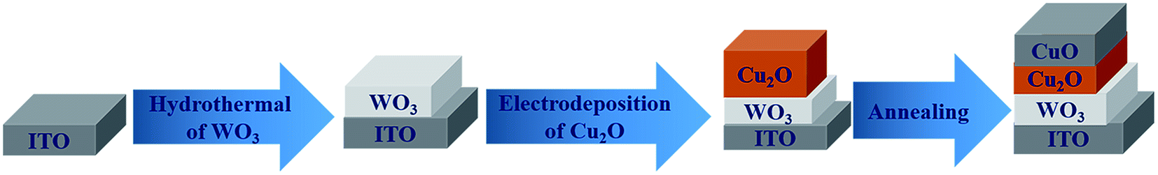 | ||
| Fig. 1 Schematic diagram for fabricating ITO/WO3/Cu2O/CuO photoanodes. | ||
2.5. Characterization
The prepared photoanodes were characterized for the crystal structures by using X-ray diffraction (X'Pert PRO; PANalytical B.V., Almelo, Netherlands), where Cu Kα (Kα = 1.5406 Å, 40 kV, 200 mA) was used as the X-ray source. Their elemental compositions were investigated by using X-ray photoelectron spectroscopy (XPS, ESCALAB 250, Thermo-VG Scientific, East Grinstead, West Sussex, UK), with an Al Kα as the X-ray source. Their surface morphologies were measured with a scanning electron microscopy (SEM, Sirion 200, FEI, Hillsboro, Oregon, USA), equipped with an X-ray energy dispersive spectrometer, and a Field Emission Transmission Electron Microscope (FETEM, JEOL JEM-2100F). Their optical absorbance was measured by using a UV-vis-NIR spectrophotometer (V-670, Jasco, Tokyo, Japan). Their photoelectrochemical and photocurrent density measurements were evaluated in a three-electrode system by using the as-prepared photoanodes as the working electrode, Pt as a counter electrode and Ag/AgCl as a reference electrode in 0.5 M Na2SO4 (pH 7.0) electrolyte under simulated AM1.5 illumination. A 300 W Xe lamp (Perfect Light Company) was used as an illumination source.The light source intensity was calibrated with an FZ-A irradiator-meter (Photoelectric Instrument Factory, China) to simulate AM1.5 illuminations (100 mW cm−2). The measured potential versus Ag/AgCl (EAg/AgCl) was transformed to that versus reversible hydrogen electrode (RHE) using Nernst equation:27
| ERHE = EAg/AgCl + 0.0591 × pH + 0.1976 V |
Electrochemical impedance spectroscopy (EIS) measurements were carried out at 20 mV s−1 scan speed and frequency ranging from 0.1 Hz to 105 Hz.
3. Results and discussion
The crystal structure of the fabricated ITO/WO3/Cu2O/CuO tandem photoanodes is revealed with X-ray diffraction (XRD) analysis, in comparison with these of the precursor photoanodes. The results are shown in Fig. 2. Apparently, WO3 (♣) is identical in diffraction peaks among three different types of photoanodes, which is indexed as a hexagonal WO3 (JCPDS no. 85-2460).25 As well, the amorphous WO3 is demonstrated by a broad hump between 2θ around 20° to 40°. Similarly, Cu2O (◆) shows the same peaks between ITO/WO3/Cu2O and ITO/WO3/Cu2O/CuO photoanodes, it is indexed as cubic phase (space group: Pn![[3 with combining macron]](https://www.rsc.org/images/entities/char_0033_0304.gif) m (224); JCPDS no. 65-3288), due to the diffraction peaks located at 2θ of 29.6°, 36.5°, 42.4°, 61.5° and 73.7°, which reflects (110), (111), (200), (220), and (311), respectively. Additionally, CuO (●) is indexed as a monoclinic crystal as well (space group: C2/c (15); JCPDS no. 65-2309). These results demonstrate that the tandem photoanodes are constituted of layered crystals of WO3, Cu2O, and CuO.
m (224); JCPDS no. 65-3288), due to the diffraction peaks located at 2θ of 29.6°, 36.5°, 42.4°, 61.5° and 73.7°, which reflects (110), (111), (200), (220), and (311), respectively. Additionally, CuO (●) is indexed as a monoclinic crystal as well (space group: C2/c (15); JCPDS no. 65-2309). These results demonstrate that the tandem photoanodes are constituted of layered crystals of WO3, Cu2O, and CuO.
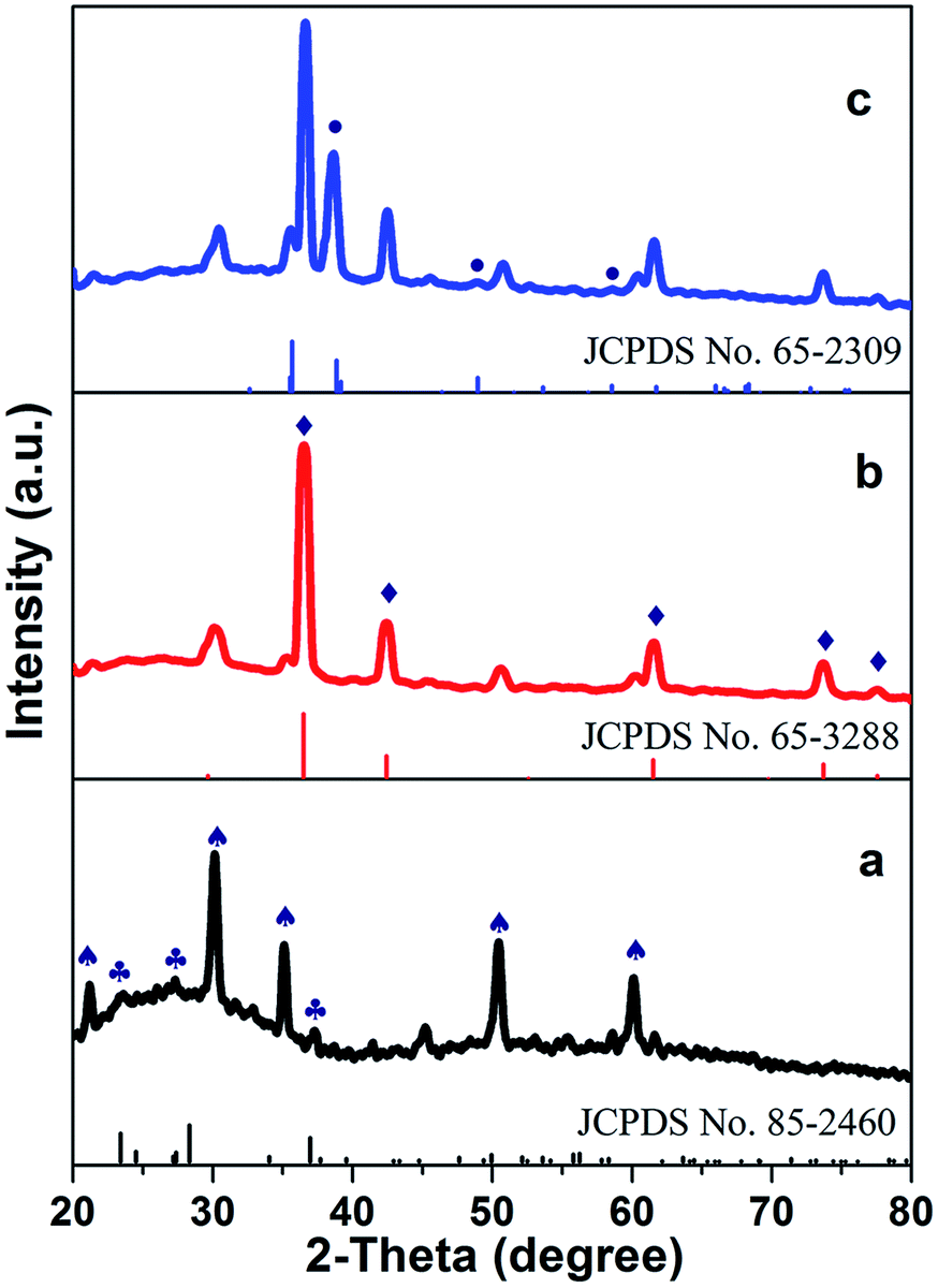 | ||
| Fig. 2 XRD patterns of (a) ITO/WO3, (b) ITO/WO3/Cu2O and (c) ITO/WO3/Cu2O/CuO photoanodes. The mark ♠ is denoted for ITO, ♣ for WO3, ◆ for Cu2O, and ● for CuO. | ||
To gain more insight into the chemical composition of photoanodes, XPS measurements were carried out for all three types of the obtained photoanodes. For the basic ITO/WO3 photoanode, three well-resolved peaks at the binding energy of 35.5, 37.8 and 41.2 eV are observed (Fig. 3a), which are attributed to the spin–orbit split peaks of W 4f7/2, W 4f5/2 and W 4f3/2, respectively.25 On the other hand, its O 1s core-level XPS spectrum (Fig. 3b) contains one asymmetric peak, from which two fitted peaks centered at the binding energy of 530.6 and 532.5 eV can be obtained. The former corresponds to W–O bonds from the crystals, whereas the latter is related to W–OH bonds near the surface.9 These results indicate that this photoanode is fully covered with WO3 crystals. Similarly, a full formation of the crystal Cu2O layer on the basic ITO/WO3 photoanode is also confirmed. Fig. 3c and d present the XPS spectra for Cu and O bonds of the prepared ITO/WO3/Cu2O photoanode, respectively. Obviously, only two peaks centered at 932.6 and 952.3 eV are observed, which corresponds to Cu 2p3/2 and Cu 2p1/2 of Cu2O, respectively.24 The fitted two peaks centered at 530.5 and 532.5 eV (Fig. 3d) correspond to the oxygen ions of the oxide and its surface group of OH− and residual water that is left during wet processing. By heating the ITO/WO3/Cu2O photoanode in the open air, its surface Cu2O is expected to be oxidized into CuO. As expected, other than the peaks for Cu2O, two additional fitted peaks centered at 933.6 and 953.4 eV appear (Fig. 3e). The new peaks are assigned to the formation of CuO.24 However, only one peak for oxygen ions is found for the heat-treated photoanode (Fig. 3f). This is attributed to the removal of residual water and prevention from surface hydroxylation of the subjected photoanode under temperature treatment.
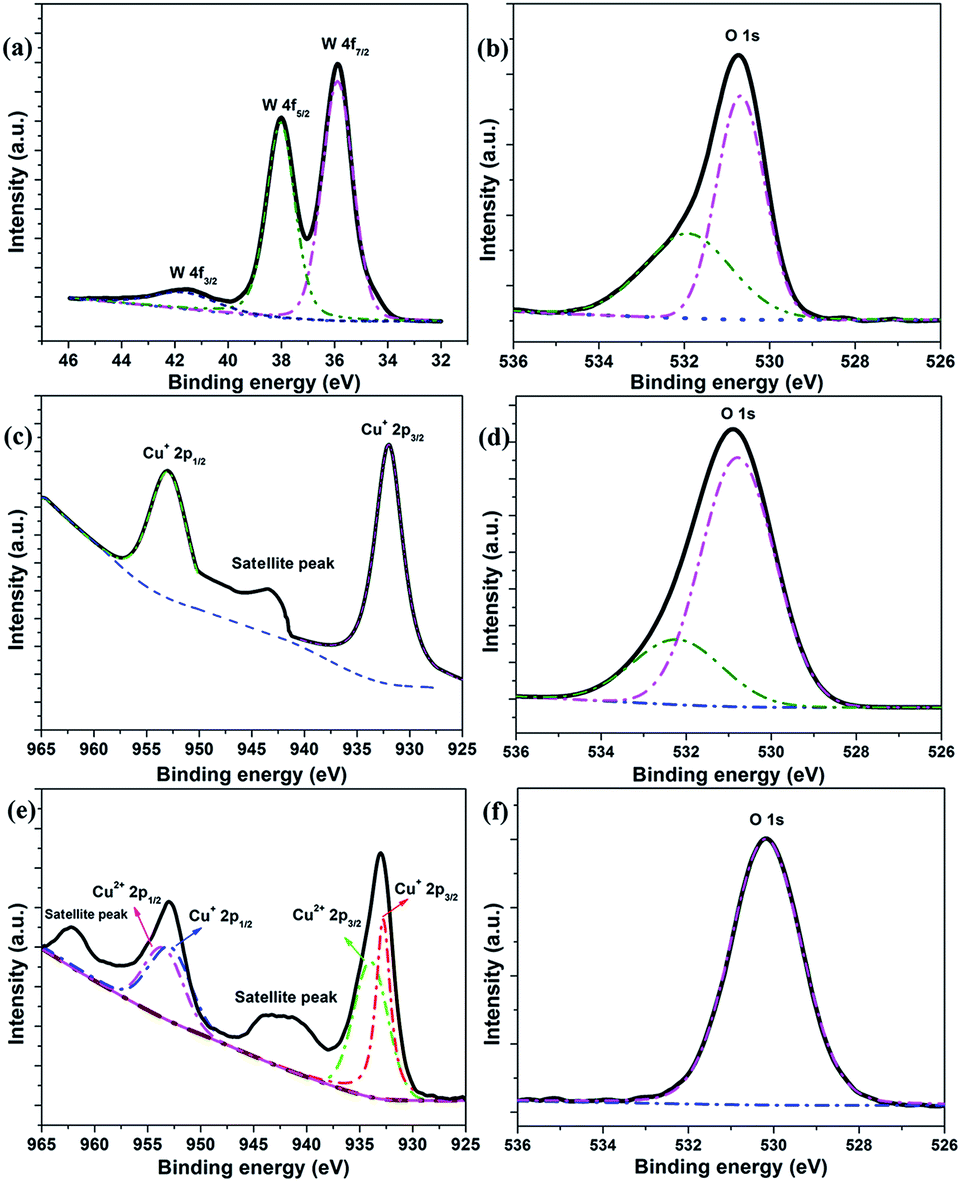 | ||
| Fig. 3 XPS spectra of the prepared photoanodes. (a) W 4f and (b) O 1s for ITO/WO3, (c) Cu 2p and (d) O 1s for ITO/WO3/Cu2O, and (e) Cu 2p and (f) O 1s for ITO/WO3/Cu2O/CuO photoanode. | ||
The surface morphology of the synthesized photoanodes is investigated. For the basic photoanode ITO/WO3, its surface morphology was discussed in our previous report.25,26 For the heterojunction photoanode of ITO/WO3/Cu2O, its surface morphology evolving with the formation of Cu2O is studied. Fig. 4a–d shows the surface SEM image of the photoanode prepared with an electrodeposition time for 1, 5, 10 and 15 min, respectively. Obviously, cubic grains of Cu2O are observed to form from the beginning and keep growing in density and size. At the deposition time of 15 min, the surface of the photoanode is fully covered with Cu2O grains. The prepared photoanode at 15 min was oxidized when it tested for PEC measurements, then the photoanode at 10 min has been selected to form a tandem photoanode. The surface morphology of ITO/WO3/Cu2O photoanode before and after annealing was measured and results are shown in Fig. 5. It can be seen that surface morphology is slightly changed after the annealing. The morphology is a compacted and truncated pyramid before annealing. After annealed, irregular small particles are grown on the pyramid surface and the optical color was changed from reddish-brown to black due to CuO formation. The outline of the pyramid shape still could be seen, which is agreed with the mentioned XRD that the annealed photoanode has a mixture of Cu2O and CuO. The cross-section SEM images of the ITO/WO3/Cu2O photoanode before and after annealing, with the highlight of WO3, Cu2O, CuO and ITO layers, are displayed in Fig. S1.† The annealed electrode slightly thicker than the as-prepared ITO/WO3/Cu2O due to the CuO particle formed on the top surface of the Cu2O.
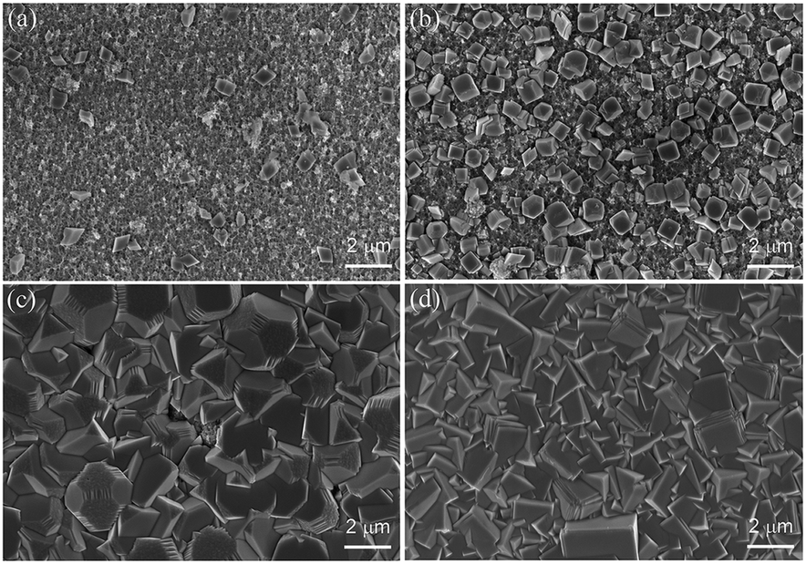 | ||
| Fig. 4 SEM images of ITO/WO3/Cu2O photoanodes prepared at different electrodeposition times for Cu2O layer formation: (a) 1 min, (b) 5 min, (c) 10 min and (d) 15 min. The scale bar is 2 μm. | ||
 | ||
| Fig. 5 SEM images of ITO/WO3/Cu2O photoanode (a) before and (b) after annealing at 300 °C in the open air. The scale bar is 2 μm. | ||
HRTEM analysis of the prepared photoanodes was measured to verify lattice fringes of the formed materials and the results are shown in Fig. 6. The regular spacing of 0.383 nm is observed in Fig. 6a, which is corresponded to the (002) plane of hexagonal WO3. Moreover, a d-spacing of 0.246 nm is shown in Fig. 6b and c, which is correlated to the (111) plane of Cu2O. Furthermore, the lattice spacing of 0.232 nm is assigned to the (111) plane of CuO. These results reveal that the lattice fringes of WO3, Cu2O and CuO are confirmed. HRTEM analysis has good agreement with XRD and XPS.
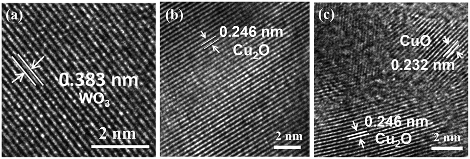 | ||
| Fig. 6 HRTEM images of the prepared photoanodes. Lattice fringes of (a) WO3 for ITO/WO3, (b) Cu2O for ITO/WO3/Cu2O, and (c) Cu2O and CuO for ITO/WO3/Cu2O/CuO photoanode. | ||
The optical absorbance spectra of the prepared photoanodes were measured by the UV-vis-NIR spectrophotometer and the results are shown in Fig. 7. Fig. 7a shows spectra of ITO/WO3/Cu2O photoanodes with varying electrodeposition times for the formation of the Cu2O layer. The absorption edge wavelength is shifted to a higher wavelength (is redshifted) with increasing the deposition time, which is moved from around 320 nm to ∼520 nm for 1 min and 15 min, respectively that can highly increase the visible light absorption from the solar spectrum. As shown in Fig. 7b, the absorption edge wavelength is moved from about 500 nm to around 645 nm for ITO/WO3/Cu2O and ITO/WO3/Cu2O/CuO, respectively which can increase solar energy harvesting. These enhancements are attributed to the optical absorbance and bandgap (Eg) of functional layers with the tandem design. Optical absorbance and the corresponding calculated bandgap (Eg) from the Tauc plot of each bare layer have been implemented28 and are presented in Fig. S2.† The absorption edges of WO3, Cu2O and CuO film are located at approximately 310 nm, 520 nm and 805 nm, which correlate to a bandgap of about 2.9 eV, 2.1 eV and 1.38 eV that responsive to UV light, visible light and NIR light, respectively.
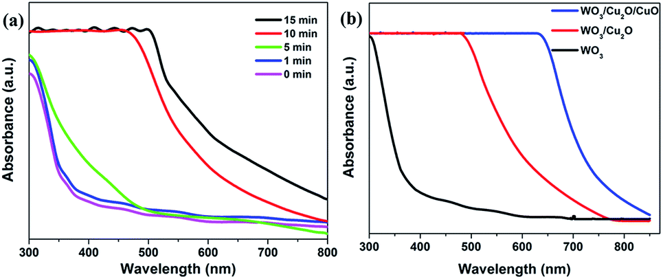 | ||
| Fig. 7 UV-vis absorption spectra of (a) ITO/WO3/Cu2O photoanodes prepared at different electrodeposition times for the formation of Cu2O layers and (b) photoanodes with varied functional layers. | ||
The linear sweep voltammetry (LSV) measurements were recorded to test the PEC performance and the results are displayed in Fig. 8. Fig. 8a shows the LSV curves of the ITO/WO3/Cu2O photoanodes with different electrodeposition times of the Cu2O layer. Clearly, photoanodes exhibit significantly increased photocurrent at 1.23 V vs. RHE with increasing electrodeposition time compared with pure ITO/WO3 photoanode. The highest achieved photocurrent density at 1.23 V vs. RHE is 3.4 mA cm−2, which was recorded at deposition time of 10 min and 15 min, compared with 0.85 mA cm−2 for ITO/WO3 photoanode. This significant improvement could mainly be attributed to the high absorption coefficient of Cu2O and the construction of a p–n heterojunction between Cu2O and WO3. Unfortunately, an excess of Cu2O amount may produce lattice scattering and decrease of charge carrier concentration20,21 that was happened for the photoanode at 15 min. An obvious peak is observed at 1.1 V vs. RHE and might be attributed to the oxidation of Cu2O. For the investigation, SEM images of the photoanode were measured before and after the PEC test and the result is shown in Fig. S3.† A small particle is formed on a pyramid shape, which is attributed to the oxidation of a small amount of Cu2O to Cu. Therefore, ITO/WO3/Cu2O at 10 min has been selected to fabricate a tandem photoanode. The ITO/WO3/Cu2O/CuO photoanode was formed by annealing of ITO/WO3/Cu2O in the open air. Fig. 8b presents the LSV plots of the functional photoanodes under light illumination (1 sun). As expected, ITO/WO3/Cu2O/CuO photoanode yields the highest photocurrent density of ∼4.7 mA cm−2 at 1.23 V vs. RHE, which is approximately about 1.4 and 5.5 times of the measured values for ITO/WO3/Cu2O and ITO/WO3 ones, respectively. These significant enhancements are attributed to the CuO layer that can extend light absorption and then increase the generation of electron–hole pairs29 with the charge-separation improvement as well.
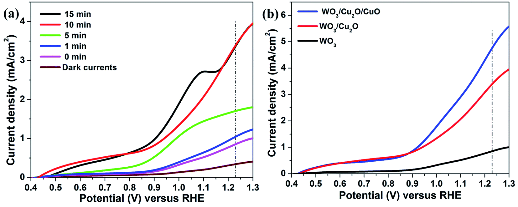 | ||
| Fig. 8 Linear sweep voltammetry curves of (a) ITO/WO3/Cu2O photoanodes prepared at different electrodeposition times for the formation of Cu2O layers and (b) photoanodes with varied functional layers. | ||
The charge carriers separation improvement could be ascribed to the p–n junction effect, which could induce the directional transfer of photogenerated holes and electrons to the copper oxide and WO3, respectively as shown in Fig. 9. The p–n junction influence can separate efficiently the generated electron–hole pairs. The photogenerated electron can transfer from the Cu2O conduction band to that of WO3, it would reduce hydrogen ion (H+) into hydrogen gas (H2). On the other hand, the photogenerated hole can move from the valence band of WO3 to that of Cu2O, it would oxidize water into oxygen gas (O2) and hydrogen ion (H+).9,21 The substantial enhancement in charge separation on ITO/WO3/CuxO photoanode indicates that CuxO coupling has a more obvious impact on the water oxidation kinetics of WO3 than that on the surface-charge carriers' separation of ITO/WO3 photoanode.30
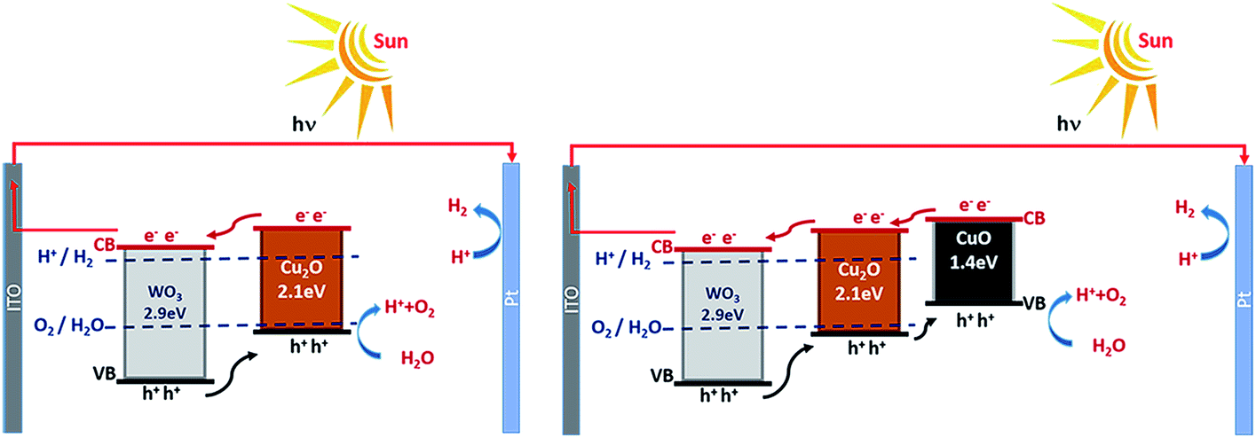 | ||
| Fig. 9 Schematic diagram of the charge carrier transfer mechanism on ITO/WO3/Cu2O and ITO/WO3/Cu2O/CuO photoanodes under simulated sunlight illumination. | ||
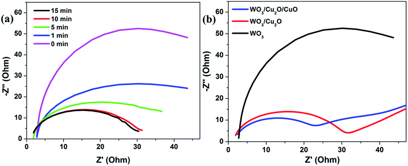
Electrochemical impedance spectroscopy (EIS) measurements were used to analyze the interfacial charge transfer properties of the prepared photoanodes. The experiments were carried out in a standard three-electrode system in a 0.5 M Na2SO4 aqueous solution with a 20 mV s−1 scan speed at AC potential of 20 mV vs. Ag/AgCl with a frequency ranging from 0.1 Hz to 105 Hz at room temperature under illumination. Fig. 10a shows Nyquist plots of ITO/WO3/Cu2O photoanodes at different electrodeposition times for the Cu2O layer. The diameter of the semicircle is indicative of the charge transfer resistance, Rct, between the photoanode and the electrolyte. It can be realized that the semicircle diameter is decreased with increasing electrodeposition time, which clearly indicates enhanced charge transfer and decreased the recombination rate of charge carriers at the interface between the photoanode and electrolyte, which agrees with previous results.20 As shown in Fig. 10b, the ITO/WO3/Cu2O/CuO photoanode has the smallest semicircle diameter compared with ITO/WO3/Cu2O and ITO/WO3 photoanode, which directs that the transfer of charge carrier from the photoanode to the electrolyte is increased due to the CuO layer formation and better electrocatalytic activity for water oxidation of CuxO compared with other photoanode.30 EIS results have a great agreement with the absorbance of prepared photoanodes and their PEC performance. Overall, these results illustrate that enhanced electrocatalytic activity can facilitate better transport of charge carriers that is an important contributor to the superior PEC performance.
 | ||
| Fig. 10 Nyquist plots of (a) ITO/WO3/Cu2O photoanodes prepared at different electrodeposition times for the formation of Cu2O layers and (b) photoanodes with varied functional layers. | ||
The photocurrent stability of the prepared photoanodes was evaluated with photocurrent time (J–t) measurements under illumination and the results are displayed in Fig. 11. As shown in Fig. 11a and b, the photocurrent of the photoanodes rises greatly under chopped light illumination and drops largely to zero when the light is off, indicating their excellent transient photoresponse. The photocurrent shows intense spikes instantaneously with turning on the light. These photocurrent spikes are followed by slow decaying until the light turns off. The existence of a spike-shaped photocurrent is related to the accumulation of charge carriers at the interface of the photoanode with electrolyte. The photoanodes show a quick response once the light turned on, good stability, and recyclability for all cycles under chopped light. As shown in Fig. 11, the ITO/WO3/Cu2O/CuO photoanode shows a higher photocurrent density and more good stability than ITO/WO3/Cu2O and ITO/WO3 photoanode, which is attributed to high generation of electron–hole pairs and fast charge carrier transfer. The stability enhancement of the photoanode may be correlated to the CuO layer served as a protected layer for the Cu2O31 and better catalytic ability of Cu2O/CuO with coupling with WO3. Moreover, it can be realized that with the forming of the CuO layer on the top surface of the ITO/WO3/Cu2O, more accumulation of charges occurs at the interface of the photoanode and electrolyte. When the light was turned on, the rate of charge carrier generation inside the ITO/WO3/Cu2O/CuO is more than that for the ITO/WO3/Cu2O. Also, the photocurrent decay during sun illumination is lower for the tandem photoanode, which suggests that decreasing charge carriers' recombination rate.
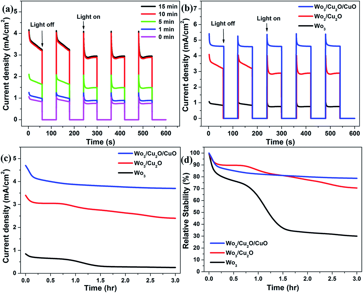 | ||
| Fig. 11 Evaluated stability of the prepared photoanodes. (a and b) Transient photocurrent of photoanodes was performed with a standard three-electrode system in a quartz glass beaker contained a 0.5 M Na2SO4 aqueous solution under chopped 1 sun illumination with period 60 s, on/off. (c) J–t and (d) relative stability curves of the photoanodes under continuous illumination for 3 hours. | ||
For a long time stability investigation, the J–t curves of the functional photoanodes have been recorded under continuous illumination for 3 hours as shown in Fig. 11c. The relative photocurrent stability is defined as the percent of photocurrent density at any time divided by the initial photocurrent. The relative stability of the ITO/WO3, ITO/WO3/Cu2O and ITO/WO3/Cu2O/CuO is 30%, 71% and 79%, respectively after illumination for 3 hours as presented in Fig. 11d. Photocurrent and stability of the ITO/WO3 photoanode are both constrained by its low absorption, poor surface separation and slow transfer for photogenerated charge carriers. The ITO/WO3/Cu2O photoanode has a photocurrent higher than ITO/WO3. But the chemical instability is an inherent drawback of Cu2O in aqueous solutions because the redox potentials for the reduction and oxidation of monovalent copper oxide lie within the bandgap.9 Therefore, it is still not too stable. Higher photocurrent and better stability are observed for the ITO/WO3/Cu2O/CuO photoanode in comparison with other photoanodes. These improvements are attributed to (1) harvested UV, visible, and NIR light of the solar spectrum, (2) accelerated charge separation at the heterojunction between WO3 and CuxO, (3) better electrocatalytic activity of formed CuxO, and (4) forming a protected layer of CuO.
4. Conclusions
The ITO/WO3/Cu2O/CuO tandem photoanode has been successfully fabricated for solar energy harvesting. WO3 layer was deposited on an ITO glass by hydrothermal method and then electrodeposited Cu2O on it, and finally oxidizing the Cu2O layer into a partial CuO layer. The structural, morphological, optical and PEC properties of photoanode were systematically investigated. PEC performance is boosted to achieve a photocurrent of 4.7 mA cm−2, which is about 1.4 times and 5.5 times higher than that for ITO/WO3/Cu2O and ITO/WO3 ones, respectively. The improvement could be attributed to (1) harvested the whole solar spectrum due to WO3, Cu2O and CuO layers are responsive to UV, visible and NIR regions, respectively, (2) accelerated charge separation at the heterojunction between WO3 and Cu2O/CuO, (3) better electrocatalytic activity of formed CuxO than pure Cu2O, (4) formation of a protective layer of CuO. Our results demonstrate that ITO/WO3/Cu2O/CuO could be a promising, low-cost and highly efficient photoanode for solar energy harvesting devices.Conflicts of interest
There are no conflicts to declare.Acknowledgements
Authors gratefully acknowledge financial support from the National Natural Science Foundation of China (Grant No. 21774114), the National Key R&D Program of China (Grant No. 2017YFA0403403), and CAS-TWAS President's Fellowship (awarded to Mahmoud A. Khalifa).References
- Y. Chen, X. Feng, M. Liu, J. Su and S. Shen, Nanophotonics, 2016, 5, 524 Search PubMed.
- Y. Rong, Y. Ma, F. Guo, J. Qian, H. Li, M. Zhou, Z. Xu, Y.-Q. Zheng and T.-T. Li, Int. J. Hydrogen Energy, 2019, 44, 28833–28840 CrossRef CAS.
- G. Zheng, J. Wang, H. Liu, V. Murugadoss, G. Zu, H. Che, C. Lai, H. Li, T. Ding, Q. Gao and Z. Guo, Nanoscale, 2019, 11, 18968–18994 RSC.
- A. Fujishima and K. Honda, Nature, 1972, 238, 37–38 CrossRef CAS PubMed.
- Y. Mei, T.-T. Li, J. Qian, H. Li and Y.-Q. Zheng, J. Mater. Sci., 2020, 55, 12864–12875 CrossRef CAS.
- Y. Liu, B. R. Wygant, K. Kawashima, O. Mabayoje, T. E. Hong, S.-G. Lee, J. Lin, J.-H. Kim, K. Yubuta, W. Li, J. Li and C. B. Mullins, Appl. Catal., B, 2019, 245, 227–239 CrossRef CAS.
- Z. Kang, H. Si, S. Zhang, J. Wu, Y. Sun, Q. Liao, Z. Zhang and Y. Zhang, Adv. Funct. Mater., 2019, 29, 1808032 CrossRef.
- M. Iqbal, Y. Wang, H. Hu, M. He, A. Hassan Shah, L. Lin, P. Li, K. Shao, A. Reda Woldu and T. He, Appl. Surf. Sci., 2018, 443, 209–216 CrossRef CAS.
- J. Y. Zheng, C. W. Kim, A. U. Pawar and Y. S. Kang, New J. Chem., 2017, 41, 755–762 RSC.
- Y. Li, Z. Liu, Z. Guo, M. Ruan, X. Li and Y. Liu, ACS Sustainable Chem. Eng., 2019, 7(14), 12582–12590 CAS.
- H. Gong, Y. Zhang, Y. Cao, M. Luo, Z. Feng, W. Yang, K. Liu, H. Cao and H. Yan, Appl. Catal., B, 2018, 237, 309–317 CrossRef CAS.
- Y. Liu, J. Li, W. Li, Y. Yang, Y. Li and Q. Chen, J. Phys. Chem. C, 2015, 119, 14834–14842 CrossRef CAS.
- X. Yin, W. Qiu, W. Li, K. Wang, X. Yang, L. Du, Y. Liu and J. Li, Int. J. Hydrogen Energy, 2020, 45, 19257–19266 CrossRef CAS.
- R. Liu, Y. Lin, L. Y. Chou, S. W. Sheehan, W. He, F. Zhang, H. J. M. Hou and D. Wang, Angew. Chem., Int. Ed., 2011, 50, 499–502 CrossRef CAS PubMed.
- J. A. Seabold and K. S. Choi, Chem. Mater., 2011, 23, 1105–1112 CrossRef CAS.
- X. Feng, Y. Chen, Z. Qin, M. Wang and L. Guo, ACS Appl. Mater. Interfaces, 2016, 8, 18089–18096 CrossRef CAS PubMed.
- S. Wang, H. Chen, G. Gao, T. Butburee, M. Lyu, S. Thaweesak, J.-H. Yun, A. Du, G. Liu and L. Wang, Nano Energy, 2016, 24, 94–102 CrossRef CAS.
- M. Yang, H. He, H. Zhang, X. Zhong, F. Dong, G. Ke, Y. Chen, J. Du and Y. Zhou, Electrochim. Acta, 2018, 283, 871–881 CrossRef CAS.
- C. Liu, Y. Yang, J. Li, S. Chen, W. Li and X. Tang, Chem. Eng. J., 2017, 326, 603–611 CrossRef CAS.
- J. Zhang, H. Ma and Z. Liu, Appl. Catal., B, 2017, 201, 84–91 CrossRef CAS.
- L. J. Minggu, K. H. Ng, H. A. Kadir and M. B. Kassim, Ceram. Int., 2014, 40, 16015–16021 CrossRef CAS.
- G. Zheng, J. Wang, H. Li, Y. Li and P. Hu, Appl. Catal., B, 2020, 265, 118561 CrossRef.
- M. S. Prévot and K. Sivula, J. Phys. Chem. C, 2013, 117, 17879–17893 CrossRef.
- A. A. Dubale, C.-J. Pan, A. G. Tamirat, H.-M. Chen, W.-N. Su, C.-H. Chen, J. Rick, D. W. Ayele, B. A. Aragaw, J.-F. Lee, Y.-W. Yang and B.-J. Hwang, J. Mater. Chem. A, 2015, 3, 12482–12499 RSC.
- G. Luo, L. Shen, J. Zheng and C. Xu, J. Mater. Chem. C, 2017, 5, 3488–3494 RSC.
- L. Shen, G. Luo, J. Zheng and C. Xu, Electrochim. Acta, 2018, 278, 263–270 CrossRef CAS.
- G. Zheng, J. Wang, H. Li, Y. Li and P. Hu, Appl. Catal., B, 2019, 118561 Search PubMed.
- Y. Li, Z. Liu, M. Ruan, Z. Guo and X. Li, ChemSusChem, 2019, 12, 5282–5290 CrossRef CAS.
- S. K. Baek, J. S. Kim, Y. D. Yun, Y. B. Kim and H. K. Cho, ACS Sustainable Chem. Eng., 2018, 6, 10364–10373 CrossRef CAS.
- Y. Yang, X. Zhong, K. Liu, J. Du, Y. Yang, H. He, Y. Zhou, F. Dong, C. Fu and J. Wang, J. Electrochem. Soc., 2019, 166, H513–H520 CrossRef CAS.
- Y. Yang, D. Xu, Q. Wu and P. Diao, Sci. Rep., 2016, 6, 35158 CrossRef CAS.
Footnote |
| † Electronic supplementary information (ESI) available. See DOI: 10.1039/d1ra00417d |
| This journal is © The Royal Society of Chemistry 2021 |