
 Open Access Article
 This Open Access Article is licensed under a
 Creative Commons Attribution 3.0 Unported Licence
Two-dimensional blue phosphorene–BAs vdW heterostructure with optical and photocatalytic properties: a first-principles study
Khang D. Phamab,
C. V. Nguyen c,
Nguyen T. T. Binhd,
Cuong Q. Nguyen*ef,
M. Idreesg,
B. Aminh,
Son-Tung Nguyeni and
Nguyen V. Hieu*j
c,
Nguyen T. T. Binhd,
Cuong Q. Nguyen*ef,
M. Idreesg,
B. Aminh,
Son-Tung Nguyeni and
Nguyen V. Hieu*j
aLaboratory of Applied Physics, Advanced Institute of Materials Science, Ton Duc Thang University, Ho Chi Minh City, Vietnam. E-mail: phamdinhkhang@tdtu.edu.vn
bFaculty of Applied Sciences, Ton Duc Thang University, Ho Chi Minh City, Vietnam
cDepartment of Materials Science and Engineering, Le Quy Don Technical University, Ha Noi, Vietnam
dDepartment of Physics, Quang Binh University, Quang Binh, Vietnam
eInstitute of Research and Development, Duy Tan University, Da Nang 550000, Vietnam. E-mail: nguyenquangcuong3@duytan.edu.vn
fFaculty of Natural Sciences, Duy Tan University, Da Nang 550000, Vietnam
gDepartment of Physics, Hazara University, Mansehra 21300, Pakistan
hDepartment of Physics, Abbottabad University of Science and Technology, Abbottabad 22010, Pakistan
iDepartment of Electrical Engineering Technology, Ha Noi University of Industry, Hanoi, Vietnam. E-mail: nguyensontung@haui.edu.vn
jDepartment of Physics, The University of Da Nang Danang, University of Education and Science, Da Nang, Vietnam. E-mail: nvhieu@ued.udn.vn
First published on 6th April 2021
Abstract
Constructing van der Waals (vdW) heterostructures is an exciting method for tuning the electronic and optical properties and the photocatalytic performances of two-dimensional materials. In this work, we investigated the electronic, optical and photocatalytic properties of a blue phosphorene–BAs (BlueP–BAs) vdW heterostructure using first-principles calculations. We found that the most energetically favorable stacking pattern of the BAs–BlueP vdW heterostructure possesses a direct band gap with type-I band alignment. The absorption spectrum of the BAs–BlueP vdW heterostructure showed that the lower energy transitions are dominated by excitons. Furthermore, the photocatalytic performance of the BAs–BlueP vdW heterostructure makes it suitable for water splitting at pH = 0. Our findings demonstrated that the BlueP–BAs heterostructure is a good candidate for optoelectronic and photocatalytic devices.
1 Introduction
Graphene has great potential in high-performance electronic and optoelectronic devices1,2 owing to its superior properties.3 However, the lack of a sizable band gap in graphene hinders its applications in high-speed nanodevices.3 Besides the efficient strategies for opening the band gap in graphene, such as atomic doping4,5 and strain engineering,6,7 the search for new types of two-dimensional (2D) materials has been widely explored in recent years because these materials are known to have many outstanding properties and a wide range of applications. Nowadays, several types of 2D materials, including transition metal dichalcogenides,8–10 phosphorene analogues,11–13 MXenes,14–16 etc., have been widely explored in both fundamental and applied investigations. It is obvious that 2D materials can be expected to be suitable for water splitting. Unfortunately, not all 2D materials are good for water splitting because their band gaps are large and the band edge alignments are located far from the redox potentials. Currently, the formation of 2D van der Waals (vdW) heterostructures by combining two or more different 2D materials is one of the most effective strategies to improve the electronic properties and photocatalytic performances of pristine 2D materials.17–22 For instance, Ren et al.23 studied the electronic and optical properties of a ZnO/BSe heterostructure. They demonstrated that the ZnO/BSe heterostructure forms type-II staggered band alignment, which can promote the separation of the photogenerated electrons and holes. Shu24 demonstrated that a combination of blue phosphorus and MoSe2 monolayers has a suitable bandgap for optoelectronic applications. Guan and co-workers19 showed that the formation of a C2N/MoS2 heterostructure tends to enhance the optical absorption of the constituent monolayers.Currently, a new-type of 2D material, namely boron arsenide (BAs), has attracted considerable interest owing to its semiconducting nature with high carrier mobility and potential application in electronic and optoelectronic devices.25 Combinations of the BAs monolayer and other 2D materials has also been investigated recently, such as BAs/SnC,26 BAs/MoSe227 and BAs/GaN.28 On the other hand, a new graphene-like phosphorus analogue, blue phosphorene (BlueP), was recently synthesized experimentally by molecular beam epitaxial growth.29 The outstanding properties of BlueP, including its tunable bandgap,30–32 high carrier mobility and high on/off ratio,33 make BlueP a potential candidate for high-performance nanodevices. Owing to the intriguing properties of both BlueP and the BAs monolayer, it is therefore interesting to investigate whether a BlueP–BAs heterostructure could show ability for photocatalytic water splitting with appropriate band alignment.
In this work, we systematically investigated the combination of BlueP and BAs monolayers to form the BlueP–BAs heterostructure using first-principles calculations. Our results show that both the valence band maximum and conduction band minimum of the BlueP–BAs heterostructure are located in the BAs layer, forming type-I band alignment. The formation of the type-I straddling gap in the BAs–BlueP heterostructure may result in ultrafast electron–hole recombination, thus making it promising for light-emitting diodes due to the high emission efficiency. Furthermore, the band edge positions and the band gap of the BAs–BlueP heterostructure are located at energetically favorable positions to split water at pH = 0, thus it could be a potential candidate for water splitting and the production of hydrogen using solar light.
2 Computational details
In the present work, all of the calculations were performed through first-principles calculations within density functional theory (DFT) using the Vienna ab initio simulation package (VASP).34 To describe the exchange–correlation energy, we used the generalized gradient approximation (GGA) proposed by Perdew, Burke and Ernzerhof (PBE)35 within the projector-augmented wave (PAW) pseudopotentials.36 All of the calculations, including the geometric optimization and electronic characteristics calculations, were performed using a cut-off energy of 510 eV and a Monkhorst–Pack k-point mesh of (9 × 9 × 1). The traditional PBE method underestimates the band gap of materials, including semiconductors and their heterostructures, therefore, the Heyd–Scuseria–Ernzerhof (HSE)37,38 method was employed to obtain a more accurate band gap with a Monkhorst–Pack k-point mesh of (27 × 27 × 1). The atoms are perfectly stable when the force is smaller than 0.01 eV Å−1. The total energy was standardized to 1015 eV per single atom. All of the unfavorable interactions in the formation of the heterostructure were easily avoided by adjusting the vacuum level up to 25 Å along the z direction. Keeping the layer by layer vdW forces, the DFT-D2 method of Grimme was appropriate for all simulations.The binding energy (Eb) was obtained as the difference between the total energy of the BlueP–BAs heterostructure (EBlueP–BAs) and the isolated (EBlueP and EBAs) monolayers, as follows:
| Eb = EBlueP–BAs − EBlueP − EBAs | (1) |
| Δρ = ρBlueP–BAs − ρBlueP − ρBAs | (2) |
3 Results and discussion
The structural geometries and electronic band structures of both the BAs and BlueP monolayers are depicted in Fig. 1. Our calculations show that the lattice parameters of the pristine BAs and BlueP monolayers are 3.39 Å and 3.27 Å, respectively. It is evident that these values are in good agreement with previous reports,26,27,39 confirming the validity of our calculations. Moreover, the calculated band gaps of the BAs and BlueP monolayers are 1.41 eV/0.73 eV and 2.74 eV/1.94 eV obtained by HSE/PBE calculations, respectively. The BAs monolayer possesses a direct band gap at the K point, shown from the calculations using both the HSE06 and PBE methods, as illustrated in Fig. 1(c). Whereas, the BlueP monolayer possesses a semiconducting character with an indirect band gap. The conduction band minimum (CBM) locates at the Γ–M point, whereas the valence band maximum (VBM) appears at the Γ–K point. It is interesting that both the HSE06 and PBE methods predict the same nature of the band structures of both the BAs and BlueP monolayers. The difference in the band gaps of these monolayers using the HSE06 and PBE methods is explained by the shift in the CBM.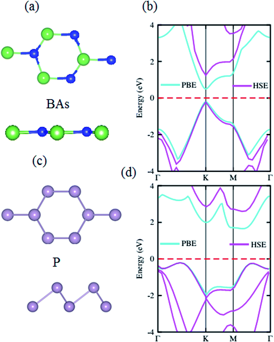 | ||
| Fig. 1 The atomic structures of the (a) BAs and (c) BlueP monolayers with different top and side views. The blue, green and cyan balls represent the B, As and P atoms, respectively. The calculated band structures of the (b) BAs and (d) BlueP monolayers by HSE06 and PBE methods. The red dashed line represents the Fermi level, which is set to zero. | ||
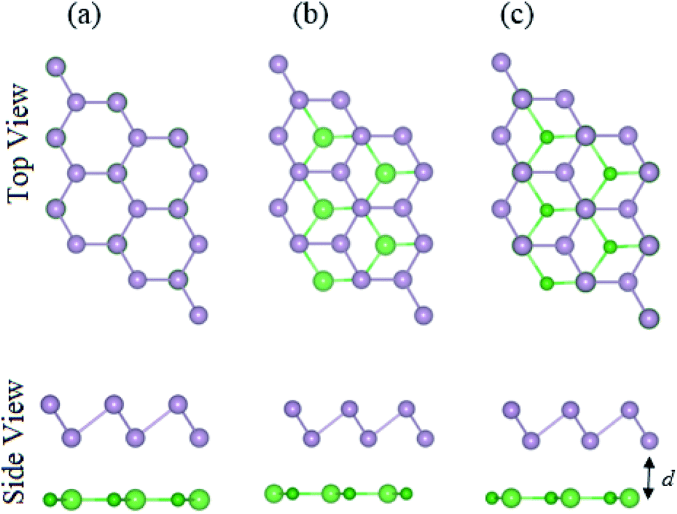
The atomic structures of the BAs–BlueP heterostructure with different stacking configurations, namely the AA, AB1 and AB2 patterns, are depicted in Fig. 2. In the AA stacking pattern, the P atoms are placed above the As and B atoms, as depicted in Fig. 2(a). In the AB1 stacking pattern, one P atom is stacked on the As atoms, and one P atom is centered in the hexagonal As–B ring, as depicted in Fig. 2(b). In the AB2 stacking pattern, one P atom is placed above a B atom and one other B atom is centered at the B–As hexagonal ring Fig. 2(c). After geometric optimization, the interlayer distances of BAs–BlueP for the AA, AB1 and AB2 stacking patterns are 3.39 Å, 3.42 Å and 3.16 Å, respectively. This implies that the AB2 stacking configuration of the BAs–BlueP heterostructure has the shortest interlayer distance compared with the others. Moreover, the calculated binding energies of the BAs–BlueP heterostructure for the AA, AB1 and AB2 patterns are −0.24 eV, −0.18 eV and −0.28 eV, respectively. The shortest interlayer distance and the smallest binding energy of the AB2 stacking pattern of the BAs–BlueP heterostructure confirm it as the most energetically favorable stacking pattern. Moreover, to check the thermal stability of this pattern, we further calculate the fluctuation of the total energy and temperature as a function of the heating time step by performing the ab initio molecular dynamics (AIMD) simulation. The thermal stability of this pattern is presented in Fig. 3. The atomic structure of the BAs–BlueP heterostructure before and after heating for 4 ps demonstrates that there is no distortion, confirming its structural stability. In addition, the fluctuation of total energy at 0 ps and 4 ps is small, indicating that it is thermally stable at room temperature.
 | ||
| Fig. 2 Top and side views of the atomic structures of the BAs–BlueP heterostructure with different stacking configurations: (a) AA pattern, (b) AB1 pattern and (c) AB2 pattern. | ||
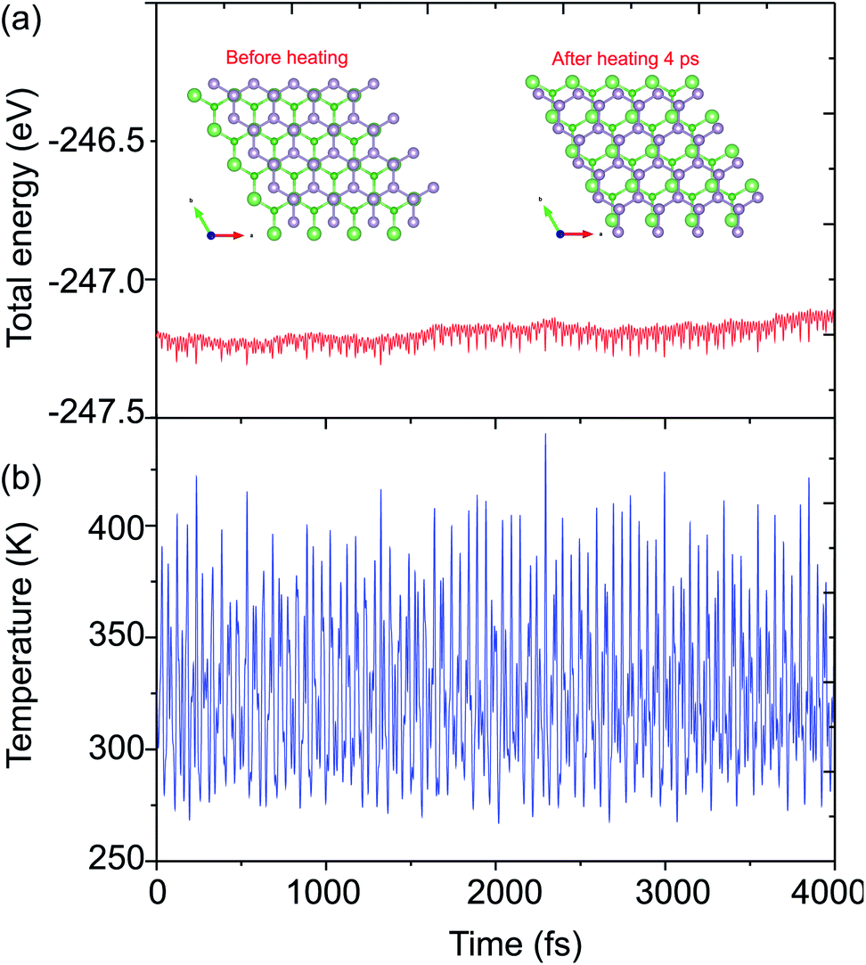 | ||
| Fig. 3 AIMD simulation of the fluctuation of the (a) total energy and (b) temperature as functions of the time step at 300 K for the BAs–BlueP heterostructure. The inset in (a) presents the diagrams of the atomic structure of the BAs–BlueP heterostructure before and after heating for 4 ps. | ||
The electronic band structure of the BAs–BlueP heterostructure is displayed in Fig. 4(a). The magenta lines represent the HSE06 bands and the green lines represent the VBM and CBM of this heterostructure using the PBE method. The BAs–BlueP heterostructure exhibits a semiconducting nature with a direct band gap. Both the VBM and CBM of this heterostructure appear at the K point using HSE06 and PBE calculations. The calculated band gap of the BAs–BlueP heterostructure is 0.56 eV and 1.31 eV from the PBE and HSE06 calculations, respectively. It is clear that the PBE method always underestimates the band gap, while the HSE06 can be used to correct this issue. It can be found that the value of the band gap of the BAs–BlueP heterostructure is smaller than those of the pristine BAs and BlueP monolayers. The reduction in the band gap of this heterostructure demonstrates that it will have a wider range of optical absorption in the visible region compared with the constituent monolayers.
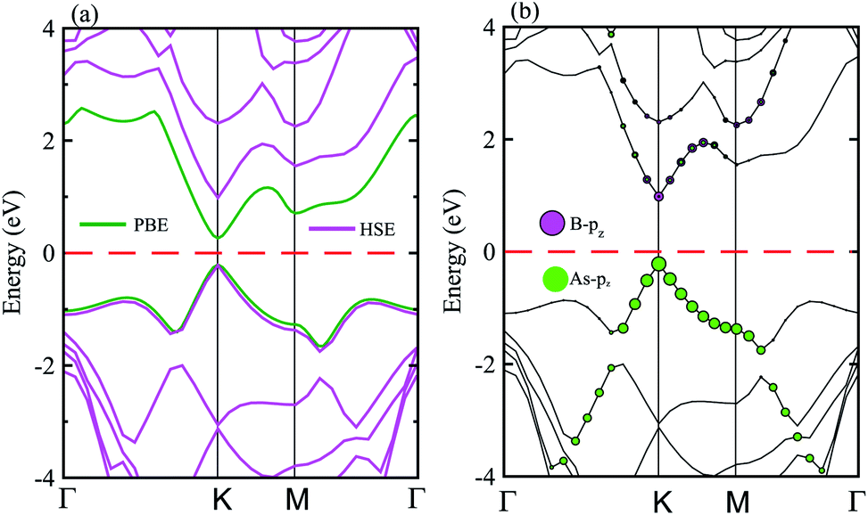 | ||
| Fig. 4 (a) Calculated band structure of the BAs–BlueP heterostructure using HSE and PBE calculations. (b) Weighted band structure of the BAs–BlueP heterostructure obtained from HSE06 calculations. | ||
Furthermore, it is well known that stacking 2D materials on top of each other gives rise to the formation of either type-I (straddling), type-II (staggered) or type-III (broken) band alignment. Therefore, to efficiently use this heterostructure for the design of high-performance nanodevices it is necessary to understand the formation of the band alignment. Fig. 4(b) depicts the weighted band structure of the BAs–BlueP heterostructure from HSE06 calculations. We find that both the VBM and CBM of this heterostructure are mainly contributed to by the BAs layer. This demonstrates that the BAs–BlueP heterostructure forms type-I (straddling gap) band alignment. The formation of the type-I straddling gap in the BAs–BlueP heterostructure may result in ultrafast electron–hole recombination, thus making it promising for light-emitting diodes due to the high emission efficiency.
The plane-averaged charge density difference of the BAs–BlueP heterostructure is presented in Fig. 5(a). It can be seen that the BAs layer has a positive charge, while the BlueP monolayer is negatively charged. This implies that the electrons are likely transferred from the BAs layer to the BlueP layer in the BAs/BlueP heterostructure. Bader charge analysis shows that a small amount of charge, 0.09 electrons, is transferred from the BAs layer to the BlueP layer. Moreover, the 3D isosurface of the charge redistribution at the interface is depicted in Fig. 5(c). It is evident that charges mainly accumulate in the BlueP layer, whereas they are depleted in the BAs layer, confirming the charge transportation from the BAs layer to the BlueP layer. It is noticeable that the charge redistribution at the interfacial region of this heterostructure may facilitate the separation of photo-excited electrons and holes and prolong carrier lifetimes, which is also revealed in excellent photocatalysts. The electrostatic potential along the z direction of the BAs–BlueP heterostructure is presented in Fig. 5(b), which shows a potential drop of 2.22 eV between the potentials of the BAs and BlueP layers. This potential drop gives rise to the formation of a strong internal electric field.
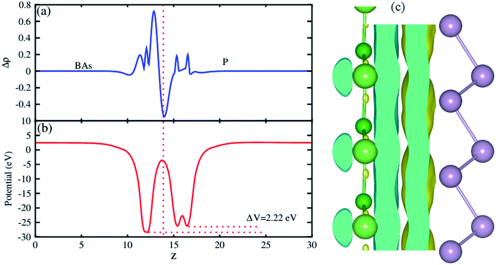 | ||
| Fig. 5 (a) The plane-averaged charge density differences, (b) the electrostatic potential and (c) the 3D isosurface of the charge density difference of the BAs/BlueP heterostructure. The isosurface value is set to 10−3 e Å−3. | ||
The optical properties of the BAs–BlueP heterostructure are established by calculating the imaginary part of the dielectric functions. The imaginary part of the dielectric functions of the constituent BAs and BlueP monolayers are also calculated for comparison. The BAs–BlueP heterostructure possesses type-I straddling band alignment, thus, the optical transition between the two layers is due to the interlayer recombination of the electrons and holes. One can see in Fig. 6 that the first peak in the imaginary part of the heterostructure comes from the BlueP monolayer. Moreover, this peak appears at a lower energy than that of the BlueP monolayer, indicating the reduction in the optical band gap of the heterostructure.
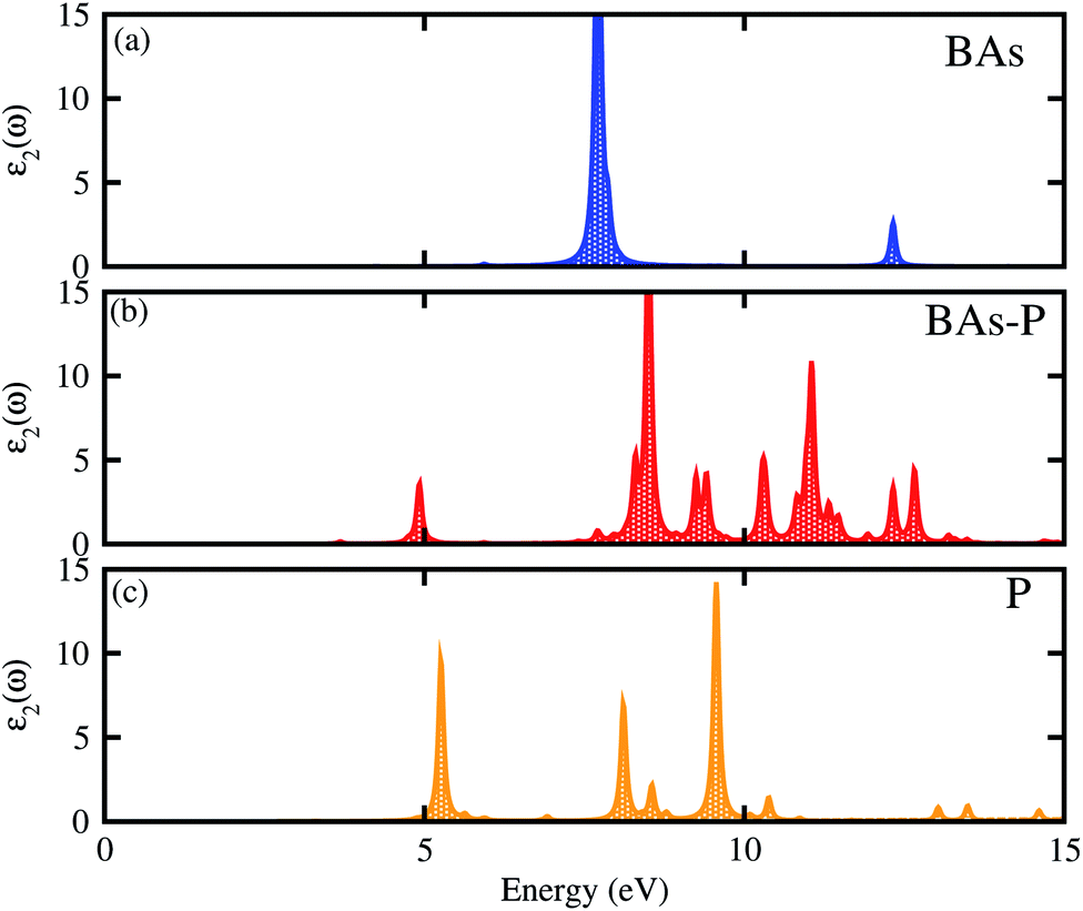 | ||
| Fig. 6 Calculated imaginary parts of the dielectric functions as a function of photon energy for (a) isolated BAs, (b) the BAs–BlueP heterostructure and (c) the BlueP monolayer. | ||
Next, we investigate the photocatalytic performance of the BAs and BlueP monolayers as well as their corresponding heterostructure using Mulliken electronegativity and the valence and conduction band edge potentials as follows:
| EVBM = χ − Ee + 0.5Eg | (3) |
| ECBM = χ − Ee − 0.5Eg | (4) |
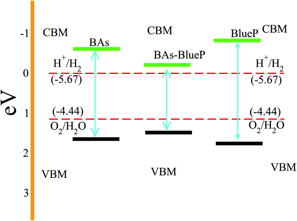 | ||
| Fig. 7 Calculated band edge alignments of the BAs–BlueP heterostructure as well as the corresponding constituent monolayers. The red dashed lines represent the redox potentials for water splitting at pH = 0. | ||
4 Conclusion
In summary, we investigated the structural, electronic, optical and photocatalytic properties of BAs and BlueP monolayers and their corresponding heterostructure using density functional theory. Our results reveal that both BAs and BlueP monolayers exhibit the direct band gaps of a semiconductor, whereas the formation of the BAs–BlueP vdW heterostructure results in type-I band-alignment with a direct band gap. The formation of the type-I straddling gap in the BAs–BlueP heterostructure may result in ultrafast electron–hole recombination. Furthermore, one can find that the BAs layer donates electrons to the BlueP layer, resulting in the formation of p-doping in the BAs layer and n-doping in the BlueP layer. The optical absorption spectrum shows that the first peaks are dominated by excitons. Moreover, the BAs–BlueP heterostructure is a good material for water splitting at pH = 0.Conflicts of interest
The authors declare that there are no conflicts of interest regarding the publication of this paper.References
- Y. Zhong, Z. Zhen and H. Zhu, FlatChem, 2017, 4, 20–32 CrossRef CAS.
- D. A. Brownson, D. K. Kampouris and C. E. Banks, J. Power Sources, 2011, 196, 4873–4885 CrossRef CAS.
- A. C. Neto, F. Guinea, N. M. Peres, K. S. Novoselov and A. K. Geim, Rev. Mod. Phys., 2009, 81, 109 CrossRef.
- X. Fan, Z. Shen, A. Liu and J.-L. Kuo, Nanoscale, 2012, 4, 2157–2165 RSC.
- P. Rani and V. Jindal, RSC Adv., 2013, 3, 802–812 RSC.
- F. Guinea, M. Katsnelson and A. Geim, Nat. Phys., 2010, 6, 30–33 Search PubMed.
- C. Si, Z. Sun and F. Liu, Nanoscale, 2016, 8, 3207–3217 RSC.
- S. Manzeli, D. Ovchinnikov, D. Pasquier, O. V. Yazyev and A. Kis, Nat. Rev. Mater., 2017, 2, 17033 CrossRef CAS.
- Q. H. Wang, K. Kalantar-Zadeh, A. Kis, J. N. Coleman and M. S. Strano, Nat. Nanotechnol., 2012, 7, 699–712 CrossRef CAS PubMed.
- D. Jariwala, V. K. Sangwan, L. J. Lauhon, T. J. Marks and M. C. Hersam, ACS Nano, 2014, 8, 1102–1120 CrossRef CAS PubMed.
- M. Z. Rahman, C. W. Kwong, K. Davey and S. Z. Qiao, Energy Environ. Sci., 2016, 9, 709–728 RSC.
- H. Liu, A. T. Neal, Z. Zhu, Z. Luo, X. Xu, D. Tománek and P. D. Ye, ACS Nano, 2014, 8, 4033–4041 CrossRef CAS PubMed.
- E. S. Reich, et al., Nature, 2014, 506, 19 CrossRef PubMed.
- M. Naguib, V. N. Mochalin, M. W. Barsoum and Y. Gogotsi, Adv. Mater., 2014, 26, 992–1005 CrossRef CAS PubMed.
- J. Zhu, E. Ha, G. Zhao, Y. Zhou, D. Huang, G. Yue, L. Hu, N. Sun, Y. Wang and L. Y. S. Lee, et al., Coord. Chem. Rev., 2017, 352, 306–327 CrossRef CAS.
- B. Anasori, M. R. Lukatskaya and Y. Gogotsi, Nat. Rev. Mater., 2017, 2, 1–17 Search PubMed.
- J. Zheng, E. Li, Z. Cui and D. Ma, Phys. E., 2020, 124, 114277 CrossRef CAS.
- J. Li, Z. Huang, W. Ke, J. Yu, K. Ren and Z. Dong, J. Alloys Compd., 2021, 866, 158774 CrossRef CAS.
- Z. Guan, C.-S. Lian, S. Hu, S. Ni, J. Li and W. Duan, J. Phys. Chem. C, 2017, 121, 3654–3660 CrossRef CAS.
- H. Shu, Mater. Sci. Eng., B, 2020, 261, 114672 CrossRef CAS.
- H. Shu, Y. Wang and M. Sun, Phys. Chem. Chem. Phys., 2019, 21, 15760–15766 RSC.
- H. Shu, J. Guo and X. Niu, J. Mater. Sci., 2019, 54, 2278–2288 CrossRef CAS.
- K. Ren, J. Yu and W. Tang, J. Alloys Compd., 2020, 812, 152049 CrossRef CAS.
- H. Shu, Mater. Adv., 2020, 1, 1849–1857 RSC.
- M. Xie, S. Zhang, B. Cai, Z. Zhu, Y. Zou and H. Zeng, Nanoscale, 2016, 8, 13407–13413 RSC.
- R. Sheng, X. Deng, Z. Zhang and Z. Fan, Phys. Lett. A, 2020, 384, 126150 CrossRef CAS.
- H. Ye, H. Sheng, D. Bai, J. Zhang and J. Wang, Phys. E., 2020, 120, 114055 CrossRef CAS.
- A. A. Attia and H. R. Jappor, Chem. Phys. Lett., 2019, 728, 124–131 CrossRef CAS.
- J. L. Zhang, S. Zhao, C. Han, Z. Wang, S. Zhong, S. Sun, R. Guo, X. Zhou, C. D. Gu and K. D. Yuan, et al., Nano Lett., 2016, 16, 4903–4908 CrossRef CAS PubMed.
- V. Tran, R. Soklaski, Y. Liang and L. Yang, Phys. Rev. B: Condens. Matter Mater. Phys., 2014, 89, 235319 CrossRef.
- M. Sun, J.-P. Chou, A. Hu and U. SchwingenschloÌĹgl, Chem. Mater., 2019, 31, 8129–8135 CrossRef CAS.
- J. Zhuang, C. Liu, Q. Gao, Y. Liu, H. Feng, X. Xu, J. Wang, J. Zhao, S. X. Dou and Z. Hu, et al., ACS Nano, 2018, 12, 5059–5065 CrossRef CAS PubMed.
- J. Xiao, M. Long, C.-S. Deng, J. He, L.-L. Cui and H. Xu, J. Phys. Chem. C, 2016, 120, 4638–4646 CrossRef CAS.
- G. Kresse and J. Furthmüller, Comput. Mater. Sci., 1996, 6, 15–50 CrossRef CAS.
- J. P. Perdew, K. Burke and M. Ernzerhof, Phys. Rev. Lett., 1996, 77, 3865 CrossRef CAS PubMed.
- P. E. Blöchl, Phys. Rev. B: Condens. Matter Mater. Phys., 1994, 50, 17953 CrossRef PubMed.
- J. Heyd, G. E. Scuseria and M. Ernzerhof, J. Chem. Phys., 2003, 118, 8207–8215 CrossRef CAS.
- A. V. Krukau, O. A. Vydrov, A. F. Izmaylov and G. E. Scuseria, J. Chem. Phys., 2006, 125, 224106 CrossRef PubMed.
- I. Shahid, S. Ahmad, N. Shehzad, Y. Sai, C. V. Nguyen, L. Zhang and Z. Zhou, Appl. Surf. Sci., 2020, 523, 146483 CrossRef CAS.
| This journal is © The Royal Society of Chemistry 2021 |