
 Open Access Article
 This Open Access Article is licensed under a Creative Commons Attribution-Non Commercial 3.0 Unported Licence
Studies on the substrate-dependent photocatalytic properties of Cu2O heterojunctions†
Riza Ariyani Nur Khasanah a,
Hui-Ching Lina,
Hsiang-Yun Hob,
Yen-Ping Pengc,
Tsong-Shin Lima,
Hsi-Lien Hsiaoa,
Chang-Ren Wanga,
Min-Chieh Chuangd and
Forest Shih-Sen Chien*a
a,
Hui-Ching Lina,
Hsiang-Yun Hob,
Yen-Ping Pengc,
Tsong-Shin Lima,
Hsi-Lien Hsiaoa,
Chang-Ren Wanga,
Min-Chieh Chuangd and
Forest Shih-Sen Chien*a
aDepartment of Applied Physics, Tunghai University, Taichung 407224, Taiwan. E-mail: fsschien@thu.edu.tw
bDepartment of Environmental Science and Engineering, Tunghai University, Taichung 407224, Taiwan
cInstitute of Environmental Engineering, National Sun Yat-sen University, Kaoshiung 804, Taiwan
dDepartment of Chemistry, Tunghai University, Taichung 407224, Taiwan
First published on 26th January 2021
Abstract
Cu2O is a promising material for photocatalysis because of its absorption ability in the ultraviolet (UV)-visible light range. Cu2O deposited on conductive Ti and fluorine-doped tin oxide (FTO) substrates behaves as a photocathode. Cu2O deposited on an n-type semiconductor such as TiO2 nanotube arrays (TNA)/Ti behaves as a photoanode and has demonstrated better photocatalytic activity than that of TNA/Ti. The substrate-dependent photocatalytic properties of Cu2O heterojunctions are not well studied. In this work, the photocatalytic properties of a Cu2O/TNA/Ti junction as a photoanode and of Cu2O/Ti and Cu2O/FTO junctions as photocathodes without bias were systematically studied to understand their performance. The Cu2O/TNA/Ti photoanode exhibited higher photocurrent spectral responses than those of Cu2O/Ti and Cu2O/FTO photocathodes. The photoanodic/photocathodic properties of those junctions were depicted in their energy band diagrams. Time-resolved photoluminescence indicated that Cu2O/TNA/Ti, Cu2O/Ti, and Cu2O/FTO junctions did not enhance the separation of photogenerated charges. The improved photocatalytic properties of Cu2O/TNA/Ti compared with TNA/Ti were mainly attributed to the UV-visible light absorption of Cu2O.
1. Introduction
Metal oxide semiconductors have attracted extensive interest because they are potentially low cost and environmentally friendly materials for photocatalytic applications. Cuprous oxide (Cu2O), one of the metal oxide p-type semiconductors, has a direct band gap energy between 2.0 eV and 2.6 eV.1,2 At pH = 7.0, its conduction band (−1.35 V vs. Ag/AgCl) lies at more negative potential than the reduction potential of H+ to H2 (−0.61 V vs. Ag/AgCl), and its valence band (0.65 V vs. Ag/AgCl) lies at more positive potential than the oxidation potential of H2O to O2 (0.62 V vs. Ag/AgCl).3,4 Cu2O is able to absorb ultraviolet (UV)-visible light and has some tremendous characteristics, such as nontoxic nature, abundant availability, and low fabrication cost.5 With the appropriate positioning of energy bands and these advantages, Cu2O is a potential candidate for photocatalyst that can generate H2 through water splitting and degrade organic pollutants in wastewater.6–8 Cu2O behaves as a catalyst under dark conditions and photocathode under illumination.4,9 Typically, Cu2O is grown on conductive substrates, such as Cu,10 Ti,11,12 Al,10 fluorine-doped tin oxide (FTO),12–14 and indium tin oxide (ITO),4,13 and can still behave as a photocathode.To further advance this promising photocatalytic material, Cu2O has been used as top layers on various n-type metal oxide semiconductors, such as TiO2,15 ZnO,16 WO,3,17 and g-C3N4,18 to form heterojunctions and enhance photogenerated charge separation. These junctions demonstrate better photocatalytic activity than that of bare Cu2O. Cu2O combined with TiO2 is an attractive composite because of its matching energy-level alignments that thermodynamically promoting the transfer of photogenerated electrons from Cu2O to TiO2.19 TiO2 is the most popular n-type metal oxide semiconductor in photocatalysis, that has a wide band gap energy (approximately 3.0 eV for rutile20 and 3.2 eV for anatase21) and several beneficial characteristics, such as chemical stability, corrosion resistance, environmental friendliness, abundance, and cost effectiveness.22 However, the solar energy conversion efficiency of TiO2 is limited by UV light absorption. To date, TiO2 nanotube arrays (TNA)/Ti has been favoured because of its higher surface-area-to-volume ratio.23,24 Cu2O electrodeposited on TNA/Ti (Cu2O/TNA/Ti) has been applied in the photocatalytic degradation of pollutants, such as methyl orange (dye),25 CO2 (gas),26 ibuprofen (drug),27,28 and ciprofloxacin (drug).29 To this end, Cu2O/TNA/Ti is more effective than TNA/Ti. Contrary to the Cu2O-functionalized conductive substrates, which are utilized as photocathodes, Cu2O/TNA/Ti frequently acts as a photoanode. However, the substrate-dependent photocatalytic properties of p-Cu2O heterojunctions are not well studied, and the heterojunctions are a critical issue in photocatalysis. Moreover, the Cu2O/TNA heterojunction is very important for photocatalysis. It is considered that the heterojunction enhance the separation of photogenerated charges.25–29 In fact, the enhancement of the charge separation at Cu2O/TNA junction to assist in photocatalysis has yet to be verified.
In this study, the photocatalytic properties of Cu2O/TNA/Ti were compared with those of Cu2O/Ti and Cu2O/FTO. A p-Cu2O was deposited on different substrates, i.e., n-TNA/Ti, Ti, and n-FTO. The results revealed that the Cu2O/TNA/Ti photoanode exhibited higher photocurrent spectral responses, which obviously outperformed the Cu2O/Ti and Cu2O/FTO photocathodes. The photoanodic current of Cu2O/TNA/Ti was twice as high as that of TNA/Ti. The higher photocatalytic performance of Cu2O/TNA/Ti over other junctions was verified by the degradation of rhodamine 6G (R6G). The results of time-resolved photoluminescence (TRPL) for both the TNA and Cu2O sides of Cu2O/TNA/Ti revealed that the junction of Cu2O/TNA did not enhance the charge separation. Both Cu2O/Ti and Cu2O/FTO did not enhance the charge separation from TRPL measurement, either. The improved photocatalytic properties of the Cu2O/TNA/Ti over TNA/Ti alone were mainly ascribed to the UV-visible light absorption of Cu2O.
2. Results and discussion
2.1 Morphology, crystalline phase, and optical absorption
The morphologies of TNA/Ti, Cu2O/TNA/Ti, Cu2O/Ti, and Cu2O/FTO are shown in Fig. 1. A nanotube morphology of TNA with an outer diameter of approximately 90 nm could be clearly observed, as depicted in Fig. 1(a). The cross-sectional image in the inset demonstrates that TNA was vertically well-aligned on Ti, with a length of approximately 2 μm. Fig. 1(b) shows that the morphology of Cu2O on TNA surface exhibited an octahedral shape with a side length of approximately 430 nm and a coverage of 25%. The structures of TNA retained their integrity without significant change after the deposition of Cu2O. Cu2O on Ti had an octahedral shape, with a side length of approximately 380 nm and total coverage of 50% [Fig. 1(c)]. Similarly, Cu2O on FTO had an octahedral shape, with a side length of approximately 500 nm and total coverage of 60% [Fig. 1(d)]. However, some aggregations of Cu2O were observed on the Ti and FTO surfaces. During the electrodeposition of Cu2O, the conductivity of the substrate critically affected the morphology of the deposited Cu2O.13,30 Obviously, there were significant differences in the sheet resistance among TNA, FTO, and Ti, which were 2.64 ± 0.15 MΩ sq−1, 7.86 ± 0.04 Ω sq−1, and 1.66 ± 0.04 mΩ sq−1, respectively.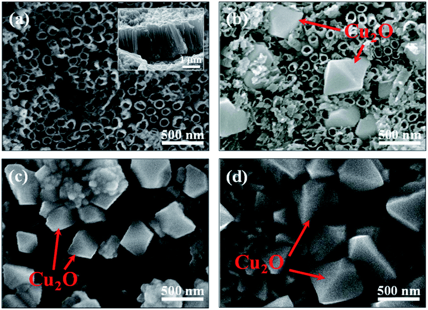 | ||
| Fig. 1 Top-view scanning electron microscopy (SEM) images of (a) TNA/Ti, (b) Cu2O/TNA/Ti, (c) Cu2O/Ti, and (d) Cu2O/FTO. The inset in (a) is the cross-sectional SEM image of TNA/Ti. | ||
The X-ray diffraction (XRD) patterns in Fig. 2(a) display peaks confirming the presence of Ti, TNA, Cu2O, and FTO. The TNA/Ti and Cu2O/TNA/Ti had peaks with 2θ values of 25.34°, 37.98°, 48.10°, and 54.10°, which were indexed to the (101), (004), (200), and (105) crystal planes of anatase TiO2 (ICSD file no. 98-007-6028), respectively. Two peaks with 2θ values of 36.58° and 42.29°, observed on Cu2O/TNA/Ti, Cu2O/Ti, and Cu2O/FTO, were indexed to the (111) and (200) crystal planes of Cu2O (ICSD file no. 98-006-0719), respectively. No Cu or CuO peaks were observed in Cu2O/TNA/Ti, Cu2O/Ti, or Cu2O/FTO, indicating that only Cu2O was grown in the substrates. For comparison, the morphology and XRD pattern of the commercial Cu2O are also presented in Fig. S1.† The optical absorption spectra of TNA/Ti, Cu2O/TNA/Ti, Cu2O/Ti, and Cu2O/FTO are shown in Fig. 2(b). TNA/Ti demonstrated high absorption in the UV region, with an approximate band gap energy of 3.35 eV (370 nm), which is consistent with the anatase phase.31 Broad light scattering of TNA/Ti caused by its specific structure was observed in the visible region.32 Cu2O/TNA/Ti, Cu2O/Ti, and Cu2O/FTO all demonstrated a visible light absorption edge at 500 nm due to the band gap of Cu2O (2.47 eV), which is consistent with values reported in other studies.1,2 The additional absorption edge at 560 nm observed in Cu2O/Ti is attributable to the absorption characteristics of Ti. The absorption characteristics of Cu2O/FTO were obtained through measurement of the reflection and transmission spectra, as shown in Fig. S2.† The optical absorption of the commercial Cu2O is shown in Fig. S3.†
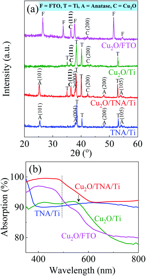 | ||
| Fig. 2 (a) XRD patterns and (b) optical absorption spectra of TNA/Ti, Cu2O/TNA/Ti, Cu2O/Ti, and Cu2O/FTO. The dashed line indicates the absorption edge of Cu2O. An arrow denotes the additional absorption due to Ti. | ||
2.2 Photocatalytic properties
Fig. 3 shows the spectral response with the working electrodes of Cu2O/TNA/Ti, Cu2O/Ti, Cu2O/FTO, and TNA/Ti, which were obtained from the photocurrent intensity under different monochromatic wavelengths, with a light intensity of 5 mW cm−2 (Fig. S4†). With positive spectral responses, TNA/Ti and Cu2O/TNA/Ti are photoanodes, and with negative spectral responses, Cu2O/Ti and Cu2O/FTO are photocathodes. TNA/Ti exhibited a high response to UV light (10.1 μA mW−1 at 365 nm and 1.8 μA mW−1 at 385 nm) but a low response to visible light (0.21 μA mW−1 at 415 nm). The responses of Cu2O/TNA/Ti in the UV-visible region (4.0 μA mW−1 at 385 nm and 2.2 μA mW−1 at 415 nm) were approximately 2 and 10 times larger than that of TNA/Ti, and the onset of response at 590 nm (0.16 μA mW−1) was consistent with the onset of absorption in Fig. 2(b). This higher spectral response observed in Cu2O/TNA/Ti could be attributed to the absorption of Cu2O, which is active in the UV-visible range. Cu2O/Ti and Cu2O/FTO also had the same onset of response (shown in the inset of Fig. 3), but their overall responses were low, indicating that Cu2O is a poor photocathode.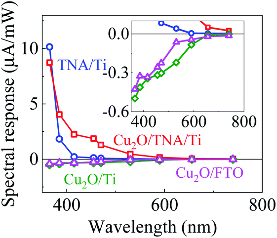 | ||
| Fig. 3 Spectral responses of TNA/Ti, Cu2O/TNA/Ti, Cu2O/Ti, and Cu2O/FTO. The inset is the enlarge graph to see the onset response of Cu2O/Ti and Cu2O/FTO. | ||
The photocurrent density was measured under a solar simulator. Under dark conditions, both Cu2O/TNA/Ti and TNA/Ti exhibited no current density. Under solar light (λ > 350 nm), Cu2O/TNA displayed a photocurrent density of 27 μA cm−2, approximately twice that of TNA/Ti (15 μA cm−2) [Fig. 4(a)]. Under visible light (λ > 400 nm), Cu2O/TNA/Ti demonstrated a photocurrent density of 14 μA cm−2, whereas TNA/Ti had a low photocurrent density (2 μA cm−2) [Fig. 4(b)]. Fig. 4(c) presents the photovoltage obtained from the open-circuit potential (OCP) vs. Ag/AgCl, which is directly related to the photocurrent. Under dark conditions, the OCPs of TNA/Ti and Cu2O/TNA/Ti were 0.1 V vs. Ag/AgCl. Subsequently, a negative photovoltage was observed when the working electrode was illuminated by solar light. A negative photovoltage indicates that electrons accumulated in the electrodes, denoting a photoanode. Cu2O/TNA/Ti had a more negative photovoltage (−0.17 V vs. Ag/AgCl) compared with that of TNA/Ti (−0.13 V vs. Ag/AgCl), indicating that a greater number of electrons accumulated in the Cu2O/TNA/Ti upon illumination. The photocurrent densities of Cu2O/Ti and Cu2O/FTO under solar light in Fig. 4(d) and visible light in Fig. 4(e) demonstrate the typical behaviour of p-type semiconductors to be photocathodes. The photocurrent densities of Cu2O/Ti and Cu2O/FTO under solar light were approximately −3.0 μA cm−2 and −4.0 μA cm−2, respectively. Under visible light, Cu2O/Ti and Cu2O/FTO exhibited photocurrent densities of −2.4 μA cm−2 and −3.1 μA cm−2, respectively. Fig. 4(f) shows OCPs vs. Ag/AgCl under solar light, which fluctuated between 0.05 V and 0.08 V and between 0.04 V and 0.09 V for Cu2O/Ti and Cu2O/FTO, respectively. The positive photovoltages suggest that holes accumulated in the working electrodes.
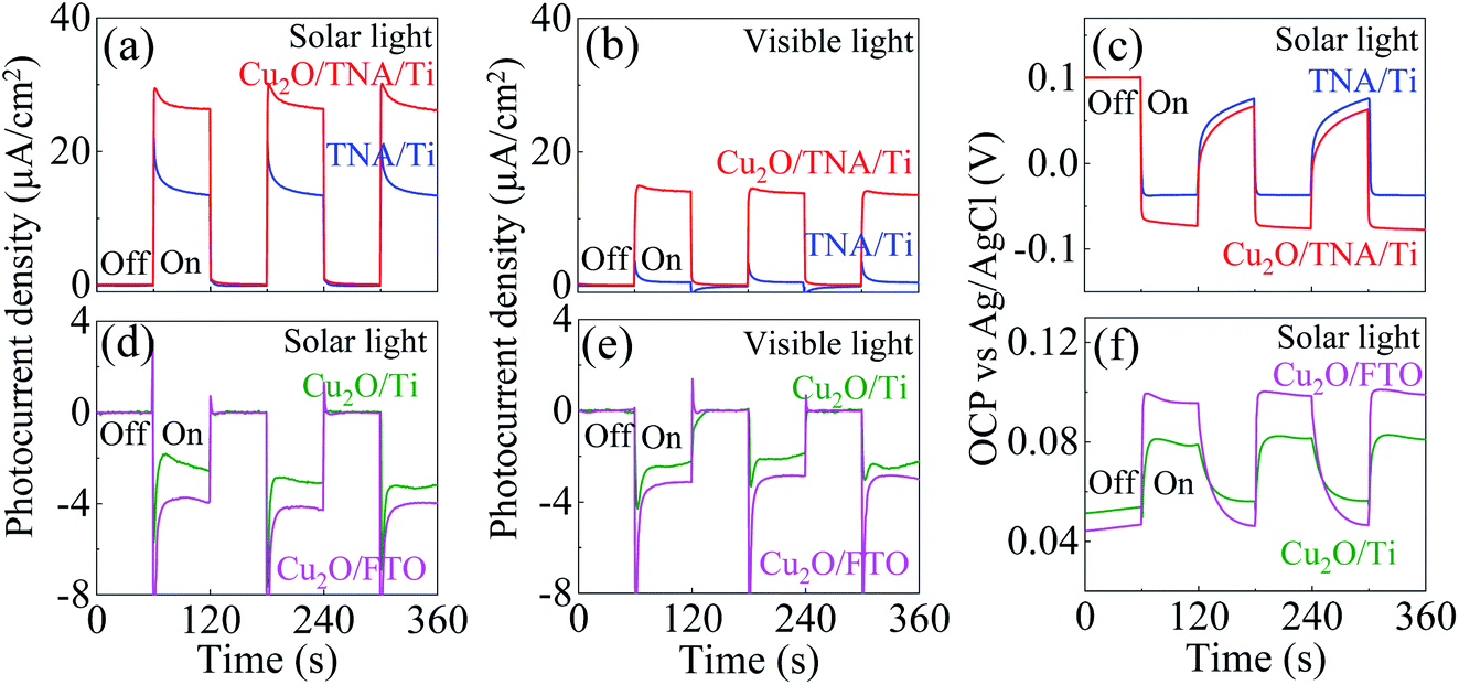 | ||
| Fig. 4 (a and b) Photocurrent density of TNA/Ti and Cu2O/TNA/Ti under solar light and visible light. (c) OCP vs. Ag/AgCl of TNA/Ti and Cu2O/TNA/Ti under solar light. (d and e) Photocurrent density of Cu2O/Ti and Cu2O/FTO under solar light and visible light. (f) OCP vs. Ag/AgCl of Cu2O/Ti and Cu2O/FTO under solar light. | ||
The photocatalytic activity of Cu2O/TNA/Ti, Cu2O/Ti, Cu2O/FTO, and TNA/Ti was evaluated though the degradation of R6G under solar light without bias through monitoring of the change in height of the absorption peak at a wavelength of 527 nm.33 R6G was degraded through photooxidation process. Fig. 5(a) shows the decrease of the absorption spectra of R6G degraded by the photocatalysis with Cu2O/TNA/Ti. Fig. 5(b) presents the photocatalytic degradation in the R6G concentration with different working electrodes. Cu2O/TNA/Ti could degrade R6G by approximately 55% in 120 min. However, TNA/Ti, Cu2O/Ti, and Cu2O/FTO demonstrated smaller degradation effects on R6G than that of Cu2O/TNA/Ti, with approximate degradation percentages of 30%, 26%, and 25%, respectively. Hence, the photooxidation of R6G is favourable with the Cu2O/TNA/Ti photoelectrode.
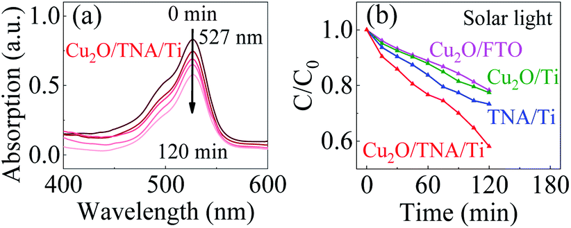 | ||
| Fig. 5 (a) Decrement of the R6G absorption peak by Cu2O/TNA/Ti under solar light. (b) Degradation of the R6G concentration (C/C0) by Cu2O/TNA/Ti, Cu2O/Ti, Cu2O/FTO, and TNA/Ti under solar light. | ||
2.3 Energy band diagram of Cu2O heterojunctions
The photocatalytic behaviours (photoanode or photocathode) of TNA/Ti, Cu2O/TNA/Ti, Cu2O/Ti, and Cu2O/FTO can be described by their energy band diagrams obtained upon light illumination (Fig. 6). In a state of equilibrium under dark conditions, a Schottky junction formed at the TNA/Ti interface with a built-in potential (Vbi) of approximately 0.27 V,34 as shown in Fig. 6(a). When TNA absorbed UV light, electrons and holes were generated at the conduction and valence bands, respectively. The photogenerated electrons were transferred to the Ti back contact and then moved to Pt through an external circuit; subsequently, the photogenerated holes were transferred to the Na2SO4 electrolyte as a photoanodic current. Cu2O/TNA created a staggered-gap (Type II) heterojunction with a built-in potential (Vbi) of 0.89 V,34 as shown in Fig. 6(b). Cu2O/TNA/Ti behaved as a photoanode analogous to TNA/Ti.27,29 Cu2O absorbed UV-visible light and generated electron–hole pairs. The photogenerated electrons in the conduction band of Cu2O were transferred to the conduction band of TNA and then to the Ti back contact, and photogenerated holes in the valence band of TNA were transferred to the valence band of Cu2O and then to the Na2SO4 electrolyte, serving as a photoanodic current. As seen in Fig. 3, the response of TNA/Ti at 365 nm was higher than that of Cu2O/TNA/Ti, which indicates the TNA/Ti is favourable to the transfer of photoelectrons. In addition, in Fig. 4(a), the photocurrent of TNA/Ti under solar light was almost half the photocurrent of Cu2O/TNA/Ti, thought that TNA/Ti only takes UV light, which is less than 10% of the solar power. Therefore the charge transfer at Cu2O/TNA is more difficult than that at TNA/Ti; the effect of TNA/Ti can be insignificant.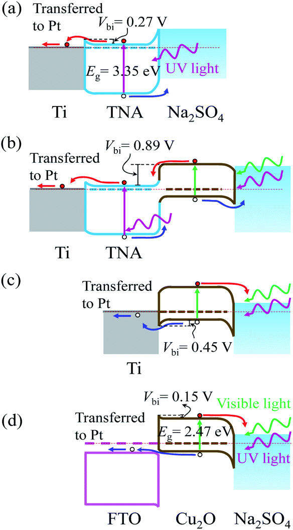 | ||
| Fig. 6 Energy band diagrams involving (a) TNA/Ti, (b) Cu2O/TNA/Ti, (c) Cu2O/Ti, and (d) Cu2O/FTO in the Na2SO4 0.05 M electrolyte upon light illumination without applied bias. | ||
Cu2O/Ti formed a Schottky junction with a built-in potential (Vbi) of approximately 0.45 V,34 as displayed in Fig. 6(c). When Cu2O absorbed UV-visible light, a photocathodic current was observed because the photogenerated holes were easily transferred to the Ti back contact, and the photogenerated electrons were transferred to the Na2SO4 electrolyte. Furthermore, FTO is an n-type degenerate semiconductor, but behaves like a metal14 and has a Fermi level above the conduction band,35 as indicated in Fig. 6(d). The work function of Cu2O is a little lower than that of FTO. At equilibrium state, Cu2O/FTO created a broken-gap (type III) junction, yielding a band bending that demonstrated an ohmic contact36 for hole transfer and a small barrier for electron transfer to FTO with a built-in potential (Vbi) of approximately 0.15 V. Similar to the case for Cu2O/Ti, the photogenerated holes of Cu2O were transferred to the conduction band of FTO and further transferred to Pt through an external circuit, whereas the photogenerated electrons were transferred to the Na2SO4 electrolyte. Hence, a photocathodic current was observed.
2.4 Charge lifetime of photogenerated charges
It is a common belief that the built-in potential could lead to charge separation enhancement at the Cu2O/TNA junction, where the photogenerated electrons in the conduction band of Cu2O to drift toward the conduction band of TNA and the photogenerated holes in the valence band of TNA to drift toward the valence band of Cu2O.25–29 Enhanced charge separation created in the junction can reduce the probability of electron–hole recombination and enhance photocatalysis. To understand the presence of charge separation enhancement at the Cu2O/TNA junction, photoluminescence (PL) and TRPL of all samples were applied.The commercial Cu2O, bare TNA/Ti, Cu2O/TNA/Ti, Cu2O/Ti, and Cu2O/FTO samples were excited by a 355 nm pulse laser under a long-pass filter (λ > 480 nm) and integration time of 1 s at room temperature to measure the PL, as shown in Fig. 7(a and b). Commercial Cu2O exhibited PL peaks located at 620 nm and 900 nm, which is attributable to the band-to-band transition of Cu2O and the defect states of copper vacancies.37,38 TNA/Ti exhibited broad band PL with a peak located at 600 nm, which is consistent with the reports of other studies.39,40 No PL of the band-to-band transition of TNA was observed because TNA is an indirect band gap semiconductor.39 The 500 nm and 600 nm broad band PL of TNA originated from surface oxygen vacancies and subsurface oxygen vacancies, respectively.40 The PL of TNA and Cu2O in the Cu2O/TNA/Ti sample was captured from the TNA and Cu2O sides (an integration time of 30 s was used to measure the PL of the Cu2O side because of the weak intensity). The Cu2O side of Cu2O/TNA/Ti, Cu2O/Ti, and Cu2O/FTO exhibited a broad band PL peak at 600 nm, mainly caused by band-to-band emission. Cu2O also had defects due to oxygen vacancies with +2 and +1 charge states at 770 nm and 825 nm, respectively, and copper vacancies at 900 nm.38 The TNA side demonstrated similar PL emission to that of bare TNA/Ti.
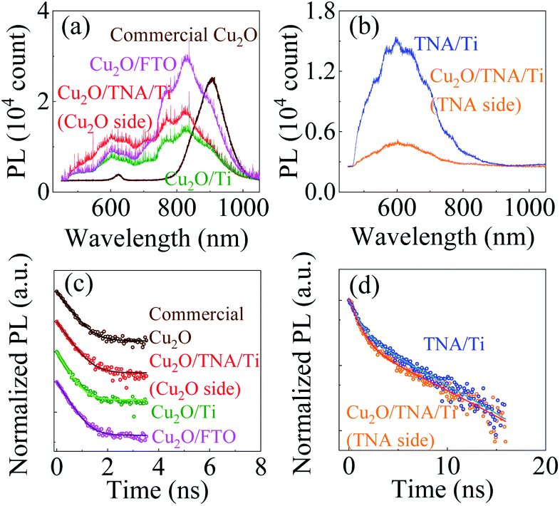 | ||
| Fig. 7 (a and b) PL spectra of commercial Cu2O, Cu2O/TNA/Ti (Cu2O and TNA sides), Cu2O/Ti, Cu2O/FTO, and TNA/Ti excited at a wavelength of 355 nm. (c) TRPL of the commercial Cu2O, Cu2O side of Cu2O/TNA/Ti, Cu2O/Ti, and Cu2O/FTO measured using a band-pass filter (600 nm/45 nm). The curves were shifted vertically for clarity. (d) TRPL of TNA/Ti and TNA side of Cu2O/TNA/Ti measured using a long-pass filter (λ > 480 nm). The TRPL results are plotted in the log scale. The solid lines in (c and d) are the fitting lines. | ||
The charge dynamics of the photogenerated charges was further studied by TRPL. Fig. 7(c) shows the TRPL of commercial Cu2O, Cu2O side of Cu2O/TNA/Ti, Cu2O/Ti, and Cu2O/FTO under a band-pass filter (600 nm ± 45 nm) because only the band-to-band transition of Cu2O was considered. Fig. 7(d) shows the TRPL of defect states in bare TNA/Ti and on the TNA side of Cu2O/TNA/Ti under a long-pass filter (λ > 480 nm). The TRPL results were fitted by a one-exponential-decay function for commercial Cu2O, Cu2O side of Cu2O/TNA/Ti, Cu2O/Ti, and Cu2O/FTO, and a two-exponential-decay function for bare TNA/Ti and TNA side of Cu2O/TNA/Ti, where τ1 and τ2 are the lifetimes of charge carriers along with the corresponding amplitudes, A1 and A2. The fitted results are summarized in Table 1. There is no significant difference of charge carrier lifetimes among commercial Cu2O (0.38 ns), Cu2O side of Cu2O/TNA/Ti (0.36 ns), Cu2O/Ti (0.31 ns), and Cu2O/FTO (0.33 ns), and between TNA/Ti (0.88 ns) and TNA side of Cu2O/TNA/Ti (0.86 ns). Thus, the Cu2O/TNA junction did not enhance the charge separation of photogenerated charges on the Cu2O or TNA sides. Therefore, no charge separation enhancement was observed at the Cu2O/TNA junction, which could be attributed to a poor contact area and poor quality of the Cu2O/TNA.
| TRPL | Cu2O side | TNA side | ||||
|---|---|---|---|---|---|---|
| Sample/parameter | Commercial Cu2O | Cu2O/TNA/Ti | Cu2O/Ti | Cu2O/FTO | TNA/Ti | Cu2O/TNA/Ti |
| A1 | 0.98 | 0.97 | 0.97 | 0.99 | 0.66 | 0.84 |
| τ1 (ns) | 0.38 | 0.36 | 0.31 | 0.33 | 0.88 | 0.86 |
| A2 | 0.35 | 0.23 | ||||
| τ2 (ns) | 5.24 | 5.90 | ||||
Inevitably, the contact area between the three-dimensional structures of TNA and the octahedral crystal grains of Cu2O prepared by square wave voltammetry electrochemical (SWVE) was remarkably small. The grain size of Cu2O was larger than the outer diameter of the TNA, as seen in Fig. 1(b). Such large grains of Cu2O were due to the high growth rate of Cu2O and resulted in the low contact area and low coverage at Cu2O/TNA junction. In addition the high growth rate could lead to poor junction quality. To improve the Cu2O/TNA junction, we suggest a lower growth rate of Cu2O by adjusting the scan rate in the SWVE method to allow better nucleation and grow smaller grains of Cu2O. As a result, the contact area and coverage of Cu2O/TNA increase, and the quality of Cu2O/TNA junction is improved. Therefore, the Cu2O/TNA junction exhibiting better photocatalytic properties than those of TNA is only attributable to the absorption of Cu2O, not to charge separation enhancement at the Cu2O/TNA junction. In addition, the PL at 500–600 nm related to the oxygen vacancies indicated that the quality of the electrochemical-anodized TNA was unsuitable for the formation of a high-quality junction. Other types of TiO2, such as sputtered TiO2 and porous TiO2, could be better candidates for the formation of high-quality Cu2O/TiO2 junctions and assist the separation of photogenerated charges. No charge separation enhancement was observed at the Cu2O/Ti and Cu2O/FTO junctions, because the built-in potential is not favourable to the drift of photogenerated holes toward Ti and electrons toward FTO, respectively.
3. Experimental section
3.1 Preparation of sample
TNA/Ti, Cu2O/TNA/Ti, Cu2O/Ti, and Cu2O/FTO were prepared according to the methods described by Chang et al.27 TNA was fabricated through the electrochemical anodization of Ti plate and then calcined in a tubular furnace for 3 h at 450 °C with a temperature increase of 2°C min−1 to obtain a crystalline phase. Cu2O was electrodeposited on the TNA/Ti, Ti, and FTO surfaces by SWVE deposition method (see ESI† for more details). The optical absorption spectra were measured by a UV-visible diffuse reflectance spectrometer equipped with an integrating sphere assembly. The PL spectra and TRPL were measured by a micro PL system with a 355 nm pulse laser excitation (0.15 mW μm−2).3.2 Photocatalytic measurement
Photocatalytic properties were measured in a single quartz chamber with a two-electrode setup in Fig. 8. A solution of Na2SO4 0.05 M (pH = 6.7) was used as the electrolyte. A calibrated solar simulator (a Xe lamp equipped with an AM1.5 filter) with a front-mounted long-pass filter (λ > 400 nm) was used as the solar light source. The photocurrent intensity was measured with the setup in Fig. 8(a), in which the sample served as a working electrode, and a Pt plate acted as a counter electrode. Fig. 8(b) displays the setup to measure OCP vs. Ag/AgCl. Spectral response was measured under the illumination of different monochromatic wavelengths (5 mW cm−2) from a multichannel light-emitting diode source. Degradation of R6G was used to evaluate the photocatalytic activity of the samples. The initial concentration of the R6G aqueous solution was 20 μM (0.95 mg of R6G in 100 mL of Na2SO4 0.05 M). The degradation of R6G was performed in the single quartz electrolyzer and continuously stirred at room temperature under solar light. Light illumination was started after 15 min to allow for the adsorption or desorption of R6G to reach equilibrium on the surface of photocatalyst. The degradation of R6G was monitored by observing the change of the absorption peak at a wavelength of 527 nm (ref. 33) through UV-visible light spectrometry every 15 min for a total illumination time of 120 min.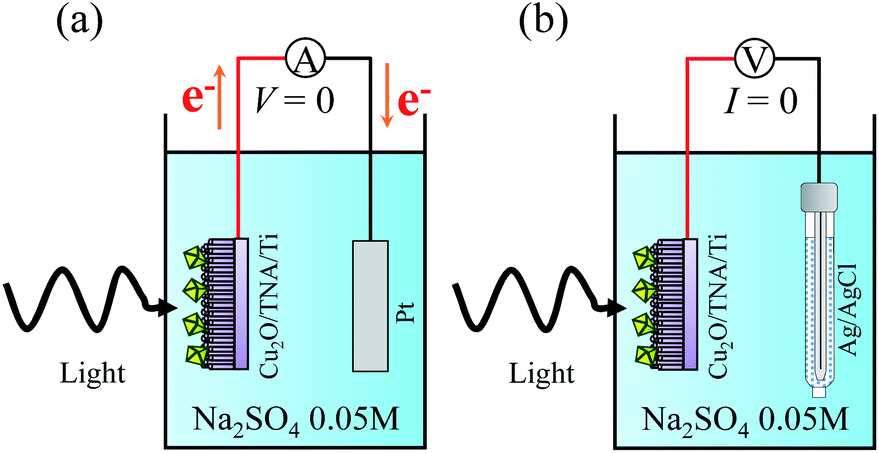 | ||
| Fig. 8 Schematics of the photocatalytic measurement under a two-electrode setup for (a) photocurrent intensity without bias and (b) OCP vs. Ag/AgCl. | ||
4. Conclusions
The photocatalytic properties of Cu2O/TNA/Ti, Cu2O/Ti, and Cu2O/FTO were studied. Without applied bias, Cu2O/TNA/Ti acted as a photoanode, whereas Cu2O/Ti and Cu2O/FTO acted as photocathodes. The Cu2O/TNA/Ti photoanode outperformed the other two Cu2O/Ti and Cu2O/FTO photocathodes in photocatalysis. Cu2O/TNA/Ti demonstrated the best photocatalytic activity to R6G, with a rate twice that of Cu2O/Ti and Cu2O/FTO over a period of 120 min. The photoanodic and photocathodic characteristics of Cu2O on different substrates can be described by their energy band diagrams. No charge separation enhancement at the Cu2O/TNA/Ti, Cu2O/Ti, and Cu2O/FTO junctions was observed. Cu2O/TNA/Ti demonstrated superior photocatalytic properties compared with TNA/Ti, which were mainly attributable to the UV-visible light absorption of Cu2O.Conflicts of interest
There are no conflicts to declare.Acknowledgements
The authors would like to thank the Ministry of Science and Technology of Taiwan for their support of this research under grants MOST 109-2112-M-029-001 and 109-2112-M-029-006.References
- B. Balamurugan and B. R. Mehta, Thin Solid Films, 2001, 396, 90–96 CrossRef CAS.
- A. Chen, H. Long, X. Li, Y. Li, G. Yang and P. Lu, Vacuum, 2009, 83, 927–930 CrossRef CAS.
- P. E. de Jongh, D. Vanmaekelbergh and J. Kelly, ChemComm, 1999, 1069–1070 RSC.
- J.-N. Nian, C.-C. Hu and H. Teng, Int. J. Hydrogen Energy, 2008, 33, 2897–2903 CrossRef CAS.
- J. Choi, J. T. Song, H. S. Jang, M.-J. Choi, D. M. Sim, S. Yim, H. Lim, Y. S. Jung and J. Oh, Electron. Mater. Lett., 2017, 13, 57–65 CrossRef CAS.
- L. Liu, W. Yang, W. Sun, Q. Li and J. K. Shang, ACS Appl. Mater. Interfaces, 2015, 7, 1465–1476 CrossRef CAS.
- L. Pan, J. H. Kim, M. T. Mayer, M.-K. Son, A. Ummadisingu, J. S. Lee, A. Hagfeldt, J. Luo and M. Grätzel, Nat. Catal., 2018, 1, 412–420 CrossRef CAS.
- N. D. Khiavi, R. Katal, S. K. Eshkalak, S. Masudy-Panah, S. Ramakrishna and H. Jiangyong, Nanomaterials, 2019, 9, 1011 CrossRef CAS.
- R. Xue, X. Fan, Y. Liu, P. Li, Q. Liu and F. Liu, Chem. Phys. Lett., 2019, 730, 45–53 CrossRef CAS.
- S. Shyamal, P. Hajra, H. Mandal, J. K. Singh, A. K. Satpati, S. Pande and C. Bhattacharya, ACS Appl. Mater. Interfaces, 2015, 7, 18344–18352 CrossRef CAS.
- W. Siripala, A. Ivanovskaya, T. F. Jaramillo, S.-H. Baeck and E. W. McFarland, Sol. Energy Mater. Sol. Cells, 2003, 77, 229–237 CrossRef CAS.
- W. Z. Tawfik, M. A. Hassan, M. A. Johar, S.-W. Ryu and J. K. Lee, J. Catal., 2019, 374, 276–283 CrossRef CAS.
- A. S. Elmezayyen, S. Guan, F. M. Reicha, I. M. El-Sherbiny, J. Zheng and C. Xu, J. Phys. D: Appl. Phys., 2015, 48, 175502 CrossRef.
- C. Wang, J. Xu, S. Shi, Y. Zhang, Z. Liu, X. Zhang, S. Yin and L. Li, RSC Adv., 2016, 6, 4422–4428 RSC.
- J. Zhang, H. Zhu, S. Zheng, F. Pan and T. Wang, ACS Appl. Mater. Interfaces, 2009, 1, 2111–2114 CrossRef CAS.
- Z. Bai and Y. Zhang, J. Alloys Compd., 2016, 675, 325–330 CrossRef CAS.
- J. Zhang, H. Ma and Z. Liu, Appl. Catal., B, 2017, 201, 84–91 CrossRef CAS.
- B. Peng, S. Zhang, S. Yang, H. Wang, H. Yu, S. Zhang and F. Peng, Mater. Res. Bull., 2014, 56, 19–24 CrossRef CAS.
- X. Xu, Z. Gao, Z. Cui, Y. Liang, Z. Li, S. Zhu, X. Yang and J. Ma, ACS Appl. Mater. Interfaces, 2016, 8, 91–101 CrossRef CAS.
- A. Amtout and R. Leonelli, Phys. Rev. B, 1995, 51, 6842–6851 CrossRef CAS.
- H. Tang, K. Prasad, R. Sanjinès, P. E. Schmid and F. Lévy, J. Appl. Phys., 1994, 75, 2042–2047 CrossRef CAS.
- M. Ni, M. K. H. Leung, D. Y. C. Leung and K. Sumathy, Renewable Sustainable Energy Rev., 2007, 11, 401–425 CrossRef CAS.
- H. Wender, A. F. Feil, L. B. Diaz, C. S. Ribeiro, G. J. Machado, P. Migowski, D. E. Weibel, J. Dupont and S. R. Teixeira, ACS Appl. Mater. Interfaces, 2011, 3, 1359–1365 CrossRef CAS.
- C. B. D. Marien, T. Cottineau, D. Robert and P. Drogui, Appl. Catal., B, 2016, 194, 1–6 CrossRef CAS.
- Y. Liao, P. Deng, X. Wang, D. Zhang, F. Li, Q. Yang, H. Zhang and Z. Zhong, Nanoscale Res. Lett., 2018, 13, 221 CrossRef.
- J. Wang, G. Ji, Y. Liu, M. A. Gondal and X. Chang, Catal. Commun., 2014, 46, 17–21 CrossRef CAS.
- K.-L. Chang, Q. Sun, Y.-P. Peng, S.-W. Lai, M. Sung, C.-Y. Huang, H.-W. Kuo, J. Sun and Y.-C. Lin, Chemosphere, 2016, 150, 605–614 CrossRef CAS.
- Q. Sun, Y.-P. Peng, H. Chen, K.-L. Chang, Y.-N. Qiu and S.-W. Lai, J. Hazard. Mater., 2016, 319, 121–129 CrossRef CAS.
- B. A. Koiki, B. O. Orimolade, B. N. Zwane, D. Nkosi, N. Mabuba and O. A. Arotiba, Electrochim. Acta, 2020, 340, 135944 CrossRef CAS.
- Y. L. Liu, Y. C. Liu, R. Mu, H. Yang, C. L. Shao, J. Y. Zhang, Y. M. Lu, D. Z. Shen and X. W. Fan, Semicond. Sci. Technol., 2004, 20, 44–49 CrossRef.
- C. Adán, J. Marugán, E. Sánchez, C. Pablos and R. van Grieken, Electrochim. Acta, 2016, 191, 521–529 CrossRef.
- L. Xiang, J. Ya, F. Hu, L. Li and Z. Liu, Appl. Phys. A, 2017, 123, 160 CrossRef.
- M. Chapman and W. B. Euler, J. Fluoresc., 2018, 28, 1431–1437 CrossRef CAS.
- M. E. Aguirre, R. Zhou, A. J. Eugene, M. I. Guzman and M. A. Grela, Appl. Catal., B, 2017, 217, 485–493 CrossRef CAS.
- M. G. Helander, M. T. Greiner, Z. B. Wang, W. M. Tang and Z. H. Lu, J. Vac. Sci. Technol., A, 2011, 29, 011019 CrossRef.
- F. Johnson, S. H. Song, J. Abrahamson, R. Liptak, E. Aydil and S. A. Campbell, Sol. Energy Mater. Sol. Cells, 2015, 132, 515–522 CrossRef CAS.
- S. L. Shinde and K. K. Nanda, RSC Adv., 2012, 2, 3647–3650 RSC.
- J. Li, Z. Mei, D. Ye, H. Liang, L. Liu, Y. Liu, A. Galeckas, A. Y. Kuznetsov and X. Du, Opt. Mater. Express, 2013, 3, 2072–2077 CrossRef.
- R. E. Rex, F. J. Knorr and J. L. McHale, J. Phys. Chem. C, 2013, 117, 7949–7951 CrossRef CAS.
- D. K. Pallotti, L. Passoni, P. Maddalena, F. Di Fonzo and S. Lettieri, J. Phys. Chem. C, 2017, 121, 9011–9021 CrossRef CAS.
Footnote |
| † Electronic supplementary information (ESI) available. See DOI: 10.1039/d0ra10681j |
| This journal is © The Royal Society of Chemistry 2021 |