
 Open Access Article
 This Open Access Article is licensed under a Creative Commons Attribution-Non Commercial 3.0 Unported Licence
Enhanced performance of ZnO nanorod array/CuSCN ultraviolet photodetectors with functionalized graphene layers
Guangcan Luo†
 a,
Ziling Zhang†a,
Jing Jianga,
Yang Liua,
Wei Li*a,
Jingquan Zhanga,
Xia Haob and
Wenwu Wanga
a,
Ziling Zhang†a,
Jing Jianga,
Yang Liua,
Wei Li*a,
Jingquan Zhanga,
Xia Haob and
Wenwu Wanga
aCollege of Materials Science and Engineering, Sichuan University, Chengdu 610064, China. E-mail: waylee2000@sohu.com; Tel: +86-28-85412542
bInstitute of New Energy and Low-carbon Technology, Sichuan University, Chengdu 610027, China
First published on 17th February 2021
Abstract
Facile, convenient and low-cost processes, including a chemical hydrothermal method and impregnation technique, were demonstrated to fabricate a self-powered ZnO nanorod array/CuSCN/reduced graphene oxide (rGO) ultraviolet photodetector. ZnO nanorods (NRs) were fully filled and encased by the CuSCN layer, in which CuSCN acts as the primary hole-transport layer and an electron reflection layer, blocking the electron transfer towards the Au electrode and reducing the electron–hole pair recombination. After annealing, this encapsulated structure further reduces the surface state defects of ZnO NRs, which can isolate the electron exchange with oxygen in the air, dramatically reducing the rise and fall time; it also forms a p–n junction, providing a built-in electric field to improve the photoresponse without applying external power. The rGO layer was coated on the surface of CuSCN as the secondary hole-transport layer and then annealed, which could effectively block Au from entering CuSCN and contacting ZnO along cracks and holes during vapor deposition, avoiding the formation of leakage channels. Furthermore, due to the ultra-high carrier mobility and the increase in work function after Au doping, the functionalized graphene could reduce the valence band shift, which is beneficial to enhance hole transport. Meanwhile, rGO obstructs the undesired barrier formed by electrical potential-induced reaction of Au with thiocyanate anions. Finally, the ZnO NR/CuSCN/rGO ultraviolet photodetector exhibits a significant enhancement in device performance (responsivity: 18.65 mA W−1 at 375 nm under 65 mW cm−2 illumination, rectification ratio: 5690 at ±1 V), which is better that of than ZnO NR/CuSCN structure (10.88 mA W−1, 10.22 at ±1 V) and maintains the 100 ms response time.
1. Introduction
Wide-bandgap semiconductor materials are suitable candidates for ultraviolet photodetectors (UV PDs), including diamond, ZnS, SnO2, GaN, SiC, ZnO, and TiO2.1 UV PDs show wide applications in fire monitoring, biological analysis, environmental sensors, missile plume detection, space exploration, and UV irradiation detection.2 Because few p-type wide band semiconductors exist, most UV PDs are based on n-type semiconductors, of which ZnO, a non-toxic and abundant semiconductor, has a band gap of 3.37 eV at room temperature, a large excitation binding energy of 60 meV, and a carrier mobility of 200 cm2 V−1 s−1.3 Recently, research interest has focused on the utilization of one-dimensional (1D) ZnO nanostructures to fabricate advanced UV PDs via various processes. 1D nanostructures, including nanorods, nanowires, nanotubes and nanobelts, with various compositions and morphologies have been deposited by many methods. 1D ZnO PDs exhibit excellent sensitivity and conductivity as well as a fast response rate due to the quantum confinement effect, surface effect, nonlinear optical effect, and dielectric confinement effect.2,4 Compared with ZnO PDs based on traditional thin-film and bulk materials, 1D ZnO PDs usually have high surface-area-to-volume ratios (SVRs) and reduced dimensions of the effective conductive channel; this can confine the active area of charge carriers, shorten the transit time and prolong the photocarrier lifetime, leading to large responsivity and photoconductive gain in nanoscale photodetectors.5,6Furthermore, various device configurations, such as photoconductor,7 metal–semiconductor–metal (MSM),8 Schottky barrier9 and p–n (or p–i–n),10,11 have been adopted for preparing UV PDs, in which the p–n junction and Schottky barrier UV PDs can be operated without external power supply, i.e., self-powered.12,13 Due to high SVRs, trapping at surface states drastically affects the transport and photoconduction properties of NRs. In the dark, when ZnO NRs are exposed to air, O2(g) is adsorbed on the ZnO NRs surface and captures free electrons present in the n-type oxide semiconductor [O2(g) + e− → O2−(ad)], and a low-conductivity depletion layer is formed near the surface. Upon illumination, electron–hole pairs are photogenerated [hv → e− + h+] when the photon energy is above the band gap (Eg). Holes migrate to the surface along the potential slope produced by band bending and discharge the negatively charged adsorbed oxygen ions [h+ + O2−(ad) → O2(g)]. Consequently, oxygen is photodesorbed from the surface. The unpaired electrons are either collected at the anode or recombine with holes generated when oxygen molecules are reabsorbed and ionized at the surface. This hole-trapping mechanism through oxygen adsorption and desorption in ZnO NRs augments the high density of trap states usually found in NRs due to the dangling bonds at the surface and thus enhances the NW photoresponse.8,14,15 However, a high bias voltage must be applied in order to obtain a high responsivity, which results in a long response time. ZnO-based p–n photodiodes have the advantages of fast response times, no applied fields, and no oxygen dependency. Self-powered ZnO UV PDs have previously been reported, including homojunctions and heterojunctions.16–19 p-Type ZnO is necessary to fabricate a homogeneous p–n junction photodiode. However, owing to the low solubility of the chosen dopant, strong lattice relaxation and self-compensation effect, it remains a challenge to obtain stable p-type ZnO by incorporating acceptor defects effectively.1,20 Hence, a variety of p-type materials are used to prepare p–n heterojunctions of UV PDs with n-type ZnO, including inorganic semiconductors (CuI, CuSCN, CuAlO2, GaN, etc.). Among them, CuSCN is a p-type semiconductor with a wide band gap of 3.6 eV, exhibiting high transparency in the visible range.11,21 It is also a promising hole transport material (HTM) due to its reasonable hole conductivity (≥5 × 10⁻⁴ S cm−1),22 and it can be easily grown by electrodeposition, successive ionic layer adsorption and reaction techniques.22–24 Additionally, CuSCN can be deposited via solution processes (impregnation techniques or spin-coating methods). Steve Dunn et al. firstly utilized spin-coating methods to construct a ZnO-nanorod/CuSCN UV photodetector that obtained a responsivity of 7.5 mA W−1 (@0.1 mV) with 6 mW cm−2 irradiance at 355 nm and a rise time of ≈500 ns, while the decay time was ≈6.7 μs.12 Then, Jérôme Garnier et al. successfully used impregnation techniques to fabricate ZnO nanowire/CuSCN heterojunctions which achieved a maximum rectification ratio of 2644 at ±2 V and a responsivity of 20 mA W−1 (@370 nm, 100 mW cm−2) after annealing at 150 °C under air atmosphere (the response time was not given).11 The CuSCN layer can be used as a hole transport layer and an electron reflection layer, rapidly transferring the holes and blocking the electron transfer towards the Au electrode so as to reduce the electron–hole pair recombination.25,26 However, the CuSCN film has low hole mobility of 0.01 cm2 V−1 s−1 (ref. 27 and 28) and will readily form an undesired barrier due to the electrical potential-induced reaction of gold with the thiocyanate anions.29 In order to enhance the ability of carriers to transport the interface and eliminate the barrier, rGO prepared by a modified Hummers method was incorporated between CuSCN and Au in this work.
Graphene or chemically modified graphene (CMG) is a potential material for use in perovskite solar cells,30 CdTe solar cells,31 organic solar cells,32 photodetectors,33 lithium batteries34 and gas sensors35 because its carrier mobility is extraordinary high even at room temperature.36 rGO, a kind of functionalized graphene, has residual oxygenated groups, which provide the foundation for its modified graphene properties37 and also do not affect carrier transport.38 Li et al.39 and Yun et al.40 have utilized GO and rGO as hole transport layers, and they obtained efficient and stable perovskite solar cells. Their results show that oxygen containing groups do not affect hole injection or transport. This is because carriers (both holes and electrons) can be injected and transported via the isolated lateral sp2 clusters which are in contact with the electrodes in a sandwich metal/GO/metal structure. Furthermore, it has been found that cells with rGO manifested much longer lifetimes than cells with PEDOT:PSS.
In order to improve the compatibility of graphene with various solvents and materials, functionalization of graphene is required, such as the introduction of modified molecules or ions based on intermolecular interactions or ionic bonds.41–43 Gong and Giovannetti et al. have calculated that the conductivity type and work function of graphene can be adjusted by doping different kinds of metals by first principles.44,45 Among these metals, Au can shift the Fermi level of graphene from the Dirac point into the valence band, which forms the p-type layer and improves the work function from 4.6 eV to 5.1 eV. This is more suitable for collecting holes and reducing the valence band shifts for hole transfer.46,47
In our work, a layer of CuSCN uniformly encapsulating ZnO nanorods was prepared using the drop-coating impregnation technique; then, rGO was drop-coated to prepare ZnO NR/CuSCN/rGO (ZCR) heterojunctions. A series of characterizations has revealed that functionalized graphene can reduce interface defects and enhance carrier transport, thus significantly improving device performance.
2. Experimental details
2.1 Synthesis of ZnO nanorods
ZnO NRs were grown on FTO glass substrate (10 Ω per square) by hydrothermal methods. The detailed experimental process has been reported elsewhere.48 First, zinc acetate dihydrate (0.01 M) and diethanolamine (0.02 M) were dissolved in 50 ml isopropanol by sustained heating and stirring at 65 °C for 1 h to achieve a transparent precursor solution. Afterwards, a thin ZnO nanoparticle seed layer was deposited on FTO substrate by spin-coating at a speed of 2000 rpm for 20 s repeated three times; then, it was annealed for 1 h at 300 °C under air atmosphere. Subsequently, ZnO-seeded substrates were dipped face-down inside a hydrothermal reactor, containing an equimolar solution (0.05 M) of zinc nitrate hexahydrate and hexamethylenetetramine (HMTA). The temperature of the solution was maintained at 80 °C for 4 h. The as-grown nanorods were washed thoroughly with deionized (DI) water, followed by annealing at 300 °C in ambient atmosphere for 1 h to improve the crystallinity of the ZnO NRs.2.2 Fabrication of ZnO NR/CuSCN/rGO heterostructures
ZnO NR/CuSCN/rGO heterostructures were formed by depositing a CuSCN layer on the ZnO nanorod arrays using drop-coating impregnation techniques, and the process flow diagram of the bilayer is shown in Fig. 1.11,49 0.1 g of CuSCN powder was initially dissolved in 10 ml propyl-sulfide, which is above the solubility of 0.4 M, to obtain a CuSCN suspension. After 24 h of stirring and 12 h of settling, a clear and lucid yellowish solution was achieved. In order to investigate the coverage of CuSCN on ZnO nanorods, we titrated 15–35 droplets of CuSCN solution with a pipette on 2 cm × 2 cm ZnO NRs, as shown in Fig. 2. Obviously, the thickness of the film became thicker with increasing number of droplets. 15 and 20 droplets did not cover the nanorods well. It should be noted that the CuSCN thin films were too thick after titrating >30 droplets, after which the carrier mobility was very low for carrier transportation. Therefore, 25 droplets of as-prepared solution were deposited on the sample and maintained at 100 °C to favor solvent evaporation and preferentially fill the pores between the ZnO NRs, followed by annealing at 150 °C in air for 1 h to improve the interface properties between the ZnO NRs and CuSCN layer.11 After cooling to room temperature, the rGO film was prepared on the surface of CuSCN layer from a 1 mg ml−1 DMF solution by applying the dip-coating process and annealed at 100 °C for 60 min to form a hole-transport bilayer along with a CuSCN membrane. Finally, 80 nm Au films were deposited on the surface of the rGO layer by vacuum evaporation, and the photodetectors were scribed to 0.09 cm2 by laser pulse scribing equipment. For comparison, the device of the ZnO NR/CuSCN (ZC) structure was also prepared.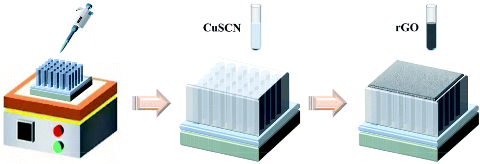 | ||
| Fig. 1 The process flow diagram of the CuSCN/rGO bilayer. | ||
 | ||
| Fig. 2 The cross-sectional SEM images of the CuSCN thickness with different droplets: (a) 15 droplets, (b) 20 droplets, (c) 25 droplets, (d) 30 droplets and (e) 35 droplets. | ||
2.3 Characterization
Scanning electron microscopy (Zeiss Sigma 300) was used to evaluate the surface morphologies of the samples, and energy-dispersive X-ray (EDAX Inc. SMART EDX) was applied to analyze the ratio of Cu and S atoms. The structures of the obtained films were measured from X-ray photoelectron diffraction (XRD, DX-2600, Dandong, China) using Cu Kα1 (λ = 1.540598 Å) radiation. The quality of the samples was determined by Raman spectroscopy (RM, LabRAM HR). Transmittance measurements (PerkinElmer Lambda 950 ultraviolet-visible spectrometer) were used to study the optical properties of the samples in the wavelength range from 250 to 800 nm. The work function was measured with a Thermo Fisher ESCALAB 250Xi. The excitation light source is He I (the energy is 21.22 eV) and the Fermi level position is calibrated by Au under the applied voltage of −5 V. Electrochemical impedance spectroscopy (EIS) was recorded using an electrochemical workstation (CHI660D, Chenhua, Shanghai) under dark conditions. The measured frequency ranged from 10−1 Hz to 106 Hz, and the amplitude was set at 5 mV. The spectra were fitted by ZsimDemo software. The external quantum efficiency (EQE) was measured by QEX10 (PV Measurements, Inc.) and calibrated by standard Si photodiodes under monochromatic light irradiation at a power intensity of 65 mW cm−2 with a wavelength range from 300 to 450 nm. The data of dark I–V, light I–V and time-response were collected through a Keithley 2400 digital source meter. A mask (5 × 5 cm2), leaving only a circular hole 2 mm in diameter (Φ2) in the middle, was used in the photoresponse tests of the photodetector at room temperature. Under illumination, the mask was fitted closely to the glass surface, where light was incident from the hole to the device.3. Results and discussion
Fig. 3 shows the SEM images of typical cross-sectional morphologies of ZnO NRs arrays, ZnO NR/CuSCN heterojunctions and the top-view of ZnO NR/CuSCN/rGO. The ZnO nanorods were grown nearly vertically to the FTO substrate, above 1.1 μm in length and about 100 nm in diameter, similar to a trap structure which can enhance absorption of ultraviolet light, as shown in Fig. 3a. The gap between the nanorods is favorable for the impregnation and coverage of CuSCN, so that the nanorods can be completely encapsulated by CuSCN, as illustrated in Fig. 3b. With the large surface-area-to-volume ratios of the nanorods, the formed p–n junctions can rapidly separate the photogenerated carriers. After annealing, a rough surface with many porosities and many cracks forms for the deposited CuSCN layer (Fig. 3c) due to the rapid re-evaporation of internal propyl-sulfide. Once the rGO layer is added, the surface roughness decreases and the cracks diminish remarkably (Fig. 3d). The reason could be that during titration of rGO dispersions, DMF solvent penetrates into the cracks of CuSCN to generate a re-dissolution process, and the subsequent low temperature annealing at 100 °C does not cause the formation of cracks due to slow evaporation of the solvent; thus, the majority of cracks are mostly eliminated. Energy dispersive X-ray (EDX) analysis (Fig. 4a) was utilized to evaluate the stoichiometry of the CuSCN layer. Because of the interference of residual carbon and nitrogen in the specimen chamber, only the ratio of Cu and S is used to determine the conductivity type. The atom ratio of [Cu]/[SCN] is less than 1, indicating that the CuSCN obtained by the impregnation technique is a p-type layer.11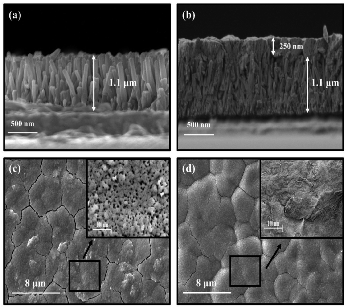 | ||
| Fig. 3 The cross-sectional SEM images of (a) ZnO NRs and (b) ZnO NR/CuSCN and top-views of (c) ZnO NR/CuSCN and (d) ZnO NR/CuSCN/rGO. | ||
 | ||
| Fig. 4 (a) EDX spectrum of ZnO NR/CuSCN and elemental atomic ratio of [Cu]/[S], (b) XRD patterns of the FTO, FTO based ZnO NRs, CuSCN and rGO, (c) Raman spectra of FTO, FTO based ZnO NRs, CuSCN and rGO, (d) UV-visible transmittance of FTO, FTO/ZnO NRs, FTO/ZnO NR/CuSCN and FTO/ZnO NR/CuSCN/rGO, (e) the variation of (ahv)2 versus the photon energy (hv) for ZnO NRs. | ||
The XRD patterns of the as-prepared samples on FTO substrate are shown in Fig. 4b. The intensity of the X-ray diffraction is logarithmic to distinguish the weak peaks from the other phases. ZnO nanorods prepared by the hydrothermal method show a very sharp diffraction peak at 34.42°, suggesting a highly preferential orientation of (001) with high crystallinity. The other weak peaks at 36.25°, 47.53° and 62.86° can be attributed to diffraction from the (101), (102), and (103) planes, respectively (JCPDS 36-1451). After subtracting the diffraction peak from the FTO substrate, all the diffraction peaks can be well indexed to the trigonal-phase β-CuSCN50 (JCPDS 29-0581) and hexagonal wurtzite structure of ZnO with a predominant (001) growth orientation, where no characteristic peaks from other phases of CuSCN or impurity phases can be observed, indicating high purity and crystallinity of the CuSCN deposited using the drop-coating impregnation technique. The characteristic peak of the coated rGO at 25° is not observed because of the peak of the FTO substrate. In addition, the rGO does not result in the phase transformation of CuSCN and/or the formation of intermediate products.
Fig. 4c shows the Raman spectra of all samples excited by 2.33 eV radiation in vacuum environments. Based on the reported zone-center optical phonon frequencies in ZnO,51 the peaks at 188, 393, 440, and 609 cm−1 can be assigned to the second order Raman spectrum arising from zone-boundary phonons 2-TA (M), A1 transverse-optic (TO) phonons, E2 modes and E1 longitudinal-optic (LO) phonons, respectively. These are typical phonons confined in the nanostructure (i.e., ZnO nanorods).52 From the figure, the Raman characteristic peaks of CuSCN are all β-phase.53 The intense line can be assigned to Cu–N and Cu–S vibration modes at 201 and 246 cm−1, δ (SCN) bending modes at 431 and 875 cm−1, and the bridging thiocyanate group region v (SCN) (stretching v (C–N) mode) at 2176 cm−1, respectively.11 No shifting of the Raman peaks of CuSCN or other hetero peaks can be seen after the addition of rGO; this indicates that rGO has not changed its properties, showing only a faint lift of the D and G peaks.54
As shown in Fig. 4d, the FTO substrate has an excellent transmittance in the UV-A band, and the light before 390 nm is completely absorbed by 1.1 μm ZnO NRs (3.37 eV). This is because the vertical structure (FTO/ZnO NR/CuSCN/rGO/Au, where light enters from the backside of FTO substrate) is used in this experiment, and the UV light is completely absorbed by the ZnO NRs before reaching CuSCN (3.6 eV).22 Therefore, the p-type CuSCN does not generate carriers, but serves as a hole transport layer, forming a built-in electric field with n-type ZnO NRs to become self-powered photodetectors. After adding a layer of rGO, the response range to the UV band is not changed, and the effect on the visible light transmittance is also minimal. The ZnO nanorods act as the active layer in the device, and the band gap (Eg) conculcated by the Tauc formula is 3.24 eV (Fig. 4e), which is lower than pure ZnO (3.37 eV) at room temperature, and the reason is that the defect density increases with the increasing specific surface area, leading to the formation of defect levels in the band gap of ZnO.55
In order to fabricate high-performance, low-cost and self-powered photodetectors and avoid the electrical potential-induced reaction of gold with the thiocyanate anions,29 rGO was then drop-coated on the CuSCN layer. The adsorption energy of the molecular adsorbates on the CuSCN surfaces is dependent on the film orientation. This is attributed to the large number of dangling bonds available in the CuSCN surface, which leads to stronger interactions between the CuSCN (001) surface and the molecules.56 Therefore, the oxygen-containing groups of rGO readily adsorb and homogeneously cover the CuSCN (001) surface, both inhibiting the reaction between Au and SCN− and allowing carrier transport via the isolated lateral sp2 clusters. However, the intrinsic work function of graphene is 4.6 eV,46 which does not align favorably with the band energy of CuSCN and Au. Fortunately, some studies show that the work function and conductivity type of graphene will change after metal doping.44,57 After graphene contacts metal atoms, its work function will change (i.e., functionalized graphene).58,59 The results from theoretical calculations by G. Giovannetti et al. show that when graphene is adsorbed on Au film, the unique energy band structure of graphene does not change; however, this interaction leads to charge transfer, so that the Fermi level of graphene can be shifted down by up to 0.5 eV with respect to the Dirac point, which was also verified by the experimental results of M. M. Giangregori et al. In order to calculate the work function of rGO after contacting the Au film in this experiment, a 5 nm Au film was deposited on a clean Si/SiO2 (300 nm) substrate (Fig. 5a); then, the rGO film was prepared on the Si/SiO2(300 nm)/Au substrate (Fig. 5b and d). As a comparison, the work function of rGO was also tested on Si/SiO2(300 nm) substrate (Fig. 5c). The work function Φ of rGO using UPS measurements can be calculated based on the Einstein equation:60
| Φ = hν − (Ecutoff − EF) | (1) |
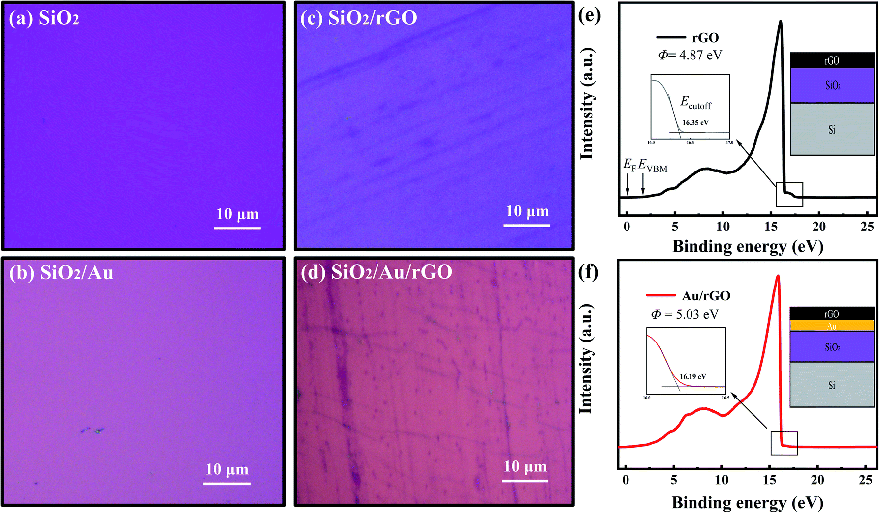 | ||
| Fig. 5 Optical images of (a) Si/SiO2 substrate, (b) Si/SiO2/Au substrate, (c) Si/SiO2/rGO, and (d) Si/SiO2/Au/rGO, and the UPS spectrum of (e) rGO and (f) Au/rGO. | ||
A schematic of a UV photodetector with the ZnO NR/CuSCN/rGO heterojunction on FTO-coated glass substrate is shown in Fig. 6a. The surface and interstices of the ZnO NRs are completely encapsulated and filled with CuSCN, and the nanorods exhibit an embedded structure in the thin film. Fig. 6b shows the energy band diagram of the device. The bandgap of ZnO is about 3.37 eV, and the position of the conduction band is 4.2 eV under vacuum.17 The bandgap of CuSCN is about 3.6 eV, and the position of the conduction band is 1.5 eV;22 therefore, the electron–hole pairs are mainly photogenerated in the ZnO NRs through the absorption of UV-A incident photons.11 Under UV irradiation, the electron–hole pairs generated from the ZnO NRs are separated by the p–n junction formed with CuSCN; then, the electrons are reflected by CuSCN and collected by FTO, and the holes are collected by rGO/Au, respectively. Simultaneously, due to the different work functions of ZnO NRs (4.33 eV),61 CuSCN (5 eV)11 and rGO/Au (5.1 eV)46,62 and the large junction area, the electron–hole pairs are rapidly separated to inhibit carrier recombination and achieve a self-powered device.
 | ||
| Fig. 6 (a) Schematic and (b) energy band of the FTO/Zn NR/CuSCN/rGO/Au junction. | ||
J–V measurements of the ZC and ZCR heterojunctions are shown in Fig. 7a. The two types of diodes exhibit significant rectifier behavior. Due to the favorable interfacial contact formed by CuSCN filling and wrapping between the ZnO nanorods and lack of reverse junctions, the ZC and ZCR devices have no roll-over phenomenon, even at high bias voltage (>1 V). Furthermore, owing to the blocking of the formation of leakage channels and elimination of undesired barriers by rGO, the performance of the ZCR device is improved, with enhanced diode behavior, reduced leakage current and a high rectification ratio (∼5690 at ±1 V). Meanwhile, the reverse saturation current density (J0) and diode ideality factor (η) can be calculated by the Shockley equation:63
 | (2) |
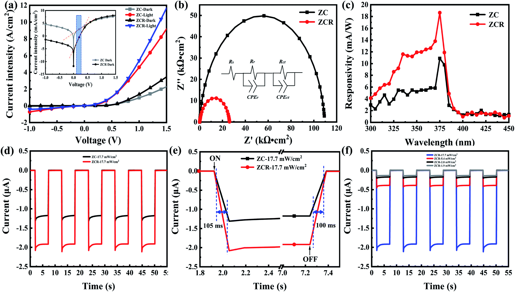 | ||
| Fig. 7 (a) Dark and 365 nm light I–V curves, (b) EIS spectra of the ZC and ZCR junctions, (c) wavelength-dependent responsivity spectra of ZC and ZCR under 65 mW cm−2 with 0 V, (d) time-dependent photoresponse of ZC and ZCR at 365 nm under the illumination of 17.7 mW cm−2, (e) the rise and fall times of the ZC and ZCR photodetectors at −1 μV, (f) photocurrent measured at −1 μV bias under UV irradiances of 1.9, 2.8, 5.4 and 17.7 mW cm−2. | ||
Fig. 7b shows the Nyquist plots of the ZCR and ZC devices and the corresponding equivalent circuit. Note that Rr is the recombination resistance at the p–n junction at the low-frequency arc, Rct is a parallel resistor representing the level of difficulty of the charge transfer process at the high-frequency arc, and for the constant phase element (CPE), the non-ideal frequency-dependent capacitor, it is generally assumed that the non-ideal behavior originates from a distribution in the current density due to the material inhomogeneity. Rr and CPEr are related to the ZnO NR/CuSCN main junction, and Rct and CPEct are connected with the two electrical contacts between FTO/ZnO and CuSCN/Au.27,65 By the analysis of ZsimDemo software, the Rr increases from 2.5 × 10⁴ Ω (ZC) to 2.8 × 10⁵ Ω (ZCR). The high Rr can be beneficial for carrier separation and demonstrates fewer cracks between the ZnO NRs and CuSCN interface. Moreover, the Rct decreases from 1.2 × 10⁶ Ω (ZC) to 1 × 10⁴ Ω (ZCR), illustrating that rGO facilitates carrier transport and reduces interface recombination.
The wavelength-dependent responsivity spectra are shown in Fig. 7c. The responsivity was calculated from the external quantum efficiency (EQE):1,2,48
 | (3) |
 represent the ability of photodetectors to detect weak light signals. The NEP is given by33
 | (4) |
 can be obtained from33,48
 | (5) |
 can be written as67,68
 | (6) |
Therefore, from Fig. 7a and c, the detectivity at 375 nm under 65 mW cm−2 increases from 2.2 × 10¹⁰ (for ZC) to 3.7 × 1011 cm Hz1/2 W−1 (for ZCR). Additionally, the responsivity of the two devices is close to 1 mA W−1 at wavelengths above 400 nm, indicating that they are highly transparent to the visible band. With the secondary hole transport layer rGO, the highest UV (375 nm) to visible (450 nm) rejection ratio increases from 8.24 to 16.95 for ZnO nanorod-based detectors, thereby enhancing the anti-noise capability of the device.
Fig. 7d shows the stability and the response speed of the ZC and ZCR devices at a small reverse bias of ≈−1 μV under UV irradiance (365 nm) of 17.7 mW cm−2 switched on and off for five repeat cycles. The photocurrent was observed to be consistent and repeatable. The ZCR device has a significantly higher responsive current than the ZC device. The signal-to-noise ratio (i.e., SNR = (Iλ − Id)/Id, where Iλ is the photocurrent under 365 nm light illumination and Id is the dark current given above)69 also increases from 2.2 × 10³ (ZC) to 3.6 × 10³ (ZCR), which is consistent with the calculation of the detectivity. Moreover, the response time is another important indicator for photodetector performance, including the rise time τr and the fall time τf,70 as shown in Fig. 7e. Coincidentally, the rise and fall times of the ZC and ZCR devices are nearly identical, about 105 ms (τr) and 100 ms (τf), respectively. In other words, in addition to enhancing the responsivity, rGO can maintain the fast response time of the device.9,71 Meanwhile, the photosensitivities of the ZnO/CuSCN/rGO device under 365 nm UV irradiance of 1.9–17.7 mW cm−2 were tested (Fig. 7f), which shows that the photocurrent response increases with the irradiation intensity and that the photodetector is remarkably stable and repeatable. Table 1 compares the performance of self-powered ZnO NR/CuSCN/rGO photodetectors with previous research of similarly constructed devices based on ZnO nanomaterials. Our ZCR photodetectors, fabricated by facile, convenient and low-cost processes, exhibit excellent rectification ratio properties and millisecond response times.
| Structure | Wavelength/intensity | Rectification ratio | Responsivity (bias voltage) | Rise time/fall time | Detectivity (Jones) | Ref. |
|---|---|---|---|---|---|---|
| ZnO NRs | 365 nm/0.1 mW cm−2 | — | 0.445 A W−1 (2 V) | — | 6.27 × 10¹¹ | 55 |
| CuSCN | 280 nm/0.22 mW cm−2 | — | 79 A W−1 (2 V) | 1–50 s | — | 72 |
| GQD–ZnO nanorods/PEDOT:PSS | 340 nm/80 mW cm−2 | — | 36 A W−1 (−1 V) | — | 1.3 × 10¹² | 48 |
| RGO/ZnO nanowires | UV/3.26 mW cm−2 | — | 16.46 A W−1 (1 V) | 28.46 s/9.76 s | 1.14 × 10¹⁴ | 18 |
| Graphene/ZnO NR array | 365 nm/100 μW cm−2 | — | 113 A W−1 (−1 V) | 0.7 ms/3.6 ms | — | 71 |
| GQDs/ZnO-NRs/GaN-NTs | 325 nm/3.2 mW cm−2 | 3.2 × 10⁶ (−6 V) | 159 ms/68.7 ms | 7.0 × 10¹¹ | 14 | |
| ZnO–CuI/CuSCN | 370 nm/5.5 mW cm−2 | 103 (±1 V) | 13 mA W−1 (0 V) | < 0.1 s | — | 27 |
| ZnO-nanorod/CuSCN | 355 nm/6 mW cm−2 | — | 7.5 mA W−1 (0.1 mV) | 500 ns/6.7 μs | — | 12 |
| 9.5 A W−1 (−5 V) | ||||||
| ZnO nanowire/CuSCN | 370 nm/100 mW cm−2 | 2644 (±2 V) | 20 mA W−1 (0 V) | — | — | 11 |
| ZnO NR/CuSCN/rGO | 375 nm/65 mW cm−2 | 5690 (±1 V) | 18.65 mA W−1 (−1 μV) | 105 ms/100 ms | 3.7 × 10¹¹ | This work |
4. Conclusions
The CuSCN/rGO hole-transport bilayers were applied in nanorod ZnO-based heterojunctions by using a simple, convenient, and low-cost drop coating method to obtain enhanced performance of self-powered photodetectors with high responsivity, fast response, and excellent repeatability and stability. The CuSCN completely fills and encapsulates the ZnO nanorods to form a stable p–n junction, and it acts as the primary hole-transport layer and an electron reflection layer to effectively separate carriers and reduce carrier recombination. On the other hand, rGO as the secondary hole-transport layer significantly reduces the cracks of CuSCN and effectively inhibits the reaction between gold and SCN−. With the increase of the work function of rGO by Au doping, the barrier of carrier transport is decreased. As a result, the rectification ratio of 5690 (at ±1 V) and a responsivity of 18.65 mA W−1 were obtained at 375 nm under 65 mW cm−2 illumination.Conflicts of interest
The authors declare that there is no conflict of interests regarding the publication of this paper.Acknowledgements
This work was supported by National Natural Science Foundation of China (No. 61704115), and Science and Technology Program of Sichuan Province, China (Grant No. 2020YFSY0064, 2019YFG0262, 2019ZDZX0015).References
- F. Teng, K. Hu, W. Ouyang and X. Fang, Adv. Mater., 2018, 30, 1706262 CrossRef.
- W. Tian, H. Lu and L. Li, Nano Res., 2015, 8, 382–405 CrossRef CAS.
- H. Chen, H. Liu, Z. Zhang, K. Hu and X. Fang, Adv. Mater., 2016, 28, 403–433 CrossRef CAS.
- H. Chen, K. Liu, L. Hu, A. A. Al-Ghamdi and X. Fang, Mater. Today, 2015, 18, 493–502 CrossRef CAS.
- L. Peng, L. Hu and X. Fang, Adv. Mater., 2013, 25, 5321–5328 CrossRef CAS.
- G. Shen and D. Chen, Recent Pat. Nanotechnol., 2010, 4, 20–31 CrossRef CAS.
- Y. Takahashi, M. Kanamori, A. Kondoh, H. Minoura and Y. Ohya, Jpn. J. Appl. Phys., 1994, 33, 6611–6615 CrossRef CAS.
- C. Soci, A. Zhang, B. Xiang, S. A. Dayeh, D. P. Aplin, J. Park, X. Y. Bao, Y. H. Lo and D. Wang, Nano Lett., 2007, 7, 1003–1009 CrossRef CAS.
- L. Duan, F. He, Y. Tian, B. Sun, J. Fan, X. Yu, L. Ni, Y. Zhang, Y. Chen and W. Zhang, ACS Appl. Mater. Interfaces, 2017, 9, 8161–8168 CrossRef CAS.
- Z. Bai, J. Liu, F. Liu and Y. Zhang, J. Alloys Compd., 2017, 726, 803–809 CrossRef CAS.
- J. Garnier, R. Parize, E. Appert, O. Chaix-Pluchery, A. Kaminski-Cachopo and V. Consonni, ACS Appl. Mater. Interfaces, 2015, 7, 5820–5829 CrossRef CAS.
- S. M. Hatch, J. Briscoe and S. Dunn, Adv. Mater., 2013, 25, 867–871 CrossRef CAS.
- H. D. Cho, A. S. Zakirov, S. U. Yuldashev, C. W. Ahn, Y. K. Yeo and T. W. Kang, Nanotechnology, 2012, 23, 115401 CrossRef.
- L. Goswami, N. Aggarwal, R. Verma, S. Bishnoi, S. Husale, R. Pandey and G. Gupta, ACS Appl. Mater. Interfaces, 2020, 12, 47038–47047 CrossRef CAS.
- L. Goswami, N. Aggarwal, M. Singh, R. Verma, P. Vashishtha, S. K. Jain, J. Tawale, R. Pandey and G. Gupta, ACS Appl. Nano Mater., 2020, 3, 8104–8116 CrossRef CAS.
- W. Dai, X. Pan, S. Chen, C. Chen, W. Chen, H. Zhang and Z. Ye, RSC Adv., 2015, 5, 6311–6314 RSC.
- K. B. Ko, B. D. Ryu, M. Han, C.-H. Hong, D. A. Dinh and T. V. Cuong, Appl. Surf. Sci., 2019, 481, 524–530 CrossRef CAS.
- C. Chen, S. Zhang, B. Hu, H. San, Z. Cheng and W. Hofmann, Composites, Part B, 2019, 164, 640–647 CrossRef CAS.
- F. Cao and X. Ji, J. Mater. Sci.: Mater. Electron., 2018, 29, 6594–6600 CrossRef CAS.
- Y. W. Heo, S. J. Park, K. Ip, S. J. Pearton and D. P. Norton, Appl. Phys. Lett., 2003, 83, 1128–1130 CrossRef CAS.
- C. Xiong, R. H. Yao, W. J. Wan and J. X. Xu, Optik, 2014, 125, 785–788 CrossRef CAS.
- Q. Zhang, H. Guo, Z. Feng, L. Lin, J. Zhou and Z. Lin, Electrochim. Acta, 2010, 55, 4889–4894 CrossRef CAS.
- C. Liu, W. Wu, K. Liu, M. Li, G. Hu and H. J. C. Xu, CrystEngComm, 2012, 14, 6750–6754 RSC.
- B. R. Sankapal, E. Goncalves, A. Ennaoui and M. C. Luxsteiner, Thin Solid Films, 2004, 451, 128–132 CrossRef.
- V. E. Madhavan, I. Zimmermann, A. A. B. Baloch, A. Manekkathodi, A. Belaidi, N. Tabet and M. K. Nazeeruddin, ACS Appl. Energy Mater., 2019, 3, 114–121 CrossRef.
- A. Montgomery, L. Guo, C. Grice, R. A. Awni, S. Saurav, L. Li, Y. Yan and F. Yan, Prog. Photovoltaics, 2019, 665–672 CAS.
- Z. Yang, M. Wang, J. Ding, Z. Sun, L. Li, J. Huang, J. Liu and J. Shao, ACS Appl. Mater. Interfaces, 2015, 7, 21235–21244 CrossRef CAS.
- P. Pattanasattayavong, G. O. Ndjawa, K. Zhao, K. W. Chou, N. Yaacobi-Gross, B. C. O'Regan, A. Amassian and T. D. Anthopoulos, Chem. Commun., 2013, 49, 4154–4156 RSC.
- N. Arora, M. I. Dar, A. Hinderhofer, N. Pellet, F. Schreiber, S. M. Zakeeruddin and M. Gratzel, Science, 2017, 358, 768–771 CrossRef CAS.
- C. Redondo-Obispo, T. S. Ripolles, S. Cortijo-Campos, A. L. Álvarez, E. Climent-Pascual, A. de Andrés and C. Coya, Mater. Des., 2020, 191, 108587 CrossRef CAS.
- X. Bi, G. C. Luo, W. Li, J. Q. Zhang, L. L. Wu, B. Li, G. G. Zeng and W. W. Wang, Sol. Energy, 2018, 170, 820–827 CrossRef CAS.
- Y. Dang, Y. Wang, S. Shen, S. Huang, X. Qu, Y. Pang, S. R. P. Silva, B. Kang and G. Lu, Org. Electron., 2019, 67, 95–100 CrossRef CAS.
- X. Li, T. Sun, K. Zhou, X. Hong, X. Tang, D. Wei, W. Feng, J. Shen and D. Wei, Nanotechnology, 2020, 31, 315204 CrossRef CAS.
- F. Khan, M. Oh and J. H. Kim, Chem. Eng. J., 2019, 369, 1024–1033 CrossRef CAS.
- G. Murali, M. Reddeppa, C. Seshendra Reddy, S. Park, T. Chandrakalavathi, M. D. Kim and I. In, ACS Appl. Mater. Interfaces, 2020, 12, 13428–13436 CrossRef CAS.
- X. Du, I. Skachko, A. Barker and E. Y. Andrei, Nat. Nanotechnol., 2008, 3, 491–495 CrossRef CAS.
- W. S. Hummer and R. E. Offeman, J. Am. Chem. Soc., 1958, 80, 1339 CrossRef.
- Y. Hu, S. Song and A. Lopez-Valdivieso, J. Colloid Interface Sci., 2015, 450, 68–73 CrossRef CAS.
- S. S. Li, K. H. Tu, C. C. Lin, C. W. Chen and M. Chhowalla, ACS Nano, 2010, 4, 3169–3174 CrossRef CAS.
- J. M. Yun, J. S. Yeo, J. Kim, H. G. Jeong, D. Y. Kim, Y. J. Noh, S. S. Kim, B. C. Ku and S. I. Na, Adv. Mater., 2011, 23, 4923–4928 CrossRef CAS.
- Z. Zhang, P. Lin, Q. Liao, Z. Kang, H. Si and Y. Zhang, Adv. Mater., 2019, 31, 1806411 CrossRef.
- H. C. Schniepp, J. L. Li, M. J. McAllister, H. Sai, M. Herrera-Alonso, D. H. Adamson, R. K. Prud'homme, R. Car, D. A. Saville and I. A. Aksay, J. Phys. Chem. B, 2006, 110, 8535–8539 CrossRef CAS.
- A. K. Mishra and S. Ramaprabhu, J. Phys. Chem. C, 2011, 115, 14006–14013 CrossRef CAS.
- G. Giovannetti, P. A. Khomyakov, G. Brocks, V. M. Karpan, J. van den Brink and P. J. Kelly, Phys. Rev. Lett., 2008, 101, 026803 CrossRef CAS.
- C. Gong, G. Lee, B. Shan, E. M. Vogel, R. M. Wallace and K. Cho, J. Appl. Phys., 2010, 108, 123711 CrossRef.
- Y. Shi, K. K. Kim, A. Reina, M. Hofmann, L. J. Li and J. Kong, ACS Nano, 2010, 4, 2689–2694 CrossRef CAS.
- C. Gong, D. Hinojos, W. Wang, N. Nijem, B. Shan, R. M. Wallace, K. Cho and Y. J. Chabal, ACS Nano, 2012, 6, 5381–5387 CrossRef CAS.
- S. Dhar, T. Majumder and S. P. Mondal, ACS Appl. Mater. Interfaces, 2016, 8, 31822–31831 CrossRef CAS.
- G. R. R. A. Kumara, A. Konno, G. K. R. Senadeera, P. V. V. Jayaweera, D. B. R. A. De Silva and K. Tennakone, Sol. Energy Mater. Sol. Cells, 2001, 69, 195–199 CrossRef CAS.
- B. Marí, K. C. Singh, L. Ortiz and M. Mollar, J. Solid State Electrochem., 2012, 17, 667–673 CrossRef.
- M. Rajalakshmi, A. K. Arora, B. S. Bendre and S. Mahamuni, J. Appl. Phys., 2000, 87, 2445–2448 CrossRef CAS.
- R. Zhang, P.-G. Yin, N. Wang and L. Guo, Solid State Sci., 2009, 11, 865–869 CrossRef CAS.
- Y. Son, N. R. de Tacconi and K. Rajeshwar, J. Electroanal. Chem., 1993, 345, 135–146 CrossRef CAS.
- C. Chen, T. Chen, H. Wang, G. Sun and X. Yang, Nanotechnology, 2011, 22, 405602 CrossRef.
- H. Zheng, Y. Jiang, S. Yang, Y. Zhang, X. Yan, J. Hu, Y. Shi and B. Zou, J. Alloys Compd., 2020, 812, 152158 CrossRef CAS.
- L. Zhang and Y. Chen, J. Phys. Chem. C, 2019, 123, 26785–26793 CrossRef CAS.
- P. A. Khomyakov, G. Giovannetti, P. C. Rusu, G. Brocks, J. van den Brink and P. J. Kelly, Phys. Rev. B: Condens. Matter Mater. Phys., 2009, 79, 195425 CrossRef.
- Y. K. Kim, H. Jang and K. Kang, Bull. Korean Chem. Soc., 2017, 38, 1042–1046 CrossRef CAS.
- B. S. He and G. A. Du, Anal. Methods, 2017, 9, 4341–4348 RSC.
- Y. Park, V. Choong, Y. Gao, B. R. Hsieh and C. W. Tang, Appl. Phys. Lett., 1996, 68, 2699–2701 CrossRef CAS.
- Y. Tang, J. Chen, D. Greiner, L. Aé, R. Baier, J. Lehmann, S. Sadewasser and M. C. Lux-Steiner, J. Phys. Chem. C, 2011, 115, 5239–5243 CrossRef CAS.
- M. M. Giangregorio, W. Jiao, G. V. Bianco, P. Capezzuto, A. S. Brown, G. Bruno and M. Losurdo, Nanoscale, 2015, 7, 12868–12877 RSC.
- R. A. Awni, D.-B. Li, C. R. Grice, Z. Song, M. A. Razooqi, A. B. Phillips, S. S. Bista, P. J. Roland, F. K. Alfadhili, R. J. Ellingson, M. J. Heben, J. V. Li and Y. Yan, Sol. RRL, 2019, 3, 1800304 CrossRef.
- S. Das Sarma, S. Adam, E. H. Hwang and E. Rossi, Rev. Mod. Phys., 2011, 83, 407–470 CrossRef CAS.
- Y. Y. Proskuryakov, K. Durose, M. K. Al Turkestani, I. Mora-Seró, G. Garcia-Belmonte, F. Fabregat-Santiago, J. Bisquert, V. Barrioz, D. Lamb, S. J. C. Irvine and E. W. Jones, J. Appl. Phys., 2009, 106, 044507 CrossRef.
- R. M. Geisthardt and J. R. Sites, IEEE Journal of Photovoltaics, 2014, 4, 1114–1118 Search PubMed.
- S. Dhar, T. Majumder and S. P. Mondal, Mater. Res. Bull., 2017, 95, 198–203 CrossRef CAS.
- Y. Liu, Y. Zhang, K. Zhao, Z. Yang, J. Feng, X. Zhang, K. Wang, L. Meng, H. Ye, M. Liu and S. F. Liu, Adv. Mater., 2018, 1707314 CrossRef.
- S. Li, D. Guo, P. Li, X. Wang, Y. Wang, Z. Yan, Z. Liu, Y. Zhi, Y. Huang, Z. Wu and W. Tang, ACS Appl. Mater. Interfaces, 2019, 11, 35105–35114 CrossRef CAS.
- H. Lin, L. Wei, C. Wu, Y. Chen, S. Yan, L. Mei and J. Jiao, Nanoscale Res. Lett., 2016, 11, 420 CrossRef.
- B. Nie, J. G. Hu, L. B. Luo, C. Xie, L. H. Zeng, P. Lv, F. Z. Li, J. S. Jie, M. Feng, C. Y. Wu, Y. Q. Yu and S. H. Yu, Small, 2013, 9, 2872–2879 CrossRef CAS.
- G. Wyatt-Moon, D. G. Georgiadou, J. Semple and T. D. Anthopoulos, ACS Appl. Mater. Interfaces, 2017, 9, 41965–41972 CrossRef CAS.
Footnote |
| † These authors contributed equally to this work. |
| This journal is © The Royal Society of Chemistry 2021 |