
 Open Access Article
 This Open Access Article is licensed under a Creative Commons Attribution-Non Commercial 3.0 Unported Licence
Electron-assisted synthesis of g-C3N4/MoS2 composite with dual defects for enhanced visible-light-driven photocatalysis
Jingxuan Zheng†
,
Bo Zhang† and
Zhao Wang *
*
National Engineering Research Centre of Industry Crystallization Technology, School of Chemical Engineering and Technology, Tianjin University, Tianjin 300072, China. E-mail: wangzhao@tju.edu.cn
First published on 22nd December 2020
Abstract
g-C3N4/MoS2 composites were successfully prepared by an electron-assisted strategy in one step. Dielectric barrier discharge (DBD) plasma as an electron source, which has low bulk temperature and high electron energy, can etch and modify the surface of g-C3N4/MoS2. The abundant N and S vacancies were introduced in the composites by plasma. The dual defects promoted the recombination and formation of heterojunctions of the g-C3N4/MoS2 composite. It exhibited stronger light harvesting ability and higher charge separation efficiency than that of pure g-C3N4 and MoS2. Compared with the sample by traditional calcination method, the plasma-sample showed better performance for degrading rhodamine B (RhB) and methyl orange. RhB is completely degraded within 2 hours on g-C3N4/MoS2 by plasma. A mechanism for the photocatalytic degradation of organic pollutants via the composites was proposed. An electron-assisted strategy provides a green and effective platform to achieve catalysts with improved performance.
Introduction
Due to the rapid development of industrialization, environmental pollution especially water pollution is becoming more and more serious. Various practical strategies have been developed for efficient removal of organic pollutants from wastewater.1 The photocatalytic process shows great potential as a green, low cost and sustainable treatment technology in the wastewater industry.2 Semiconductor mediated photocatalysis is a most used strategy, that has attracted great interest for the degradation of organic pollutants under solar radiation.g-C3N4, as a visible light-responsive semiconductor material, is characterized by low cost, convenient preparation, unique structure, non-toxicity, and harmlessness.3 MoS2, a layered material with a narrow band gap, is often used as a cocatalyst in various applications.4 Meanwhile, heterostructure materials have received extensive attention due to their unique physicochemical properties.5 Among them, the combination of g-C3N4 and MoS2 in heterostructured photocatalysts could effectively improve the photocatalytic degradation of organic pollutants. Fan et al. prepared a 2D g-C3N4/MoS2 composite by calcination and revealed that the composite shows good degradation activity for rhodamine B (RhB) and methyl orange (MO) under visible light.6 Chen et al. prepared a g-C3N4/MoS2 composite by vacuum freeze drying and demonstrated that this composite has good hydrogen production efficiency and pollutant degradation activity under visible light.7
Defect engineering can effectively improve the photochemical and electrocatalysis performance of semiconductor materials.8 A suitable concentration of defects can effectively reduce the recombination rate of electrons and holes, change the band gap structure, and enhance the light absorption capacity.9 Surface defects may also serve as physical adsorption or chemically active sites to improve photocatalytic reactions.10 Defect engineering can usually be achieved by chemical reduction method,11 high-temperature hydrogen reduction,12 and light reduction.13 Li et al. obtained WO3 with oxygen vacancies that could be used for water oxidation reactions by hydrogen roasting at 500 °C.12 Ye et al. prepared porous g-C3N4 by using 300 W Xe lamp heating combined with hydrazine reduction and applied the same to achieve hydrogen energy.13 Unfortunately, these synthesis methods usually feature long processing times, high energy consumption, and complicated processes. Therefore, applying the green, convenient, and fast method of new technology for catalyst preparation is an effective strategy.14
Among them, nonthermal plasma, which has a relatively low bulk temperature and extremely high electron temperature, has excellent advantages for preparing catalysts.15 Plasma can etch the surface of many materials and produce an abundance of defects. Defects of different concentrations can be prepared under different atmospheres and treatment times. For example, Wang et al. prepared Co3O4 with oxygen vacancies by using Ar plasma, the Co3O4 showed enhanced electrocatalytic oxygen evolution reaction performance.16 Feng et al. used dielectric barrier discharge (DBD) plasma to prepare TiO2 with oxygen vacancies and better performance for the photocatalytic degradation of pollutants.17
In this paper, N and S vacancies enriched g-C3N4/MoS2 composite was prepared using DBD plasma. X-ray diffraction (XRD), X-ray photoelectron spectroscopy (XPS), electron paramagnetic resonance (EPR), high-resolution transmission electron microscopy (HRTEM), and other characterization methods were used to analyze the physical and chemical properties of the composites. The vacancies and heterostructure of the composite ensure charge separation efficiency and strong light absorptive capacity. The photocatalytic performance of the composite was also tested by degrading RhB and MO under visible light. The strategy of producing defects by plasma can be applied to other nanosheet materials to enhance their photocatalytic performance.
Experimental
Materials
Melamine, ammonium tetrathiomolybdate, anhydrous ethanol, rhodamine B, triethanolamine were purchased from Shanghai Aladdin Biochemical Technology Co. All chemicals were used without further purification.Synthesis of g-C3N4
The pure g-C3N4 powder was synthesized by heating melamine powder directly. Typically, 10 g melamine was putted into a closed alumina crucible, then heated at 550 °C for 4 h with the rate of 5 °C min−1 in the muffle furnace. The as-prepared yellow product was grounded for further use.Synthesis of g-C3N4/MoS2
The schematic illustration for the preparation of g-C3N4/MoS2 composites can be seen from Scheme 1. First, 200 mg g-C3N4 powder was added to anhydrous ethanol under vigorous stirring, then (NH4)2MoS4 was added to the suspension and stirred for 12 hours. Then the mixture was dried in an oven at 353 K overnight for 2 h to remove the residual ethanol in the sample. The sample was then split into two portions. One portion was to be treated by calcination (and the other portion by plasma). For traditional calcination, the sample was calcined 500 °C at a rate of 5 °C min−1 in air for 2 hours. The sample prepared this way was designated as MCX-C. X represents the weight ratio of MoS2 in the composites. | ||
| Scheme 1 Schematic of the preparation of g-C3N4/MoS2 composites. | ||
The other portion was treated by DBD plasma. The details of treatment using plasma have been described in the previous work.30,31 The sample (about 0.2 g) was loaded on a quartz reactor that was placed between two electrodes. It was generated by applying 100 V and 2.0 A with H2–Ar (H2/Ar = 1/9 vol) as the plasma-forming gas. One-time plasma operation proceeded for 3 min to restrict the heat effect (IR camera shows the operation temperature is below 145 °C), followed by manually stirring to expose the untreated sample outside. The operation was repeated for 20 times, until total plasma treatment time was 1 h. The obtained samples were named MCX-D.
The pure g-C3N4 and (NH4)2MoS4 were also treated by plasma, and named g-C3N4-D and MoS2-D, respectively. (NH4)2MoS4 was calcined 500 °C at a rate of 5 °C min−1 in air for 2 hours and named MoS2-C.
Characterization
Rigaku D/Max-2500 V/PC diffractometer with Cu Kα1 radiation (Cu Kα1 α = 0.154 nm, 40 kV, 40 mA, 8 °min−1) was used to analyze the crystal phase of samples. Fourier transform infrared (FTIR) spectra was analyzed by Bruker Alpha FTIR-ATR instrument. A PHI-5000 VersaProbe instrument was used to obtain X-ray photoelectron spectra (XPS). The adventitious carbon C 1s used for element correction is located at 284.8 eV. Electron spin resonance (ESR) measurement was obtained on a Bruker A300 spectrometer at room temperature. The UV-vis diffuse-reflectance spectroscopy was recorded by a UV-2600 spectrophotometer. Photoluminescence (PL) spectroscopy was analyzed on F-4600 spectrometer with excitation at 350 nm. Scanning electron microscopy (SEM) and energy dispersive X-ray spectroscopy were conducted on S4800 instrument. High-resolution transmission electron microscopy (TEM) and energy dispersive X-ray elemental mapping were conducted on FEI Tecnai G20.Measurement of photocatalytic activity
Results and discussion
Fig. 1a shows the XRD spectra of the g-C3N4 and g-C3N4/MoS2 composites. Peaks corresponding to the (100) and (002) crystal planes of pure g-C3N4 appeared at 13.2° and 27.5°, which are attributed to the structure of tri-s-triazine and conjugated aromatic system, respectively.18 The peak of MoS2 was not observed in the XRD spectrum of the g-C3N4/MoS2 composite due to the low concentration of MoS2. In addition, the peak strength of the composite was weaker than that of pure g-C3N4. It indicates that g-C3N4 was successfully etched by plasma and its crystal structure had been changed. | ||
| Fig. 1 (a) XRD and (b) FTIR patterns of g-C3N4 and g-C3N4/MoS2 composites. | ||
Fourier transform infrared (FTIR) analysis was performed to analyze the composition and chemical bond information of the samples. Fig. 1b shows the FTIR spectra of pure g-C3N4 and the g-C3N4/MoS2 composite. The peak at 807 cm−1 in the spectrum of pure g-C3N4 is attributed to the tri-s-triazine unit structure. The four strong bands in the region of 1240–1640 cm−1 are attributed to the extension of the CN heterocyclic ring in g-C3N4.19 Vibrations between 3000 and 3500 cm−1 are caused by N–H and –OH tensile vibrations.20 No other changes were found in the composite. The FTIR results are consistent with the results observed by XRD.
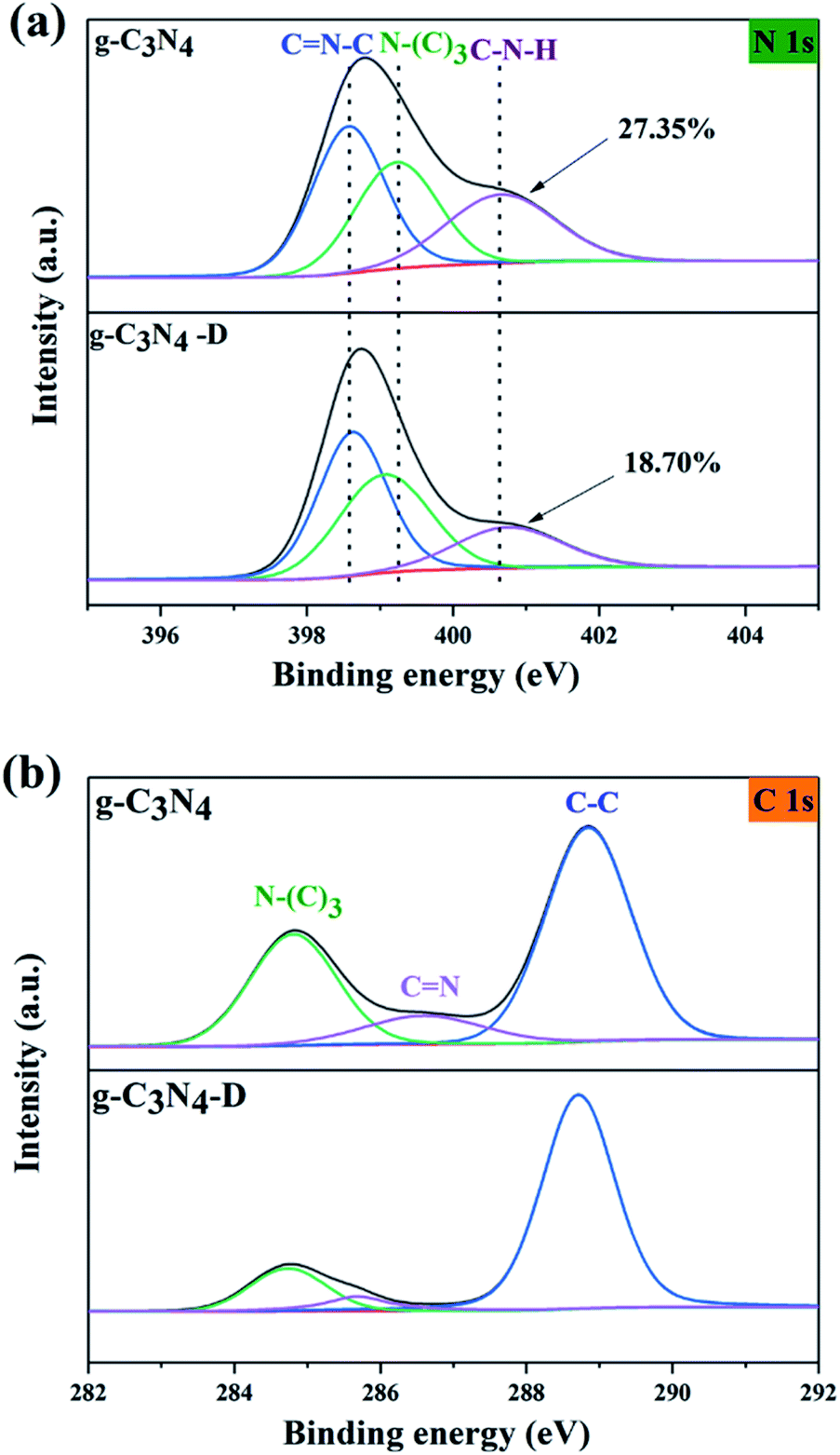
The XPS spectra of g-C3N4 by plasma treatment are shown in Fig. 2. Fig. 2a shows the high-resolution XPS spectrum of N 1s. The three characteristic peaks at 398.5, 399.2, and 400.6 eV were attributed to the action of C![[double bond, length as m-dash]](https://www.rsc.org/images/entities/char_e001.gif) N–C, N–(C)3, and C–N–H bonds, respectively.21 The escape of N atoms in the amino group on the surface of g-C3N4 is much easier to accomplish than other N atoms; therefore, the number of amino functional groups is consistent with the number of nitrogen defects.22 The proportions of the C–N–H peak areas g-C3N4 was untreated and treated with plasma were 27.35% and 18.70%, respectively. It indicates that N vacancies were generated on the surface of g-C3N4 by electron bombardment.
N–C, N–(C)3, and C–N–H bonds, respectively.21 The escape of N atoms in the amino group on the surface of g-C3N4 is much easier to accomplish than other N atoms; therefore, the number of amino functional groups is consistent with the number of nitrogen defects.22 The proportions of the C–N–H peak areas g-C3N4 was untreated and treated with plasma were 27.35% and 18.70%, respectively. It indicates that N vacancies were generated on the surface of g-C3N4 by electron bombardment.
 | ||
| Fig. 2 High-resolution XPS spectra of the (a) N 1s and (b) C 1s of g-C3N4. | ||
Fig. 2b shows the high-resolution XPS spectrum of C 1s. The peaks at 284.8, 255.6, and 288.4 eV are attributed to N–(C)3, CN, and C–C respectively.23 The peak area representing the CN bond decreased after plasma treatment. This result also indicates the successful generation of N vacancies. In summary, the chemical structure of g-C3N4 did not change by plasma, but N vacancies were produced on the surface of g-C3N4 under plasma etching.
The statistics of C/N atomic ratio were showed the absence of N atoms. Table 1 shows the changes of the C/N atomic ratio of g-C3N4 and MC0.01 before and after plasma treatment. The C/N atomic ratio of g-C3N4 after plasma treatment was changed from 0.921 to 0.954, which indicates the absence of N atoms. MC0.01-D also exhibited a C/N atomic ratio of 0.969, which is smaller than the C/N atomic ratio of the MC0.01-C (0.976). It indicates that plasma is efficient method for producing defects. The C/N atom ratio of the composites was slightly larger than that of pure g-C3N4 because of the MoS2 and g-C3N4 are closely combined.
| Samples | Atomic ratio (C![[thin space (1/6-em)]](https://www.rsc.org/images/entities/char_2009.gif) :N) :N) |
Peak area ratio: SC–N–H/Stotal |
|---|---|---|
| g-C3N4 | 0.921 | 0.273 |
| g-C3N4-D | 0.954 | 0.187 |
| MC0.01-C | 0.969 | 0.225 |
| MC0.01-D | 0.976 | 0.202 |
The XPS spectra of MC0.01-C and MC0.01-D are shown in Fig. 3. Fig. 3a and b show the high-resolution XPS spectra of C 1s and N 1s, respectively. The main characteristic peaks are similar to those of g-C3N4. Interestingly, the differences of the peak areas between the CN and C–N–H groups of the composite were not as large as those of pure g-C3N4 after plasma treatment. It is because MoS2 occupies the surface of g-C3N4 in the composite. As shown in Fig. 3c, the two characteristic peaks at 229.2 and 232.5 eV correspond to Mo 3d5/2 and Mo 3d3/2, respectively, which indicates that Mo is as Mo4+.24 The peak at 226.6 eV corresponds to S 2s. Fig. 3d shows the characteristic peaks of S 2p3/2 and S 2p1/2, which are located at 162 and 163.5 eV, respectively.25 (NH4)2MoS4 was successfully reduced to MoS2 by the plasma and successfully loaded on g-C3N4.
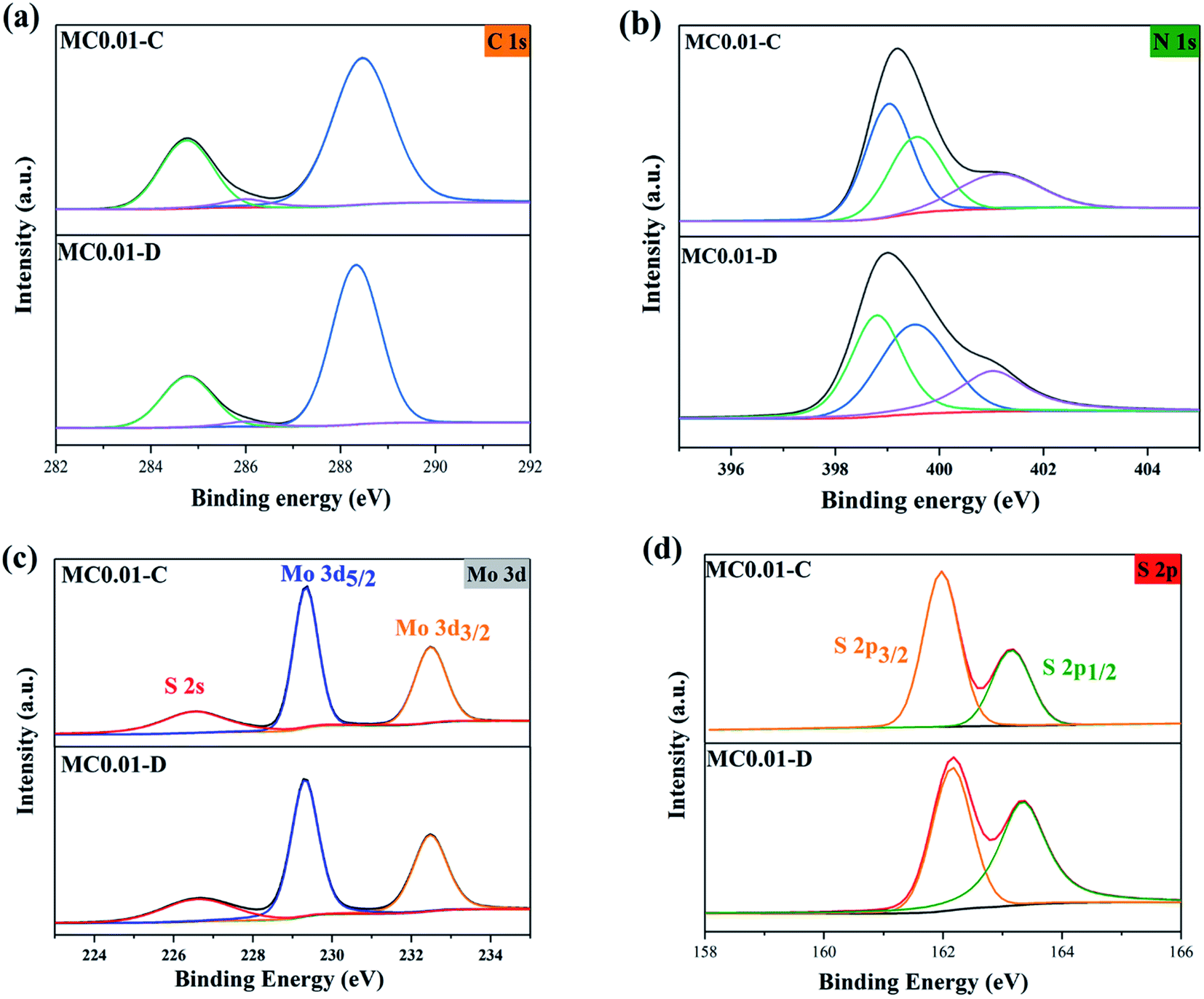 | ||
| Fig. 3 High-resolution XPS spectra of the (a) C 1s, (b) N 1s, (c) Mo 3d, and (d) S 2p of MC0.01-C and MC0.01-D. | ||
The defects of g-C3N4 and MoS2 were explored by EPR to investigate g-C3N4 and MoS2 samples by plasma treatment. As shown in Fig. 4a, g-C3N4 shows a signal peak at g = 2.003, which can be attributed to unpaired electrons on the sp2− carbon atoms of the aromatic rings within π bonds.26 Extra electrons remaining after the escape of N atoms could affect delocalized carbon atoms between π bonds and result in the formation of more asymmetric electrons.26 The peak intensity increased after plasma treatment; thus, more N vacancies were generated by plasma treatment. According to Fig. 4b, both plasma treated and untreated MoS2 samples have characteristic peaks of ∼3500 G, and the MoS2 prepared by plasma has weaker peak intensity than that prepared by calcination. This characteristic peak can be attributed to the presence of dangling Mo–S bonds. A higher peak intensity indicates a lower concentration of S vacancies.27 Therefore, MoS2-D has more S vacancies than that of MoS2-C. The sample obtained by plasma treatment has a high concentration of S vacancies, which plays a key role in improving its photocatalytic performance. The existence of N and S vacancies also provides strong interaction for the combination of g-C3N4 and MoS2.
 | ||
| Fig. 4 EPR spectra of (a) g-C3N4 and (b) MoS2. | ||
The results of XRD, XPS and EPR strongly proved that the N and S defects on the g-C3N4/MoS2 surface were successfully introduced with the assistance of plasma. The defect generation mechanism could be explained as: during the plasma discharge, Ar and H2 were ionized into Ar* and H*, and produced a lot of high-energy electrons. During the process, S in the MoS2 lattice was bombarded by Ar* and e−, causing it to escape from the lattice and leaving S vacancies.28 The N in the C3N4 lattice escaped by e− bombardment and was captured by H* to form ammonia, forming a stable N vacancy on the crystal surface,29 thereby reducing the coordination number of C in the two coordination environments of C–N–H and CN–C. More importantly, the defect introduction strategy assisted by electrons could efficiently construct defect sites without damaging the crystal structure, which proved that plasma is a gentle and efficient way to construct vacancies.
The morphological characteristics of MC0.01 composites were analyzed by scanning electron microscopy (SEM). As shown in Fig. 5a, the sample show the layered structure, which is typical of g-C3N4. Fig. 5b shows that the surface of the plasma-treated sample is rougher than that of calcinated sample because of electron impact. It confirms the plasma etching is the main reason to the production of defects.
 | ||
| Fig. 5 SEM images of (a) MC0.01-C and (b) MC0.01-D. (c–f) HRTEM images of MC0.01-D. | ||
A high-resolution TEM image of MC0.01-D is shown in Fig. 5c–f. As shown in Fig. 5c and 6d, g-C3N4 has a large sheet-like structure with several stacked layers, while MoS2 shows smaller nanosheets loaded on g-C3N4. It indicates that MoS2 nanosheets were successfully loaded onto g-C3N4 by plasma treatment that formed a heterogeneous interface. The strong interaction can facilitate charge transfer and improve the efficiency of charge analysis. As shown in Fig. 5e, MoS2 lattice fringes appeared at the edge of g-C3N4; thus, MoS2 was loaded on the surface layer of g-C3N4. Fig. 5f presents a high-resolution image of these lattice fringes. The width of the lattice is 0.625 nm, which corresponds to the (002) crystal plane of MoS2.
 | ||
| Fig. 6 STEM-EDX elemental mapping of MC0.01-D. | ||
Scanning transmission electron microscopy with energy-dispersive X-ray spectroscopy (STEM-EDX) elemental mapping analysis was performed to explore the distribution of the composite elements. Fig. 6 shows that the C and N elements are densely and uniformly distributed, whereas the S and Mo elements are distributed on the edge positions. It is consistent with the results of HRTEM.
The UV-visible diffuse reflection spectrum (UV-vis DRS) of the samples IS shown in Fig. 7a. The graph converted by the Kubelka–Munk algorithm function is shown in Fig. 7b to reveal the band gap of the material more accurately. The visible light absorption edge of pure g-C3N4 is located at 460 nm, and its corresponding band gap width is 2.70 eV.30 The visible light absorption range of the composites gradually expanded as increasing of MoS2. MC0.03-D exhibited a maximum absorption edge of 483 nm and a corresponding band gap width of 2.65 eV. Light response intensity also increased in the range of 450–800 nm with increasing of MoS2. The band gaps of MC0.01-D and MC0.01-C were 2.67 and 2.69 eV, respectively. Thus, plasma-sample has better light absorption ability than calcination-sample due to more N and S vacancies. The vacancies change the electronic structure and promote the light absorption ability of the as-prepared materials8a,17
 | ||
| Fig. 7 (a) UV-vis DRS and (b) the relationship between (ahv)2 and hv of g-C3N4 and g-C3N4/MoS2 composites. (c) PL spectra and (d) photocurrent density curve of MC0.01-D and MC0.01-C. | ||
Photoluminescence (PL) spectroscopy was performed to investigate the charge recombination of the samples. The PL peak intensity is negatively correlated with the electron–hole separation efficiency of a material.3a As shown in Fig. 7c, MC0.01-D has a lower peak intensity, which means it has a higher electron–hole separation efficiency,31 compared with MC0.01-C. The large number of vacancies increases the donor energy level of the material and promotes the efficiency of charge separation.32 The photocurrent density curve in Fig. 7d shows that MC0.01-D can produce a higher current density than MC0.01-C under the same light conditions; current density directly affects the extent of photocatalytic reaction. In summary, the vacancies improve the light absorption ability and the charge separation efficiency of the material, thereby enhancing its photocatalytic performance.
Organic pollutants were degraded under visible light to evaluate the photocatalytic activity of the prepared samples. Fig. 8a shows the photocatalytic degradation of RhB by g-C3N4 and g-C3N4/MoS2 under visible light irradiation. The pure g-C3N4 showed the lowest photocatalytic activity, and its degradation rate reached 64% within 2 h. The photocatalytic activity of the composites improved with increasing MoS2 loading because the interface between MoS2 and g-C3N4 promote charge transport. The photocatalytic degradation activity of the composite was highest when its MoS2 loading was 1%. Degradation on MC0.01-D was completed within 2 h. The activity of the composites decreased when the MoS2 loading was further increased because of a decrease of active sites on surface of g-C3N4. It shows that an appropriate loading amount is necessary to achieve optimal activity.33 The degradation efficiency of MC0.01-C was 79% within 2 h, which is much lower than that of MC0.01-D. MC0.01-D has an abundance of N and S vacancies that promote light absorption and charge separation.
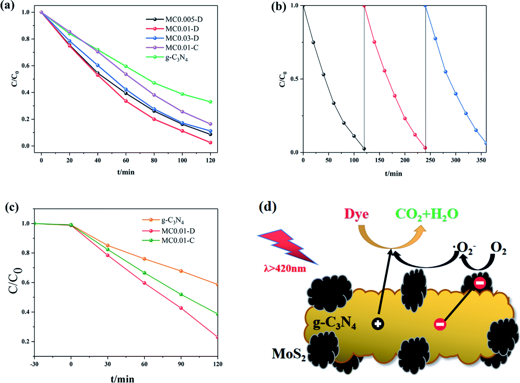 | ||
| Fig. 8 (a) Photocatalytic degradation of RhB by g-C3N4 and g-C3N4/MoS2 samples under visible light irradiation. (b) Photodegradation stability of RhB over MC0.01-D. (c) Photocatalytic degradation of MO by g-C3N4 and MC0.01 under visible light irradiation. (d) Mechanism of the photocatalytic degradation of dyes by g-C3N4/MoS2 composites. | ||
The stability of the samples was also investigated in photodegradation of RhB. As shown in Fig. 8b, the degradation rate of the samples decreased slightly after three cycles of degradation. It indicates that the composites prepared by plasma have strong stability. The prepared samples were also applied to the photocatalytic degradation of MO. As shown in Fig. 8c, MC0.01-D has higher activity than MC0.01-C. It also confirms the previous results.
The mechanism of the photocatalytic degradation of dyes on g-C3N4/MoS2 composites is shown in Fig. 8d. Electrons and holes were generated on g-C3N4 when exposed to light. The conduction band of g-C3N4 is more negative compared with the conduction band of MoS2; hence, electrons can be transferred from the conduction band of the former to that of the latter.6 These electrons react with surface adsorbed oxygen to generate superoxide radicals.34 ·O2− plays a key role in degrading dye. Holes in g-C3N4 are directly transported to the surface of the samples to react with the dye. At the same time, the existence of N vacancies caused the distance between adjacent C atoms to be significantly shortened, forming new C–C bonds, thereby significantly changing the surface electronic structure.35 And after the formation of N defects, the Fermi level moves to the bottom of the conduction band, which makes the material exhibit metallic properties and significantly reduces the band gap.35 Furthermore, the introduction of S vacancies would cause MoS2 to exhibit a transition from an indirect to a direct band gap, thereby further reducing the charge transfer resistance.36 Finally, organic dyes are degraded into CO2 and H2O. So, the N and S defects on g-C3N4/MoS2 composites, which facilitates the recombination and formation of heterojunction. It helps light absorption and charge transfer in photocatalytic degradation.
Conclusions
g-C3N4/MoS2 composites were prepared via an environment-friendly and efficient electron assisted plasma technology. The heterogeneous interface between g-C3N4 and MoS2 promotes charge transfer and improves photocatalytic performance of the composite. Plasma etching produces an abundance of N and S vacancies on the surface of g-C3N4/MoS2. These vacancies increased the light absorption capacity of the composite and improved their charge separation efficiency. The photocatalytic degradation efficiency of the composite by plasma was highest when the MoS2 was loaded 1 wt%, and the composite completely degrade organic pollutants within 2 h. Plasma technology has unique advantages in produce defects and preparation of heterostructured composites with prospective application as photocatalysts for pollutant degradation.Author contributions
Jingxuan Zheng: conceptualization, data curation, formal analysis. Bo Zhang: investigation, writing – original draft. Zhao Wang: supervision, writing – review & editing.Conflicts of interest
There are no conflicts to declare.Acknowledgements
This work was supported by National Key Research and Development Program of China (No. 2016YFF0102503), National Natural Science Foundation of China (No. 21878214) and State Key Laboratory of Efficient Utilization for Low Grade Phosphate Rock and Its Associated Resources (no. WFKF2019-03) are greatly appreciated.References
- (a) J. Y. Wang, T. P. Zhang, M. Li, Y. Yang, P. Lu, P. Ning and Q. Wang, RSC Adv., 2018, 8, 22694–22709 RSC; (b) W.-J. Ong, L.-L. Tan, Y. H. Ng, S.-T. Yong and S.-P. Chai, Chem. Rev., 2016, 116, 7159–7329 CrossRef CAS; (c) H. Agbe, E. Nyankson, N. Raza, D. Dodoo-Arhin, A. Chauhan, G. Osei, V. Kumar and K.-H. Kim, J. Ind. Eng. Chem., 2019, 72, 31–49 CrossRef CAS; (d) W. Zhong, S. Shen, S. Feng, Z. Lin, Z. Wang and B. Fang, CrystEngComm, 2018, 20, 7851–7856 RSC.
- (a) X. Guan, Y. Ren, S. Chen, J. Yan, G. Wang, H. Zhao, W. Zhao, Z. Zhang, Z. Deng and Y. Zhang, J. Mater. Sci., 2020, 55, 5808–5822 CrossRef CAS; (b) R. Katal, S. Masudy-Panah, M. Tanhaei, M. H. D. A. Farahani and H. Jiangyong, Chem. Eng. J., 2020, 384, 123384 CrossRef CAS; (c) Z. Wang, C. Li and K. Domen, Chem. Soc. Rev., 2019, 48, 2109–2125 RSC.
- (a) M. B. Tahir, M. Sagir and K. Shahzad, J. Hazard. Mater., 2019, 363, 205–213 CrossRef CAS; (b) V. Hasija, P. Raizada, A. Sudhaik, K. Sharma, A. Kumar, P. Singh, S. B. Jonnalagadda and V. K. Thakur, Appl. Mater. Today, 2019, 15, 494–524 CrossRef; (c) L. L. Liu, X. Y. Song, X. X. Kong, Q. Duan and E. W. Zhu, RSC Adv., 2020, 10, 9116–9125 RSC.
- (a) S. Y. Park, Y. H. Kim, S. Y. Lee, W. Sohn, J. E. Lee, Y.-S. Shim, K. C. Kwon, K. S. Choi, H. J. Yoo and J. M. Suh, J. Mater. Chem. A, 2018, 6, 5016–5024 RSC; (b) J. Y. O. Choi, M. C. O. Kim, S. Y. Moon, H. Kim, Y. S. Kim and K. W. Park, RSC Adv., 2020, 10, 19077–19082 RSC; (c) S. Chandrasekaran, L. Yao, L. Deng, C. Bowen, Y. Zhang, S. Chen, Z. Lin, F. Peng and P. Zhang, Chem. Soc. Rev., 2019, 48, 4178–4280 RSC.
- (a) D. Li, J. Zhang, S. M. Ahmed, G. Suo, W. A. Wang, L. Feng, X. Hou, Y. Yang, X. Ye and L. Zhang, J. Colloid Interface Sci., 2020, 574, 174–181 CrossRef CAS; (b) G. Suo, D. Li, L. Feng, X. Hou, X. Ye, L. Zhang, Q. Yu, Y. Yang and W. Wang, J. Mater. Chem. A, 2020, 55, 167–172 Search PubMed; (c) G. Suo, J. Zhang, D. Li, Q. Yu, M. He, L. Feng, X. Hou, Y. Yang, X. Ye, L. Zhang and W. A. Wang, J. Colloid Interface Sci., 2020, 566, 427–433 CrossRef CAS; (d) W. Zhong, S. Shen, M. He, D. Wang, Z. Wang, Z. Lin, W. Tu and J. Yu, Appl. Catal., B, 2019, 258 CrossRef.
- J. Li, E. Liu, Y. Ma, X. Hu, J. Wan, L. Sun and J. Fan, Appl. Surf. Sci., 2016, 364, 694–702 CrossRef CAS.
- J. Tian, Z. Chen, J. Jing, C. Feng, M. Sun and W. Li, J. Photochem. Photobiol., A, 2020, 390, 112260 CrossRef CAS.
- (a) S. Bai, N. Zhang, C. Gao and Y. Xiong, Nano Energy, 2018, 53, 296–336 CrossRef CAS; (b) W. Zhong, Z. Wang, N. Gao, L. Huang, Z. Lin, Y. Liu, F. Meng, J. Deng, S. Jin, Q. Zhang and L. Gu, Angew. Chem., Int. Ed., 2020, 59, 22743–22748 CrossRef CAS.
- (a) J. Xiong, J. Di, J. Xia, W. Zhu and H. Li, Adv. Funct. Mater., 2018, 28, 1801983 CrossRef; (b) X. Jiao, Z. Chen, X. Li, Y. Sun, S. Gao, W. Yan, C. Wang, Q. Zhang, Y. Lin, Y. Luo and Y. Xie, J. Am. Chem. Soc., 2017, 139, 7586–7594 CrossRef CAS; (c) H. Pan, J. Mater. Sci., 2015, 50, 4324–4329 CrossRef CAS.
- N. Zhang, C. Gao and Y. Xiong, J. Energy Chem., 2019, 37, 43–57 CrossRef.
- Y.-C. Zhang, Z. Li, L. Zhang, L. Pan, X. Zhang, L. Wang, A. Fazale and J.-J. Zou, Appl. Catal., B, 2018, 224, 101–108 CrossRef CAS.
- Y. Wang, J. Cai, M. Wu, J. Chen, W. Zhao, Y. Tian, T. Ding, J. Zhang, Z. Jiang and X. Li, Appl. Catal., B, 2018, 239, 398–407 CrossRef CAS.
- L. Shi, L. Yang, W. Zhou, Y. Liu, L. Yin, X. Hai, H. Song and J. Ye, Small, 2018, 14, 1703142 CrossRef.
- Z. Wang, B. Xiao, Z. Lin, S. Shen, A. Xu, Z. Du, Y. Chen and W. Zhong, J. Energy Chem., 2021, 54, 510–518 CrossRef.
- (a) Z. Wang, Y. Zhang, E. C. Neyts, X. Cao, X. Zhang, B. W. L. Jang and C.-j. Liu, ACS Catal., 2018, 8, 2093–2110 CrossRef CAS; (b) X. M. Tao, C. Sun, L. Huang, Y. Y. Han and D. Y. Xu, RSC Adv., 2019, 9, 6379–6386 RSC; (c) X. Peng, Z. Wang, Z. Wang and Y. Pan, Front. Chem. Sci. Eng., 2018, 12, 790–797 CrossRef CAS.
- L. Xu, Q. Jiang, Z. Xiao, X. Li, J. Huo, S. Wang and L. Dai, Angew. Chem., Int. Ed., 2016, 55, 5277–5281 CrossRef CAS.
- Y. Li, W. Wang, F. Wang, L. Di, S. Yang, S. Zhu, Y. Yao, C. Ma, B. Dai and F. Yu, Nanomaterials, 2019, 9, 720 CrossRef CAS.
- (a) B. Zhang, Z. Wang, X. Peng, Z. Wang, L. Zhou and Q. Yin, Nanomaterials, 2019, 9, 1139 CrossRef CAS; (b) X. Peng, Z. Wang, Z. Wang, J. Gong and H. Hao, Catal. Today, 2019, 337, 63–68 CrossRef CAS.
- H. Xie, Y. Zhao, H. Li, Y. Xu and X. Chen, J. Mater. Sci., 2019, 54, 10836–10845 CrossRef CAS.
- Y. Liu, X. Guo, Z. Chen, W. Zhang, Y. Wang, Y. Zheng, X. Tang, M. Zhang, Z. Peng, R. Li and Y. Huang, Appl. Catal., B, 2020, 266, 118624 CrossRef.
- (a) C. Zhou, D. Huang, P. Xu, G. Zeng, J. Huang, T. Shi, C. Lai, C. Zhang, M. Cheng, Y. Lu, A. Duan, W. Xiong and M. Zhou, Chem. Eng. J., 2019, 370, 1077–1086 CrossRef CAS; (b) Q. Liu, J. Shen, X. Yu, X. Yang, W. Liu, J. Yang, H. Tang, H. Xu, H. Li, Y. Li and J. Xu, Appl. Catal., B, 2019, 248, 84–94 CrossRef CAS.
- (a) P. Niu, L.-C. Yin, Y.-Q. Yang, G. Liu and H.-M. Cheng, Adv. Mater., 2014, 26, 8046–8052 CrossRef CAS; (b) Y. Kang, Y. Yang, L.-C. Yin, X. Kang, L. Wang, G. Liu and H.-M. Cheng, Adv. Mater., 2016, 28, 6471 CrossRef CAS.
- W.-J. Ong, L.-L. Tan, S.-P. Chai and S.-T. Yong, Dalton Trans., 2015, 44, 1249–1257 RSC.
- (a) Y. Jiao, Q. Huang, J. Wang, Z. He and Z. Li, Appl. Catal., B, 2019, 247, 124–132 CrossRef CAS; (b) L. Tian, R. Wu and H. Liu, J. Mater. Sci., 2019, 54, 9656–9665 CrossRef CAS.
- Y.-J. Yuan, Z. Shen, S. Wu, Y. Su, L. Pei, Z. Ji, M. Ding, W. Bai, Y. Chen, Z.-T. Yu and Z. Zou, Appl. Catal., B, 2019, 246, 120–128 CrossRef CAS.
- L. Yang, J. Huang, L. Shi, L. Cao, Q. Yu, Y. Jie, J. Fei, H. Ouyang and J. Ye, Appl. Catal., B, 2017, 204, 335–345 CrossRef CAS.
- (a) B. Sun, Z. Liang, Y. Qian, X. Xu, Y. Han and J. Tian, ACS Appl. Mater. Interfaces, 2020, 12, 7257–7269 CrossRef CAS; (b) Y. Liu, Y. Xie, L. Liu and J. Jiao, Catal. Sci. Technol., 2017, 7, 5635–5643 RSC.
- Q. Ma, P. M. Odenthal, J. Mann, D. Le, C. S. Wang, Y. Zhu, T. Chen, D. Sun, K. Yamaguchi, T. Tran, M. Wurch, J. L. McKinley, J. Wyrick, K. Magnone, T. F. Heinz, T. S. Rahman, R. Kawakami and L. Bartels, J. Phys.: Condens. Matter, 2013, 25, 252201 CrossRef.
- X. Qu, S. Hu, P. Li, Z. Li, H. Wang, H. Ma and W. Li, Diamond Relat. Mater., 2018, 86, 159–166 CrossRef CAS.
- (a) P. Li, L. Liu, W. An, H. Wang, H. Guo, Y. Liang and W. Cui, Appl. Catal., B, 2020, 266, 118618 CrossRef; (b) Y. Zheng, Y. Liu, X. Guo, Z. Chen, W. Zhang, Y. Wang, X. Tang, Y. Zhang and Y. Zhao, J. Mater. Chem. A, 2020, 41, 117–126 Search PubMed; (c) Z. Wang, X. Peng, S. Tian and Z. Wang, Mater. Res. Bull., 2018, 104, 1–5 CrossRef CAS.
- Y. Li, J. Ren, S. Ouyang, W. Hou, T. Petit, H. Song, H. Chen, D. Philo, T. Kako and J. Ye, Appl. Catal., B, 2019, 259, 118027 CrossRef CAS.
- Y.-C. Zhang, N. Afzal, L. Pan, X. Zhang and J.-J. Zou, Adv. Sci., 2019, 6, 1900053 CrossRef.
- J. Low, J. Yu, M. Jaroniec, S. Wageh and A. A. Al-Ghamdi, Adv. Mater., 2017, 29, 1601694 CrossRef.
- X. Du, X. Bai, L. Xu, L. Yang and P. Jin, Chem. Eng. J., 2020, 384, 123245 CrossRef CAS.
- L. Kong, X. Mu, X. Fan, R. Li, Y. Zhang, P. Song, F. Ma and M. Sun, Appl. Mater. Today, 2018, 13, 329–338 CrossRef.
- B. Zhu, J. Lang and Y. H. Hu, Phys. Chem. Chem. Phys., 2020, 22, 26005–26014 RSC.
Footnote |
| † These authors contributed equally to this work. |
| This journal is © The Royal Society of Chemistry 2021 |