
 Open Access Article
 This Open Access Article is licensed under a Creative Commons Attribution-Non Commercial 3.0 Unported Licence
Low photoactive phase temperature all-inorganic, tin–lead mixed perovskite solar cell†
Chun-Hsiao Kuana,
Hui-Hung Shena and
Ching-Fuh Lin *abc
*abc
aGraduate Institute of Photonics and Optoelectronics, National Taiwan University, No. 1, Sec. 4, Roosevelt Road, Taipei, 10617, Taiwan. E-mail: lincf@ntu.edu.tw
bGraduate Institute of Electronics Engineering, National Taiwan University, No. 1, Sec. 4, Roosevelt Road, Taipei, 10617, Taiwan
cDepartment of Electrical Engineering, National Taiwan University, No. 1, Sec. 4, Roosevelt Road, Taipei, 10617, Taiwan
First published on 15th January 2021
Abstract
CsPbI3 films have recently attracted significant attention as efficient absorbers for thermally stable photovoltaic devices. However, their large bandgap and photoactive black phase formation at high temperature impede their use for practical applications. Using the concept of lattice contraction, we demonstrate a low bandgap (≤1.44 eV) cesium-based inorganic perovskite CsPbxSn1−xI3 that can be solution processed at low temperature for photovoltaic devices. The results from systematic measurements imply that the partial substitution of lead (Pb) with tin (Sn) results in crystal lattice contraction, which is essential for realizing photoactive phase formation at l00 °C and stabilizing photoactive phase at room temperature. These findings demonstrate the potential of using cesium-based inorganic perovskite as viable alternatives to MA- or FA-based perovskite photovoltaic materials.
Introduction
Inorganic–organic hybrid perovskites, with the general formula of ABX3 (A is a small organic cation, such as methylammonium [MA+]1 or formamidinium [FA+],2 B is typically Pb2+ or Sn2+,46 and X is a halide),3 have recently gathered tremendous attention as promising photovoltaic45,47 materials with combined high-performance and low-cost. Benefitting from their high optical absorption coefficients,4 low exciton binding energies,5,6 long carrier diffusion lengths,7,8 and high tolerance of trap states,9 hybrid organic–inorganic perovskite solar cells have seen the meteoric rise of PCEs from 3.8% to over 25.2% in merely 8 years.10,11,44 Despite the rapid progress, these materials are found to be sensitive to temperature,12,13 radiation,14,15 oxygen,16 moisture,17,18 and electric field.19,20 Among these factors, thermal stability is one of the more challenging issues. For instance, MAPbI3 film undergoes a reversible phase transition at 55 °C (ref. 21) and degrades above 85 °C.22,23 The incorporation of FA will improve thermal stability over the MA-based perovskites. Incorporating additional inorganic cations,13,24,25 bromide,26 or chloride27 can further enhance the thermal stability of resulting perovskites. Nonetheless, the intrinsic volatility of organic components in perovskite remains a liability that may limit these materials' usage under broad operating temperatures. According to the calculation of the tolerance factor, we found that the size of a cesium ion in the periodic table is enough to occupy the position of an A+ ion in perovskite and has a suitable tolerance factor to match the morphology of ABX3. To avoid the decomposition of organic cations FA+, MA+ induced by light, Cs is considered an important element that presents the opportunity to replace organic cations. In recent years, the main inorganic perovskite solar cells have proven to have good light and temperature stability.28In the inorganic perovskite, CsPbI3 perovskite solar cell as the main research object have also achieved good efficiency. The active phase (cubic) in CsPbI3 can only be formed and stabilized at high temperature (∼330 °C). The black phase of the inorganic perovskite has unsuitable tolerance factor and can easily transform to the nonperovskite yellow phase at room temperature, because the smaller Cs atoms are rattling in the oversized perovskite cages.29
In this regard, inorganic cesium lead triiodide (CsPbI3) is a very attractive material because of its high thermal stability as a photovoltaic absorber. However, its relatively large optical band gap (1.73 eV) and spontaneous phase transition from black phase (perovskite phase) to photo inactive yellow phase (nonperovskite phase) at room temperature limit its potential application.29 Although the stable photocatalytic activity of CsPbI3 has been demonstrated in quantum dots, the materials and solar cell manufacturing process are rather cumbersome.30 Recently, studies of cesium lead mixed-halide perovskites, CsPbI3−xBrx, found that the photoactive phase could be stabilized by partial incorporation of Br.31–34 However, the incorporation of Br further reduces photocurrent generation due to its increased bandgap over 1.9 eV. Consequently, CsPbI2Br can only afford a relatively low short-circuit current density (Jsc) of 16.3 mA cm−2 based on the calculation from the Schockley–Queisser limit.31 In addition, these inorganic perovskite films still require >200 °C thermal annealing to form the perovskite phase, which further limits their practical application compared to other inorganic–organic hybrid perovskites.
In our work, compositional engineering was employed to overcome the phase transition hurdle to realize inorganic perovskites with low-temperature (∼100 °C) solution-processed photoactive phase formation and stable Cs-based photoactive phase at room temperature. Because photoactive CsPbI3 requires a high amount of energy (∼330 °C)29 to take shape, we turned to engineering the B-site cation to mitigate phase transition instead of changing the X-site anion as reported previously. Partially substituting Pb2+ with smaller Sn2+ not only results in altered internal bonding that influences photoactive phase formation energy but also reduces bandgap, enabling it to be closer to the ideal bandgap (∼1.4 eV) for single-junction cells.35 By introducing Sn into CsPbI3, we have demonstrated a low-temperature, solution-processed inorganic perovskite with stable photoactive phase at room temperature and tunable bandgap from 1.44 eV to 1.28 eV. In our study, through the calculation of the tolerance factor, we found that in the octahedral perovskite lattice, the mixed lead–tin ratio is 0.75![[thin space (1/6-em)]](https://www.rsc.org/images/entities/char_2009.gif) :0.25, 0.5:0.5, and 0.25:0.75, respectively. Tin can gradually replace the position of lead in the lattice and produce lattice shrinkage effect. Finally, by means of lattice shrinkage effect, we have successfully fabricated three kinds of novel lead-and-tin-mixed Perovskite solar cells with CsPb0.75Sn0.25I3, CsPb0.5Sn0.5I3, and CsPb0.25Sn0.75I3.
:0.25, 0.5:0.5, and 0.25:0.75, respectively. Tin can gradually replace the position of lead in the lattice and produce lattice shrinkage effect. Finally, by means of lattice shrinkage effect, we have successfully fabricated three kinds of novel lead-and-tin-mixed Perovskite solar cells with CsPb0.75Sn0.25I3, CsPb0.5Sn0.5I3, and CsPb0.25Sn0.75I3.
Results and discussion
Inorganic cesium lead triiodide perovskite starts to stand out due to its excellent thermal and photo stabilities.28,30,36–39 However, its relatively large optical bandgaps and high requirement >200 °C of thermal annealing temperature (1.73 eV for CsPbI3, 1.90 eV for CsPbI2Br) make it nonideal for solar energy conversion. According to the S–Q theory, the optimal band gap of a single junction solar cell under AM 1.5G solar spectrum is around 1.4 eV,40 Here we develop a new inorganic perovskite semiconductor system, which has a narrower band gap than the traditional lead-based inorganic perovskite, as shown in Fig. 1a. We engineer the B-site cation instead of the widely studied X-site anion. Encouragingly, the partial substitution of Pb2+ cation with smaller Sn2+ cation not only alters the tolerance factor, but also reduces the bandgap of the inorganic perovskite semiconductor. By introducing Sn into CsPbI3, we have demonstrated a series of low-temperature-processed inorganic perovskites with more stable black phases and tunable bandgaps ranging from 1.73 eV to 1.24 eV, as shown in Fig. 1b. A red-shifted absorption onset is observed as the Sn content increases, and the optical bandgaps estimated from the Tauc-plots are 1.43 eV, 1.34 eV, and 1.28 eV for CsPb0.7Sn0.3I3, CsPb0.5Sn0.5I3, and CsPb0.3Sn0.7I3, respectively. Many successful photovoltaic materials have band gaps within this region as predicted by S–Q theory; for example, GaAs (1.43 eV) has a theoretical efficiency limit of M 33% and it holds the record of 29.1% as the most efficient single junction photovoltaic ever. The alloyed CsPb0.7Sn0.3I perovskite has the same inorganic semiconductor nature and the same band gap of the GaAs, which appears to be very promising and hence is the focus of this manuscript. Fig. 1c and d show the ultraviolet photoelectron-spectroscopy measurement results and the calculated energy levels of the Sn–Pb-alloyed inorganic perovskites. In addition to the band gap tunability, the lattice contraction induced by smaller sized Sn2+ cation also benefits the stabilization of photoactive black phase with low formation energy.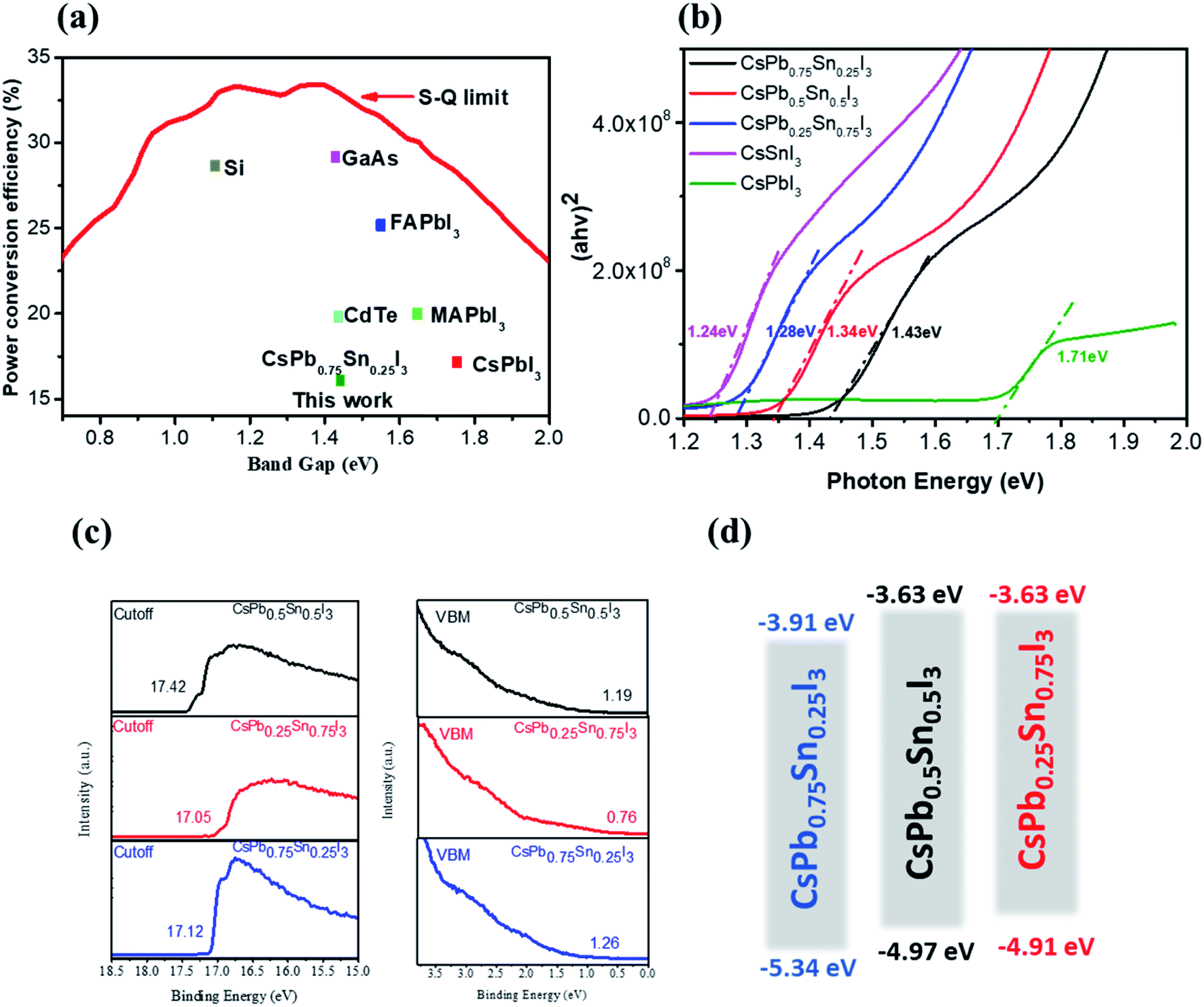 | ||
| Fig. 1 Basic properties of alloyed CsPbxSn1−xI3 inorganic perovskites. (a) Shockley–Queisser limit of CsPb0.7Sn0.3I3 perovskite and other commonly studied photovoltaic materials. (b) Tauc plot of CsPbxSn1−xI inorganic perovskites. (c) Ultraviolet photoelectron spectroscopy of CsPbxSn1−xI inorganic perovskites. (d) Band levels of CsPbxSn1−xI inorganic perovskites (valance band is estimated from ultraviolet photoelectron spectroscopy and the conduction band is calculated by subtracting the band gap estimated from Tauc plot of absorption). | ||
Table S1† gives the annealing temperatures and optical band gaps of inorganic perovskites reported in the literature, revealing the advantages of our work.
Fig. 2 shows the proposed perovskite structure and its corresponding Goldschmidt tolerance factor. In the angle of [PbxSn1−xI6]4− octahedron, the metal sites are randomly occupied by Sn or Pb atoms.41 The ionic radius of the components used here can be found in previous literature.42 As shown in Fig. 2, when the Sn content increases, the tolerance coefficient increases from 0.81 in CsPbI3 to 0.85 in CsSnI3. This result predicts that a stable Cs-based triiodide perovskite phase can be obtained due to the partial substitution of lead and tin. The increase of the empirical index indicates that the formation energy of the photoactive symmetric lattice is lower.42 For example, CsSnI3 can obtain stable photoactive phase (orthorhombic phase) at low temperature.
 | ||
| Fig. 2 Possible structures for CsPbxSn1−xI3 and their corresponding calculated Goldschmidt tolerance factor. r(Pb–Sn) is defined as the efficient radius of Pb–Sn binary based on its molar ratio. | ||
We fabricated inorganic perovskite films with lead–tin ratios of 1:0, 0.75:0.25, 0.5:0.5, 0.25:0.75, and 0:1. Fig. 3a shows 2-D X-ray diffraction (2-D XRD) patterns of CsPbxSn1−xI3 films with x being 0, 0.25, 0.5, 0.75, and 1. In the CsPbI3 films, no peaks associated with the perovskite phase can be detected in room temperature air. However, after Sn incorporation (>0.25), the characteristic peaks related to photoactive perovskite phase could be clearly observed. Interestingly, the minor features (e.g., peaks at 20.3°, 21.3°, 22.9°, 24.0°, 25.1°, and 27.1°) observed in XRD patterns of perovskite phase are in good agreement with the reported orthorhombic structure (black γ-phase) of CsSnI3.29 This result also coincides with the previous work, in which the Cs-based perovskite has small tolerance factor and lower formation energy with orthorhombic structure. To investigate further the influence of replacing with Sn2+ on crystal lattice, the zoomed-in region from 14.10° to 14.50° is displayed in Fig. 3b. As expected, with the increased Sn to Pb ratio, the diffraction peak gradually shifted to larger 2θ values, from 14.31 in CsPb0.75Sn0.25I3 to 14.40 in CsSnI3. This slight shift of peaks to larger angles is due to lattice contraction from partial replacement of Pb with Sn. To provide a visual comparison of as formed CsPbxSn1−xI3 films, atomic force microscopy was used to investigate the morphology. As shown in Fig. 3c, the grain size first decreases significantly then increases when the Sn content exceeds 50%. Moreover, the films have many pinholes, while the photoactive phase formation is observed in all films (except for CsPbI3). This result implies the smooth morphology and grain size are not the main factors for forming photoactive phase with low-temperature processing. Thus, we believe that lattice contraction is the reason for forming low-temperature photoactive phase with Sn incorporation. Fig. 3d shows the absorption spectra of CsPbxSn1−xI3 films. For CsPbI3 film under yellow phase from our low-temperature process, almost no absorption occurs beyond 600 nm. For Sn-incorporated films, a red-shifted absorption onset is observed as the Sn content (1 − x) increases. The insert in Fig. 3d is the absorption onset of the films, and the tunable optical bandgap is estimated to be 1.44 eV, 1.35 eV, and 1.28 eV for CsPb0.75Sn0.25I3, CsPb0.5Sn0.5I3, and CsPb0.25Sn0.75I3, respectively, showing their great potential as photovoltaic materials.
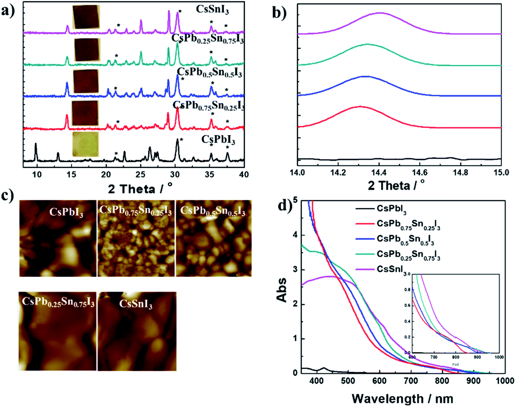 | ||
| Fig. 3 (a) Photograph of obtained CsPbxSn1−xI3 films and their 2D XRD patterns. The peaks associated with ITO are marked with asterisk. (b) Close-up 2-D XRD image of characteristic peak (∼14.3°). (c) 1 μm × 1 μm atomic force microscopy images of films. (d) The absorption spectra of CsPbxSn1−xI3 obtained by the antisolvent washing method (inserted is the absorption onset). All samples were tested in air without extra protection or encapsulation. | ||
To study the thermal stability of the films obtained, a picture of such films annealed at 150 °C in a glove box (N2) is shown in Fig. 4. We also compared the MAPbI3 films prepared under the same conditions. As shown in Fig. 4, MAPbI3 completely decomposed after 30 min, whereas CsPb0.75Sn0.25I3, CsPb0.5Sn0.5I3, CsPb0.25Sn0.75I3, and CsSnI3 did not change after 1 h. This result confirms that our CsPbxSn1−xI3 is much better than MAPbI3 in thermal stability.
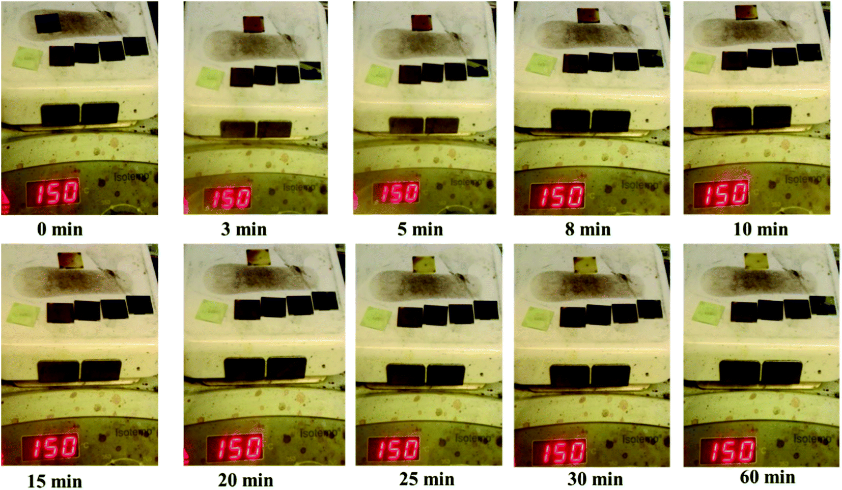 | ||
| Fig. 4 Images of perovskite films annealed at 150 °C in glove box (N2). The front row shows only MAPbI3. The second row (from left to right) shows CsPbI3, CsPb0.75Sn0.25I3, CsPb0.5Sn0.5I3, CsPb0.25Sn0.75I3, and CsSnI3. | ||
To examine the performance of devices based on these materials, devices containing CsPb0.75Sn0.25I3, CsPb0.5Sn0.5I3, and CsPb0.25Sn0.75I3 were fabricated with the configuration of ITO/PEDOT/PVSK/PCBM/bis-C60/Ag. Fig. 5a shows the corresponding photocurrent density–voltage (J–V) characteristics of devices under AM 1.5 condition. The photovoltaic parameters, open circuit voltage (VOC), short-circuit current density (JSC), fill factor (FF), and PCE are tabulated in Table 1. In the CsPb0.75Sn0.25I3 device, a PCE of 5.78% was achieved with a JSC of 15.4 mA cm−2, a VOC of 0.67 V, and a FF of 0.56 under reverse scan.
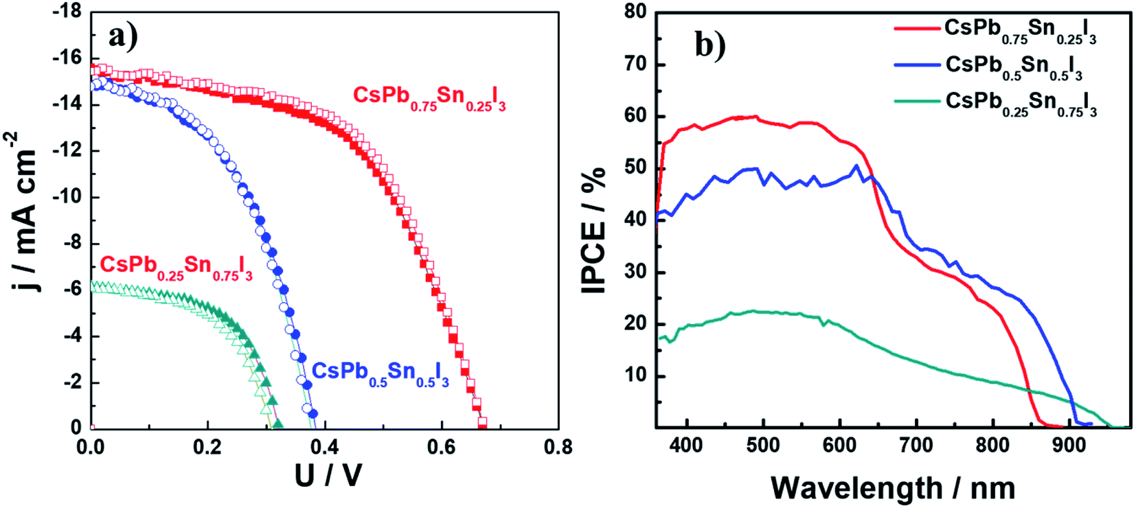 | ||
| Fig. 5 (a) The J–V curves obtained under full sun illumination for devices based on CsPb0.75Sn0.25I3, CsPb0.5Sn0.5I3, and CsPb0.25Sn0.75I3 as photoactive layers with ITO/PEDOT/PVSK/PCBM/bis-C60/Ag configuration. (b) Their incident photon-to-current conversion efficiency spectra. All the samples were tested without extra protection or encapsulation. | ||
| Photoactive layer | Scan direction | Voc/V | Jsc/mA cm−2 | FF | PCE/% |
|---|---|---|---|---|---|
| CsPb0.75Sn0.25I3 | Forward scan | 0.67 | 15.6 | 0.53 | 5.52 |
| Reverse scan | 0.67 | 15.4 | 0.56 | 5.78 | |
| CsPb0.5Sn0.5I3 | Forward scan | 0.38 | 14.8 | 0.48 | 2.72 |
| Reverse scan | 0.39 | 14.9 | 0.47 | 2.72 | |
| CsPb0.25Sn0.75I3 | Forward scan | 0.31 | 6.10 | 0.53 | 1.00 |
| Reverse scan | 0.32 | 6.20 | 0.55 | 1.10 |
However, lower PCE of 2.72% and 1.1% were observed in CsPb0.5Sn0.5I3 and CsPb0.25Sn0.75I3 devices, respectively. One possible factor for the dropped PCE is the increased recombination at sub-bandgap states due to defects caused by the oxidation of Sn2+ when the Sn content is increased.43 Nevertheless, it is interesting to point out that there is negligible hysteresis in these inorganic perovskite devices, unlike that found in FA- and MA-based Pb–Sn binary perovskite devices.43 This phenomenon coincides well with our previous finding9 that the motion of cation at A-site contributes noticeably to the hysteresis.
The incident photon-to-current conversion efficiency spectra for these devices is shown in Fig. 5b. This spectrum shows broad absorption for light harvesting, with the edge extending from 860 nm to 950 nm when the Sn content increases from 25% to 75%, which is in good agreement with the corresponding UV-vis absorption.
Conclusion
Organic–inorganic hybrid perovskite solar cells have proven to have good photoelectric properties, but large-scale production requires considerable light and thermal stability. The presence of MA+ or FA+ in organic perovskite is easy to decompose, whereas cesium-based, all-inorganic perovskite has good thermal stability. Through the co-doping of lead and tin, the photoactive phase of perovskite successfully reduced the annealing temperature to 100 °C. To sum up, a low-temperature annealing, Cs-based, all-inorganic perovskite was developed to display stable black phase. Systematic measurements show that the formation of shrinkage lattice cells by partial substitution of Sn for Pb is helpful to the realization and stabilization of photoactive perovskite phase. Through the calculation of the tolerance factor, we have successfully produced all-inorganic, lead–tin-mixed perovskite solar cells with lead-to-tin ratios of 0.75:0.25, 0.5:0.5, and 0.25:0.75. However, when the ratio of lead to tin is 0.75:0.25, the initial efficiency of all inorganic perovskite solar cells is 5.78%.
Fabrication of solar cells
ITO glass was first cleaned using detergent, followed by 10 min ultrasonication with detergent, DI water, acetone, and isopropanol, respectively. Then, the substrates were dried by nitrogen gas flow and treated with ultraviolet-ozone for 15 min before depositing PEDOT. The PEDOT/PSS solution was spin-coated onto the cleaned ITO glass substrate at 4000 rpm for 30 s and annealed at 150 °C for 15 min in air. To prepare the precursor solution of CsPbxSn1−xI3 perovskite, the CsPbI3 and CsSnI3 (with 10% ascorbic acid) precursor was made first in a mixed solvent of DMF and DMSO (4:1). Then, the 2 precursor solutions were mixed.
Afterward, a 35 μL perovskite precursor (kept at room temperature) was spin-coated onto the PEDOT layer at 4000 rpm for 35 s in the glovebox. Before spin-coating, the PEDOT substrate was kept at room temperature. Toluene (800 μL) was dripped in situ onto the substrate at the 10th s. Afterward, the perovskite films were annealed at 60 °C for 1 min and 100 °C for 4 min. PCBM solution (20 mg ml−1 in chlorobenzene) was then spin-coated onto the perovskite film at 2000 rpm for 30 s, followed by the deposition of bis-C60 layer (2 mg ml−1 in isopropyl alcohol, spin-coated at 3000 rpm for 35 s). Finally, Ag electrode with a thickness of 120 nm was evaporated under high vacuum (<2 × 10⁻⁶ torr).
Characterization
XRD was measured by X-ray diffractometer (Bruker F8 Focus Powder for regular XRD and Bruker D8 Discover 2-D XRD). SEM was measured by using FEI Sirion and operated at 5 kV. The absorption spectra were measured using a Varian Cary 5000 UV-Vis spectrometer. The J–V curves were recorded using a Keithley 2400 Source measurement unit, a 450 W xenon lamp was used to produce light, and a standard Si photodiode detector calibrated the light intensity (100 mW cm−2). The EQE spectra were measured by a joint system of monochromated 450 W xenon lamp (Oriel) and a source meter (Keithley 2400), which were calculated using a calibrated Si photodiode (OSI-Optoelectronics).Time-resolved PL decay traces were acquired using a time-correlated single photon counting system (Fluo Time 100, PicoQuant GmbH). Samples were photoexcited using a 470 nm laser beam (LDH-P-C-470, PicoQuant GmbH) pulsed at frequencies between 0.5–10 MHz, with a pulse duration of 60 ps and fluence of ∼10 nJ cm−2.
Conflicts of interest
There are no conflicts to declare.Acknowledgements
We gratefully acknowledge the Taiwanese Ministry of Science and Technology for supporting the research with the following contract numbers: MOST 108-3116-F-002-010-CC2, MOST 108-3116-F-002-009-CC2, MOST 107-2221-E-002-172-MY3.Reference
- M. M. Lee, J. Teuscher, T. Miyasaka, T. N. Murakami and H. J. Snaith, Efficient Hybrid Solar Cells Based on Meso-Superstructured Organometal Halide Perovskites, Science, 2012, 338, 643–647 CrossRef CAS.
- G. E. Eperon, S. D. Stranks, C. Menelaou, M. B. Johnston, L. M. Herz and H. J. Snaith, Formamidinium Lead Trihalide: A Broadly Tunable Perovskite for Efficient Planar Heterojunction Solar Cells, Energy Environ. Sci., 2014, 7, 982–988 RSC.
- C. C. Stoumpos, C. D. Malliakas and M. G. Kanatzidis, Semiconducting Tin and Lead Iodide Perovskites with Organic Cations: Phase Transitions, High Mobilities, and near-Infrared Photoluminescent Properties, Inorganic Chemistry, 2013, 52, 9019–9038 CrossRef CAS.
- H.-S. Kim, C.-R. Lee, J.-H. Im, K.-B. Lee, T. Moehl, A. Marchioro, S.-J. Moon, R. Humphry-Baker, J.-H. Yum and J. E. Moser, Lead Iodide Perovskite Sensitized All-Solid-State Submicron Thin Film Mesoscopic Solar Cell with Efficiency Exceeding 9%, Sci. Rep., 2012, 2, 1–7 Search PubMed.
- K. Galkowski, A. Mitioglu, A. Miyata, P. Plochocka, O. Portugall, G. E. Eperon, J. T.-W. Wang, T. Stergiopoulos, S. D. Stranks, H. Snaith and R. J. Nicholas, Energy Environ. Sci., 2016, 9, 962–970 RSC.
- A. Miyata, A. Mitioglu, P. Plochocka, O. Portugall, J. T.-W. Wang, S. D. Stranks, H. J. Snaith and R. J. Nicholas, Direct Measurement of the Exciton Binding Energy and Effective Masses for Charge Carriers in Organic–Inorganic Tri-Halide Perovskites, Nat. Phys., 2015, 11, 582–587 Search PubMed.
- S. D. Stranks, G. E. Eperon, G. Grancini, C. Menelaou, M. J. Alcocer, T. Leijtens, L. M. Herz, A. Petrozza and H. J. Snaith, Electron-Hole Diffusion Lengths Exceeding 1 Micrometer in an Organometal Trihalide Perovskite Absorber, Science, 2013, 342, 341–344 CrossRef CAS.
- G. Xing, N. Mathews, S. Sun, S. S. Lim, Y. M. Lam, M. Grätzel, S. Mhaisalkar and T. C. Sum, Long-Range Balanced Electron-and Hole-Transport Lengths in Organic–Inorganic CH3NH3PbI3, Science, 2013, 342, 344–347 CrossRef CAS.
- X. Xu and M. Wang, Photocurrent Hysteresis Related to Ion Motion in Metal–Organic Perovskites, Sci. China: Chem., 2017, 60, 396–404 CrossRef CAS.
- J. P. Correa-Baena, A. Abate, M. Saliba, W. Tress, T. j. Jacobsson, M. Gratzel and A. Hagfeldt, Energy Environ. Sci., 2017, 10, 710 RSC.
- A. Kojima, K. Teshima, Y. Shirai and T. Miyasaka, Organometal Halide Perovskites as Visible-Light Sensitizers for Photovoltaic Cells, J. Am. Chem. Soc., 2009, 131, 6050–6051 CrossRef CAS.
- E. J. Juarez-Perez, Z. Hawash, S. R. Raga, L. K. Ono and Y. Qi, Thermal Degradation of CH3NH3PbI3 Perovskite into NH3 and CH3I Gases Observed by Coupled Thermogravimetry–Mass Spectrometry Analysis, Energy Environ. Sci., 2016, 9, 3406–3410 RSC.
- M. Saliba, T. Matsui, J.-Y. Seo, K. Domanski, J.-P. Correa-Baena, M. K. Nazeeruddin, S. M. Zakeeruddin, W. Tress, A. Abate and A. Hagfeldt, Cesium-Containing Triple Cation Perovskite Solar Cells: Improved Stability, Reproducibility and High Efficiency, Energy Environ. Sci., 2016, 9, 1989–1997 RSC.
- T. Leijtens, G. E. Eperon, S. Pathak, A. Abate, M. M. Lee and H. J. Snaith, Overcoming Ultraviolet Light Instability of Sensitized TIO2 with Meso-Superstructured Organometal Tri-Halide Perovskite Solar Cells, Nat. Commun., 2013, 4, 1–8 Search PubMed.
- Y. Chen, T. Chen and L. Dai, Layer-by-Layer Growth of CH3NH3PbI3−xClx for Highly Efficient Planar Heterojunction Perovskite Solar Cells, Adv. Mater., 2015, 27, 1053–1059 CrossRef CAS.
- N. Aristidou, I. Sanchez-Molina, T. Chotchuangchutchaval, M. Brown, L. Martinez, T. Rath and S. A. Haque, The Role of Oxygen in the Degradation of Methylammonium Lead Trihalide Perovskite Photoactive Layers, Angew. Chem., 2015, 127, 8326–8330 CrossRef.
- J. A. Christians, P. A. Miranda Herrera and P. V. Kamat, Transformation of the Excited State and Photovoltaic Efficiency of CH3NH3PbI3 Perovskite Upon Controlled Exposure to Humidified Air, J. Am. Chem. Soc., 2015, 137, 1530–1538 CrossRef CAS.
- J. Yang, B. D. Siempelkamp, D. Liu and T. L. Kelly, Investigation of CH3NH3PbI3 Degradation Rates and Mechanisms in Controlled Humidity Environments Using in Situ Techniques, ACS Nano, 2015, 9, 1955–1963 CrossRef CAS.
- L. Zhao, J. Gao, Y. L. Lin, Y. W. Yeh, K. M. Lee, N. Yao, Y. L. Loo and B. P. Rand, Electrical Stress Influences the Efficiency of CH3NH3PbI3 Perovskite Light Emitting Devices, Adv. Mater., 2017, 29, 1605317 CrossRef.
- Z. Xiao, Y. Yuan, Y. Shao, Q. Wang, Q. Dong, C. Bi, P. Sharma, A. Gruverman and J. Huang, Giant Switchable Photovoltaic Effect in Organometal Trihalide Perovskite Devices, Nat. Mater., 2015, 14, 193–198 CrossRef CAS.
- I. Deretzis and A. La Magna, Exploring the Orthorhombic–Tetragonal Phase Transition in CH3NH3PbI3: The Role of Atom Kinetics, Nanoscale, 2017, 9, 5896–5903 RSC.
- B. Conings, J. Drijkoningen, N. Gauquelin, A. Babayigit, J. D'Haen, L. D'Olieslaeger, A. Ethirajan, J. Verbeeck, J. Manca and E. Mosconi, Intrinsic Thermal Instability of Methylammonium Lead Trihalide Perovskite, Adv. Energy Mater., 2015, 5, 1500477 CrossRef.
- T. A. Berhe, W.-N. Su, C.-H. Chen, C.-J. Pan, J.-H. Cheng, H.-M. Chen, M.-C. Tsai, L.-Y. Chen, A. A. Dubale and B.-J. Hwang, Organometal Halide Perovskite Solar Cells: Degradation and Stability, Energy Environ. Sci., 2016, 9, 323–356 RSC.
- J. Huang, P. Xu, J. Liu and X. Z. You, Sequential Introduction of Cations Deriving Large-Grain CsxFA1−xPbI3 Thin Film for Planar Hybrid Solar Cells: Insight into Phase-Segregation and Thermal-Healing Behavior, Small, 2017, 13, 1603225 CrossRef.
- M. Grätzel, The Rise of Highly Efficient and Stable Perovskite Solar Cells, Acc. Chem. Res., 2017, 50, 487–491 CrossRef.
- N. J. Jeon, J. H. Noh, W. S. Yang, Y. C. Kim, S. Ryu, J. Seo and S. I. Seok, Compositional Engineering of Perovskite Materials for High-Performance Solar Cells, Nature, 2015, 517, 476–480 CrossRef CAS.
- X. Xu, Q. Chen, Z. Hong, H. Zhou, Z. Liu, W.-H. Chang, P. Sun, H. Chen, N. D. Marco and M. Wang, Working Mechanism for Flexible Perovskite Solar Cells with Simplified Architecture, Nano Lett., 2015, 15, 6514–6520 CrossRef CAS.
- P. Wang, X. Zhang, Y. Zhou, Q. Jiang, Q. Ye, Z. Chu, X. Li, X. Yang, Z. Yin and J. You, Solvent-Controlled Growth of Inorganic Perovskite Films in Dry Environment for Efficient and Stable Solar Cells, Nat. Commun., 2018, 9, 1–7 CrossRef.
- I. Chung, J.-H. Song, J. Im, J. Androulakis, C. D. Malliakas, H. Li, A. J. Freeman, J. T. Kenney and M. G. Kanatzidis, CsSnI3: Semiconductor or Metal? High Electrical Conductivity and Strong near-Infrared Photoluminescence from a Single Material. High Hole Mobility and Phase-Transitions, J. Am. Chem. Soc., 2012, 134, 8579–8587 CrossRef CAS.
- A. Swarnkar, A. R. Marshall, E. M. Sanehira, B. D. Chernomordik, D. T. Moore, J. A. Christians, T. Chakrabarti and J. M. Luther, Quantum Dot–Induced Phase Stabilization of Α-CsPbI3 Perovskite for High-Efficiency Photovoltaics, Science, 2016, 354, 92–95 CrossRef CAS.
- R. J. Sutton, G. E. Eperon, L. Miranda, E. S. Parrott, B. A. Kamino, J. B. Patel, M. T. Hörantner, M. B. Johnston, A. A. Haghighirad and D. T. Moore, Bandgap-Tunable Cesium Lead Halide Perovskites with High Thermal Stability for Efficient Solar Cells, Adv. Energy Mater., 2016, 6, 1502458 CrossRef.
- R. E. Beal, D. J. Slotcavage, T. Leijtens, A. R. Bowring, R. A. Belisle, W. H. Nguyen, G. F. Burkhard, E. T. Hoke and M. D. McGehee, Cesium Lead Halide Perovskites with Improved Stability for Tandem Solar Cells, J. Phys. Chem. Lett., 2016, 7, 746–751 CrossRef CAS.
- C. Y. Chen, H. Y. Lin, K. M. Chiang, W. L. Tsai, Y. C. Huang, C. S. Tsao and H. W. Lin, All-Vacuum-Deposited Stoichiometrically Balanced Inorganic Cesium Lead Halide Perovskite Solar Cells with Stabilized Efficiency Exceeding 11%, Adv. Mater., 2017, 29, 1605290 CrossRef.
- J. K. Nam, M. S. Jung, S. U. Chai, Y. J. Choi, D. Kim and J. H. Park, Unveiling the Crystal Formation of Cesium Lead Mixed-Halide Perovskites for Efficient and Stable Solar Cells, J. Phys. Chem. Lett., 2017, 8, 2936–2940 CrossRef CAS.
- H. Queisser, Slip Patterns on Boron-Doped Silicon Surfaces, J. Appl. Phys., 1961, 32, 1776–1780 CrossRef CAS.
- Y. Wang, M. I. Dar, L. K. Ono, T. Zhang, M. Kan, Y. Li, L. Zhang, X. Wang, Y. Yang and X. Gao, Thermodynamically Stabilized Β-CsPbI3-Based Perovskite Solar Cells with Efficiencies >18%, Science, 2019, 365, 591–595 CrossRef CAS.
- J. Lin, M. Lai, L. Dou, C. S. Kley, H. Chen, F. Peng, J. Sun, D. Lu, S. A. Hawks and C. Xie, Thermochromic Halide Perovskite Solar Cells, Nat. Mater., 2018, 17, 261–267 CrossRef CAS.
- J. A. Steele, H. Jin, I. Dovgaliuk, R. F. Berger, T. Braeckevelt, H. Yuan, C. Martin, E. Solano, K. Lejaeghere and S. M. Rogge, Thermal Unequilibrium of Strained Black CsPbI3 Thin Films, Science, 2019, 365, 679–684 CrossRef CAS.
- T. Wu, Y. Wang, Z. Dai, D. Cui, T. Wang, X. Meng, E. Bi, X. Yang and L. Han, Efficient and Stable CsPbI3 Solar Cells Via Regulating Lattice Distortion with Surface Organic Terminal Groups, Adv. Mater., 2019, 31, 1900605 CrossRef.
- W. Shockley and H. J. Queisser, Detailed Balance Limit of Efficiency of P–N Junction Solar Cells, J. Appl. Phys., 1961, 32, 510–519 CrossRef CAS.
- F. Hao, C. C. Stoumpos, R. P. Chang and M. G. Kanatzidis, Anomalous Band Gap Behavior in Mixed Sn and Pb Perovskites Enables Broadening of Absorption Spectrum in Solar Cells, J. Am. Chem. Soc., 2014, 136, 8094–8099 CrossRef CAS.
- A. Amat, E. Mosconi, E. Ronca, C. Quarti, P. Umari, M. K. Nazeeruddin, M. Gratzel and F. De Angelis, Cation-Induced Band-Gap Tuning in Organohalide Perovskites: Interplay of Spin–Orbit Coupling and Octahedra Tilting, Nano Lett., 2014, 14, 3608–3616 CrossRef CAS.
- X. Xu, C.-C. Chueh, Z. Yang, A. Rajagopal, J. Xu, S. B. Jo and A. K.-Y. Jen, Ascorbic Acid as an Effective Antioxidant Additive to Enhance the Efficiency and Stability of Pb/Sn-Based Binary Perovskite Solar Cells, Nano Energy, 2017, 34, 392–398 CrossRef CAS.
- X. Chen, Z. Jia, Z. Chen, T. Jiang, L. Bai, F. Tao, J. Chen, X. Chen, T. Liu, X. Xu, C. Yang, W. Shen, W. E. I. Sha, H. Zhu and Y. M. Yang, Efficient and Reproducible Monolithic Perovskite/Organic Tandem Solar Cells with Low-Loss Interconnecting Layers, Joule, 2020, 4(7), 1594–1606 CrossRef CAS.
- W. Zhu, W. Ma, Y. Su, Z. Chen, X. Chen, Y. Ma, L. Bai, W. Xiao, T. Liu, H. Zhu, X. Liu, H. Liu, X. Liu and Y. M. Yang, Low-dose real-time X-ray imaging with nontoxic double perovskite scintillators, Light: Sci. Appl., 2020, 9(1), 112 CrossRef CAS.
- T. Jiang, Z. Chen, X. Chen, T. Liu, X. Chen, W. E. I. Sha, H. Zhu and Y. M. Yang, Realizing High Efficiency over 20% of Low-Bandgap Pb–Sn-Alloyed Perovskite Solar Cells by In Situ Reduction of Sn 4+, Sol. RRL, 2019, 4(3), 1900467 CrossRef.
- R. Zhuang, X. Wang, W. Ma, Y. Wu, X. Chen, L. Tang, H. Zhu, J. Liu, L. Wu, W. Zhou, X. Liu and Y. M. Yang, Highly sensitive X-ray detector made of layered perovskite-like (NH4)3Bi2I9 single crystal with anisotropic response, Nat. Photonics, 2019, 13(9), 602–608 CrossRef CAS.
Footnote |
| † Electronic supplementary information (ESI) available. See DOI: 10.1039/d0ra10110a |
| This journal is © The Royal Society of Chemistry 2021 |