DOI:
10.1039/D0RA10075G
(Paper)
RSC Adv., 2021,
11, 8033-8041
N-type and p-type molecular doping on monolayer MoS2†
Received
29th November 2020
, Accepted 15th February 2021
First published on 18th February 2021
Abstract
Monolayer MoS2 has attracted much attention due to its high on/off current ratio, transparency, and suitability for optoelectronic devices. Surface doping by molecular adsorption has proven to be an effective method to facilitate the usage of MoS2. However, there are no works available to systematically clarify the effects of the adsorption of F4TCNQ, PTCDA, and tetracene on the electronic and optical properties of the material. Therefore, this work elucidated the problem by using density functional theory calculations. We found that the adsorption of F4TCNQ and PTCDA turns MoS2 into a p-type semiconductor, while the tetracene converts MoS2 into an n-type semiconductor. The occurrence of a new energy level in the conduction band for F4TCNQ and PTCDA and the valence band for tetracene reduces the bandgap of the monolayer MoS2. Besides, the MoS2/F4TCNQ and MoS2/PTCDA systems exhibit an auxiliary optical peak at the long wavelengths of 950 and 850 nm, respectively. Contrastingly, the MoS2/tetracene modifies the optical spectrum of the monolayer MoS2 only in the ultraviolet region. The findings are in good agreement with the experiments.
1. Introduction
The monolayer MoS2 is a semiconducting transition metal dichalcogenide with an optical bandgap of about 1.8 eV. This material has proven to possess high on/off current ratio and transparency, making it suitable for electronic and optoelectronic applications.1,2 The properties of monolayer MoS2 are adjustable by modifying the crystal structure, doping with different elements, and the adsorption of organic molecules.3–6 The application of organic molecular adsorption is attractive because of advantages such as mechanical flexibility, easy fabrication, light weight, and low cost.7,8 Organic molecular adsorption has been demonstrated as a viable method to optimize material properties,6 also to protect MoS2 from oxidation under ambient conditions.9 Therefore, it is essential to understand the behavior of the organic adsorption on the monolayer MoS2 to optimize its performance for optoelectronic uses.
Here, we studied the adsorption of three organic molecules, i.e., 2,3,5,6-tetrafluoro-7,7,8,8-tetracyanoquinodimethane (F4TCNQ), perylene-3,4,9,10-tetracarboxylic dianhydride (PTCDA), and tetracene. Where, F4TCNQ is one of the most effective p-type dopants due to its strong ability of electron acceptance.10–13 The experiment showed that F4TCNQ could modify the electrical and optical properties of MoS2.11 Hu et al. confirmed that the deposition of F4TCNQ on the monolayer MoS2 allows convenient control of the radioactive exciton recombination for laser and LED applications.12 The charge transfer within the F4TCNQ–MoS2 interface can tune electrical and gas sensing properties.13 PTCDA and tetracene are popular organic semiconductors that have attracted many research interests in the past decades.8,14–19 Tetracene was used for field-effect transistors.20,21 The study of Habib showed the outstanding luminescent properties of the MoS2/PTCDA system.17 Also, Wang et al. have demonstrated the novel MoS2/PTCDA hybrid heterojunction synapse transistor with both electrical and optical modulation and efficient gate tunability.18 Besides, the MoS2/tetracene is a good candidate for the anti-ambipolar field-effect transistor.21
The literature review showed that most of the available research is experiments, and there is no theoretical study available to elucidate the interaction between the MoS2 monolayer and the mentioned organic molecules. Therefore, this work is going to clarify it by using the density functional theory (DFT) method and analyzing the electronic structure and optical properties of MoS2 without and with the adsorption of F4TCNQ, PTCDA, and tetracene. Furthermore, this work also considers the influences of pressure on the properties.
2. Computational method
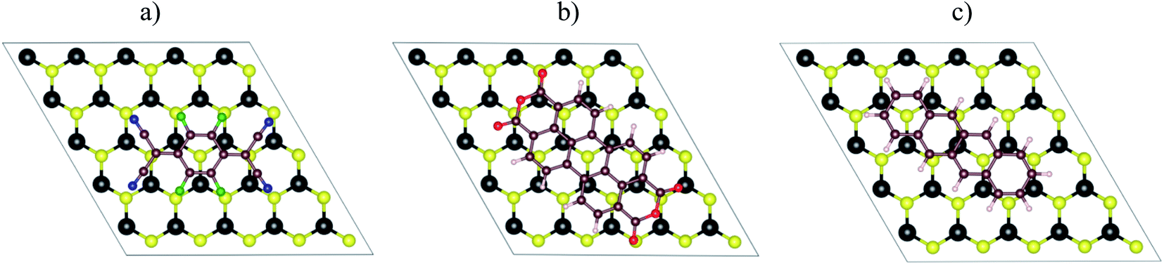
Fig. 1a–c visualized the molecular structure of F4TCNQ (C12F4N4), PTCDA (C24H8O6), and tetracene (C18H12), respectively. The monolayer MoS2, shown in Fig. 1d, was described by a slab model with the 5 × 5 unit cell and a vacuum space of 27 Å along the normal direction of the MoS2 surface.
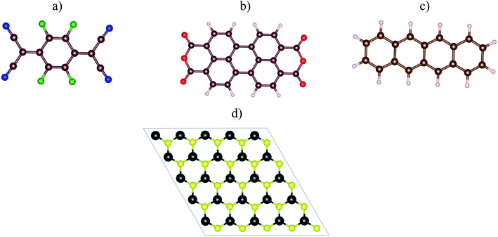 |
| | Fig. 1 The top view of organic molecules: (a) F4TCNQ, (b) PTCDA, (c) tetracene, and (d) the monolayer MoS2. Blue (N), green (F), brown (C), red (O), white (H), yellow (S), and black (Mo). | |
The optimized geometry structure and total energy of the monolayer MoS2 with organic molecular adsorption were obtained with the aid of the Vienna ab initio simulation package (VASP).22–24 The projector-augmented-wave method was used to describe the valence electron–core ion interaction.25,26 The electron exchange–correlation interactions were treated by using the PBE-GGA approximation of the Perdew–Burke–Ernzerhof,27,28 which has shown to be a reasonable approximation for the bandgap of the monolayer MoS2.29 The plane-wave cutoff energy was 600 eV. The k-point mesh was sampled at 3 × 3 × 1 in the first Brillouin zone by Monkhorst–Pack technique.30 All atomic positions of MoS2 and MoS2/organic-molecule systems are fully relaxed during the geometry optimization until the interatomic forces meeting the upper criterion of 0.001 eV Å−1.
The pressure applying to the system is defined by
| |
 | (1) |
where, the energy and volume of the strained (unstrained) system are denoted as
E and
V (
E0 and
V0), respectively. The volume of the unit cell of the monolayer MoS
2 is

(
a is the lattice constant and
c is the thickness of the slab). The pressure is modified by changing the lattice constant
a =
b.
The adsorption energy of F4TCNQ, PTCDA, and tetracene on the monolayer MoS2 is calculated by
| | |
Ea = Esub+om − (Esub + Eom),
| (2) |
where,
Esub+om,
Esub, and
Eom are the total energy of the MoS
2/organic molecule system, the isolated monolayer MoS
2, and the isolated organic molecule, respectively.
The optical property of the systems was determined through the imaginary part ε(ω) of dielectric constant, which is calculated by the summation over empty states as follows:31,32
| |
 | (3) |
here,
ω is the frequency of emission,
ε0 is the dielectric constant of free space. The valence and conduction band wave functions are
ξvk and
ξck, respectively. The unit cell volume is
V, and the polarization vector of the electric field of the emission is
![[v with combining circumflex]](https://www.rsc.org/images/entities/i_char_0076_0302.gif)
.
3. Results and discussion
3.1. Structural properties
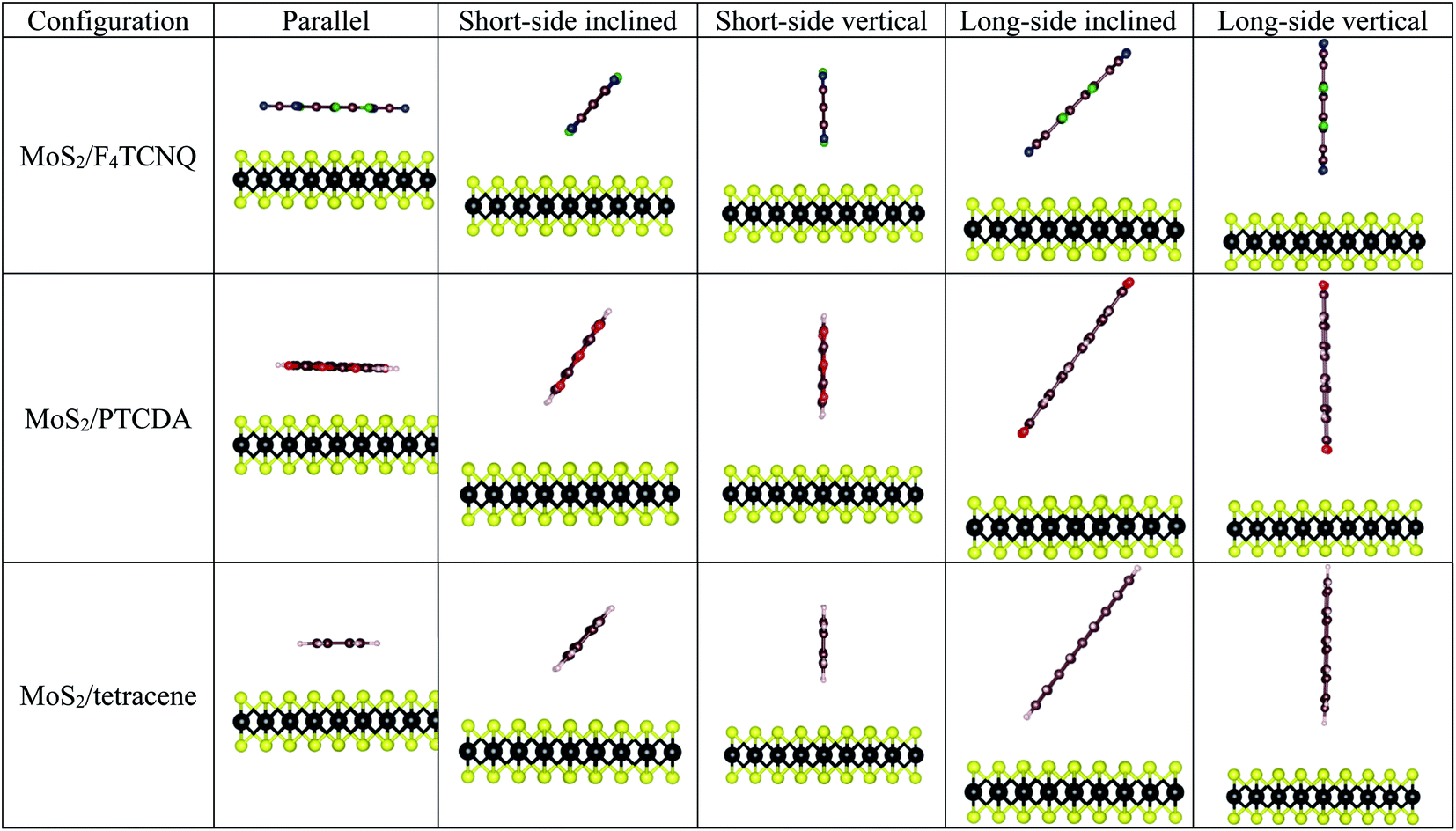
The optimized structural parameters for the monolayer MoS2 were obtained in the previous publication,33 where the optimized lattice constant was found to be a = b = 3.18 Å. To explore the adsorption properties of F4TCNQ, PTCDA, and tetracene on the monolayer MoS2, the geometry of the organic molecules with different configurations was optimized at several adsorption sites on the surface of MoS2 as shown in Fig. 2. The most favorable adsorption of the F4TCNQ, PTCDA, and tetracene molecules on the MoS2 substrate was obtained for the short-side inclined configuration based on the most negative adsorption energy listed in Table 1.
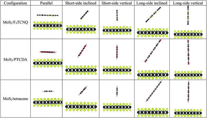 |
| | Fig. 2 The side view of the possible adsorption configurations of F4TCNQ, PTCDA, and tetracene on the monolayer MoS2. | |
Table 1 Adsorption energy Ea (eV) for different configurations on the monolayer MoS2 without strain
| Adsorption configuration |
F4TCNQ |
PTCDA |
Tetracene |
| Parallel |
−0.009 |
0.019 |
0.039 |
| Short-side inclined |
−0.055 |
−0.071 |
−0.046 |
| Short-side vertical |
−0.038 |
−0.036 |
−0.030 |
| Long-side inclined |
−0.027 |
−0.031 |
−0.022 |
| Long-side vertical |
−0.023 |
−0.17 |
0.137 |
Although the adsorption energy of the short-side inclined and parallel configurations are different, the electronic density of states (DOS) and the dielectric function are almost the same, as shown in Fig. S1 and S2 in the ESI.† Therefore, to make a comparison with the previous publication on polyethyleneimine,33 we will perform a detailed analysis of the geometrical structure, the DOS, and the dielectric function for the parallel configuration of F4TCNQ, PTCDA, and tetracene. Furthermore, we also found that the extension of the unit cell size to 6 × 6 and the inclusion of van der Waals correction (using vdW-DF functional) generated more negative adsorption energy (Tables S1 and S2†). However, the electronic structure of the MoS2/F4TCNQ, MoS2/PTCDA, and MoS2/tetracene systems remain the same as that of the unit cell 5 × 5 without van der Waals correction, as shown in Fig. S3.† Thus, it is acceptable to select the unit cell 5 × 5 and the PBE-GGA approximation in the present study.
Table 2 listed the adsorption energy and the vertical nearest distance to the MoS2 surface of the F4TCNQ, PTCDA, and tetracene molecules in the parallel configuration (Fig. 3). With the application of the tensile strain to the system, the organic molecules become stabilized with more negative adsorption energy relative to that at the lattice constant of 3.18 Å (without strain). The compressive pressure makes the molecules less stable with more positive adsorption energy. Table 2 also shows that the vertical nearest distance to the surface increases with the increase of the lattice constant. This result seems contradicted to the tendency of the more stable configuration of the adsorption upon modifying the tensile strain. Although the vertical nearest distance increases, the electrostatically attractive force between the adsorbates and MoS2 increases at a faster rate.33 Therefore, the adsorption energy becomes more negative. Besides, the interaction of the molecules with the surface is physisorption.
Table 2 Adsorption energy Ea and the shortest distance d from the organic molecule to the substrate surface
| aa (Å) |
MoS2/F4TCNQ |
MoS2/PTCDA |
MoS2/tetracene |
| Ea (eV) |
d (Å) |
Ea (eV) |
d (Å) |
Ea (eV) |
d (Å) |
| 2.84 and 3.00 Å: for compressive pressure; 3.18 Å: without pressure; 3.32, 3.48, and 3.64 Å: for tensile strain. |
| 2.84 |
0.034 |
3.44 |
0.095 |
3.48 |
0.105 |
3.49 |
| 3.00 |
0.066 |
3.41 |
0.098 |
3.46 |
0.092 |
3.41 |
| 3.18 |
−0.009 |
3.47 |
0.019 |
3.53 |
0.039 |
3.49 |
| 3.32 |
−0.090 |
3.58 |
−0.019 |
3.60 |
−0.018 |
3.58 |
| 3.48 |
−0.130 |
3.60 |
−0.074 |
3.64 |
−0.128 |
3.61 |
| 3.64 |
−0.145 |
3.77 |
−0.080 |
3.79 |
−0.230 |
3.72 |
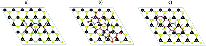 |
| | Fig. 3 The top view of the parallel adsorption configuration of the organic molecules on the monolayer MoS2: (a) F4TCNQ, (b) PTCDA, and (c) tetracene. | |
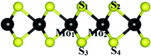 |
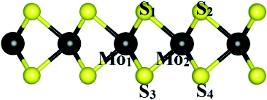
| | Fig. 4 The index of atoms for the bond lengths and angles. | |
The geometrical parameters such as the bond length and bond angle of the MoS2 substrate before and after the adsorption of the organic molecules are exhibited in Table 3. We found that the structural parameters did not change significantly after the adsorption of the molecules, which is consistent with the physical adsorption found in this work.
Table 3 Structural parameters of the MoS2 substrate before and after the adsorption of the organic molecules. The index of atoms is described in Fig. 4
| Parameters |
MoS2 |
MoS2/F4TCNQ |
MoS2/PTCDA |
MoS2/tetracene |
| Bonds (Å) |
S1–S2 |
3.183 |
3.160 |
3.162 |
3.160 |
| S1–S3 |
3.126 |
3.144 |
3.146 |
3.132 |
| Mo1–Mo2 |
3.187 |
3.183 |
3.180 |
3.182 |
| Mo2–S1 |
2.415 |
2.415 |
2.415 |
2.413 |
| Angles (°) |
Mo1S1Mo2 |
82.30 |
82.46 |
82.34 |
82.52 |
| S1Mo2S2 |
82.30 |
81.76 |
81.88 |
81.84 |
| S1Mo1S3 |
80.54 |
80.90 |
81.02 |
80.78 |
3.2. Electronic properties
Fig. 5 presents the band structure of MoS2 before and after the adsorption of F4TCNQ, PTCDA, and tetracene at zero pressure. The bandgap is determined by the difference between the conduction band minimum and the valence band maximum. We find that the isolated substrate shows a direct bandgap of 1.68 eV at the K point, as listed in Table 4. The calculated bandgap of 1.68 eV comes from the electronic contribution only, while the experimental value of 1.80 eV has included the exciton binding energy.2,3,34 Upon the adsorption of the organic molecules, the new energy state occurs in the bandgap region of the MoS2 substrate. The new energy level occurring above the Fermi level for the adsorption of F4TCNQ and PTCDA implies that the substrate became the p-type semiconductor. Whilst, it occurring below the Fermi level for the adsorption of tetracene indicates that the monolayer MoS2 became the n-type semiconductor. The existence of the new energy level shrinks the bandgap of the MoS2 to 0.36, 1.43, and 0.72 eV for the adsorption of F4TCNQ, PTCDA, and tetracene, respectively. However, the bandgap of the MoS2 remains the direct bandgap nature after the adsorption of the organic molecules.
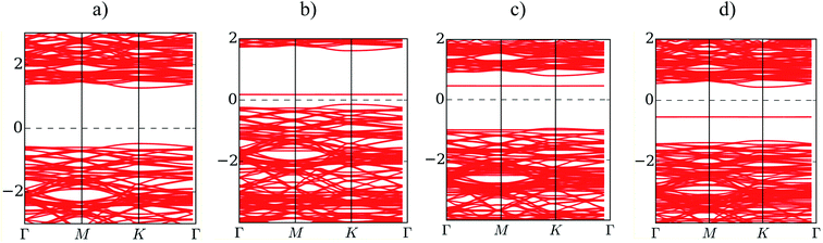 |
| | Fig. 5 The electronic band structure of (a) the monolayer MoS2, (b) MoS2/F4TCNQ, (c) MoS2/PTCDA, and (d) MoS2/tetracene at zero pressure. | |
Table 4 The bandgap Eg of the monolayer MoS2 with and without the adsorption of the organic molecules
| a (Å) |
MoS2a |
MoS2/F4TCNQ |
MoS2/PTCDA |
MoS2/tetracene |
| P (GPa) |
Eg (eV) |
P (GPa) |
Eg (eV) |
P (GPa) |
Eg (eV) |
P (GPa) |
Eg (eV) |
| In ref. 33. |
| 2.84 |
−56.18 |
1.05 |
−57.93 |
0.01 |
−60.27 |
0.93 |
−56.61 |
0.55 |
| 3.00 |
−32.44 |
1.55 |
−25.03 |
0.29 |
−32.70 |
1.20 |
−35.46 |
0.82 |
| 3.04 |
−27.65 |
1.72 |
−20.31 |
0.31 |
−20.74 |
1.25 |
−22.88 |
0.85 |
| 3.12 |
−10.69 |
1.80 |
−7.64 |
0.34 |
−7.93 |
1.37 |
−7.78 |
0.87 |
| 3.16 |
−9.46 |
1.75 |
−1.79 |
0.35 |
−1.91 |
1.41 |
−2.24 |
0.74 |
| 3.18 |
0 |
1.68 |
0 |
0.36 |
0 |
1.43 |
0 |
0.72 |
| 3.32 |
10.13 |
0.81 |
12.21 |
0.22 |
12.57 |
0.81 |
11.68 |
0.22 |
| 3.48 |
24.95 |
0 |
22.59 |
0 |
22.41 |
0 |
23.03 |
0 |
| 3.64 |
41.14 |
0 |
35.36 |
0 |
37.26 |
0 |
29.44 |
0 |
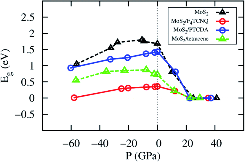
The change of the lattice constant modifies the pressure applied to the system. The details of the bandgap and the pressure are described in Table 4 and visualized in Fig. 6. We found that the bandgap behavior of MoS2/tetracene is similar to that of the monolayer MoS2, which exhibits a concave-downward curve with the maximum bandgap of 0.87 and 1.80 eV found at the pressure of −7.78 and −10.69 GPa for the MoS2/tetracene and monolayer MoS2, respectively. The concave-downward curve for the bandgap versus the pressure for the MoS2 system was found to be in good agreement with experiment,35 while that for the MoS2/tetracene is similar to that of an n-type semiconductor, the MoS2/PEI interface, in the previous study.33,36 There is a little difference in the behavior of the bandgap versus the pressure for MoS2/F4TCNQ and MoS2/PTCDA compared to that of the monolayer MoS2. That is the bandgap somehow linearly increases to a maximum value and then decreases with more positive pressures. The maximum value is 0.36 and 1.43 eV at the zero pressure for MoS2/F4TCNQ and MoS2/PTCDA, respectively. We have to impress that MoS2/F4TCNQ and MoS2/PTCDA are the p-type semiconductors, which are different from the n-type of the MoS2/tetracene. The monolayer MoS2, MoS2/F4TCNQ, MoS2/PTCDA, and MoS2/tetracene were found to be completely converted to the metal with the bandgap of 0 eV at the pressure of 24.95, 22.59, 22.41, and 23.03 GPa, respectively.
 |
| | Fig. 6 The bandgap versus pressure of the monolayer MoS2 with and without the adsorption of the organic molecules. | |
In a complex structure, the Bader point charge of an atom was determined in two steps: (1) calculating the charge by the Bader partition technique, and (2) subtracting the charge obtained in step (1) to that of the neutral atom. In the pseudopotential method of the DFT, one considers the contribution of valence electrons only. Table 5 presents the minus–plus signs as the loss and gain of charge, respectively. We found that F4TCNQ and PTCDA accept while MoS2 donates the charge. Contrastingly, the tetracene donates while MoS2 gains the charge. These results are in a good correlation with the p-type doping nature of F4TCNQ and PTCDA and the n-type doping of tetracene on the MoS2 monolayer.
Table 5 The point charge (in the unit of e) of the MoS2/F4TCNQ, MoS2/PTCDA, and MoS2/tetracene systems
| MoS2/F4TCNQ |
| P (GPa) |
MoS2 |
F4TCNQ |
| −57.93 |
−0.226 |
+0.226 |
| −25.03 |
−0.098 |
+0.098 |
| 0 |
−0.073 |
+0.073 |
| 12.21 |
−0.144 |
+0.144 |
| 22.59 |
−0.231 |
+0.231 |
| MoS2/PTCDA |
| P (GPa) |
MoS2 |
PTCDA |
| 23.03 |
−0.015 |
+0.015 |
| 29.44 |
−0.017 |
+0.017 |
| −20.74 |
−0.019 |
+0.019 |
| 0 |
−0.020 |
+0.020 |
| 12.57 |
−0.021 |
+0.021 |
| 22.41 |
−0.025 |
+0.025 |
| MoS2/tetracene |
| P (GPa) |
MoS2 |
Tetracene |
| −56.61 |
+0.062 |
−0.062 |
| −35.46 |
+0.060 |
−0.060 |
| −22.88 |
+0.052 |
−0.052 |
| −7.78 |
+0.045 |
−0.045 |
| 0 |
+0.048 |
−0.048 |
| 11.68 |
+0.050 |
−0.050 |
| 23.03 |
+0.103 |
−0.103 |
| 29.44 |
+0.363 |
−0.363 |
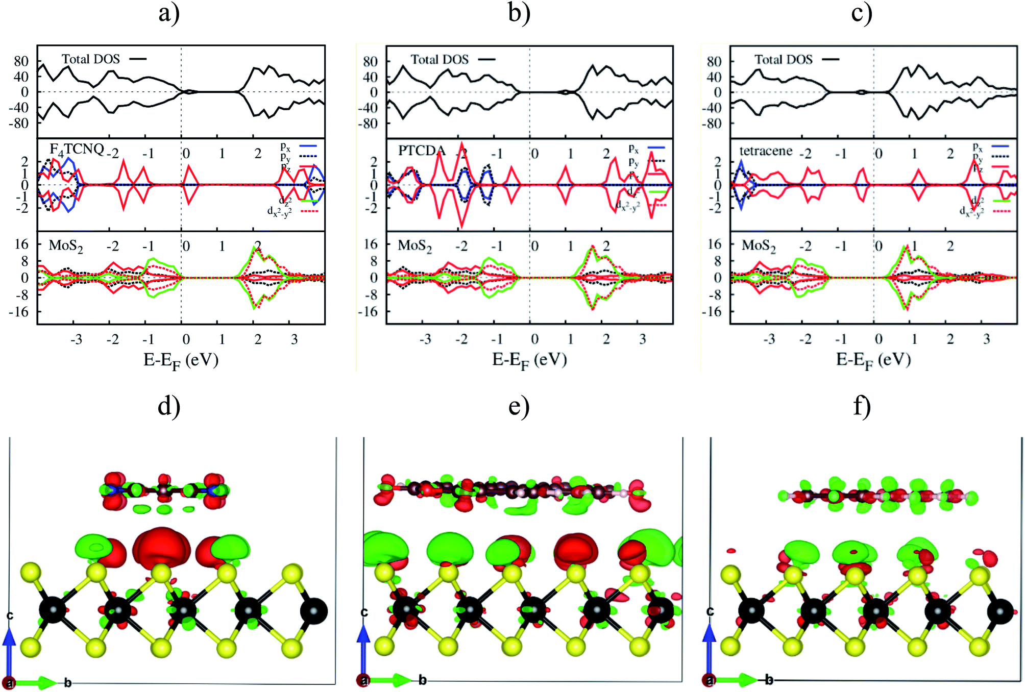
The electronic density of states (DOS) in Fig. 7a–c shows that the adsorption of F4TCNQ, PTCDA, and tetracene contributes to the appearance of the new state coming from the pz orbital of the organic molecules. As shown in Fig. 7d–f, the charge clouds of the atoms of the organic molecules clearly show the shape of pz orbitals along the vertical direction, the vector c. The charge accumulation was found to more dominant on the F4TCNQ and PTCDA, while the charge donation distributes more on tetracene. This result is in agreement with the above analysis about the Bader charge.
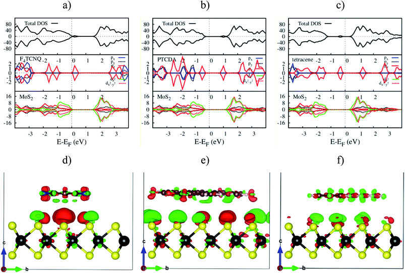 |
| | Fig. 7 The upper panel is the total and orbital-projected DOS. The bottom panel is the charge density difference at zero pressure. From left to right is for MoS2/F4TCNQ, MoS2/PTCDA, and MoS2/tetracene, respectively. Occupied and unoccupied states are presented in red and green in that order. | |
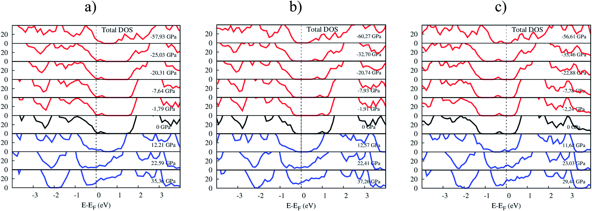
Fig. 8 shows the response of the total electronic density of states toward the influence of pressure. The p-type doping F4TCNQ and PTCDA shift the valence band maximum of MoS2 upward, while the n-type doping tetracene moves the conduction band minimum of MoS2 downward near to the Fermi level. The variation of the position of the valence band maximum and conduction band minimum leads to modifying the bandgap of the systems.
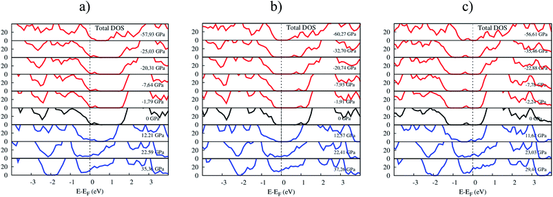 |
| | Fig. 8 The total DOS of (a) MoS2/F4TCNQ, (b) MoS2/PTCDA, and (c) MoS2/tetracene under pressure. | |
3.3. Optical properties
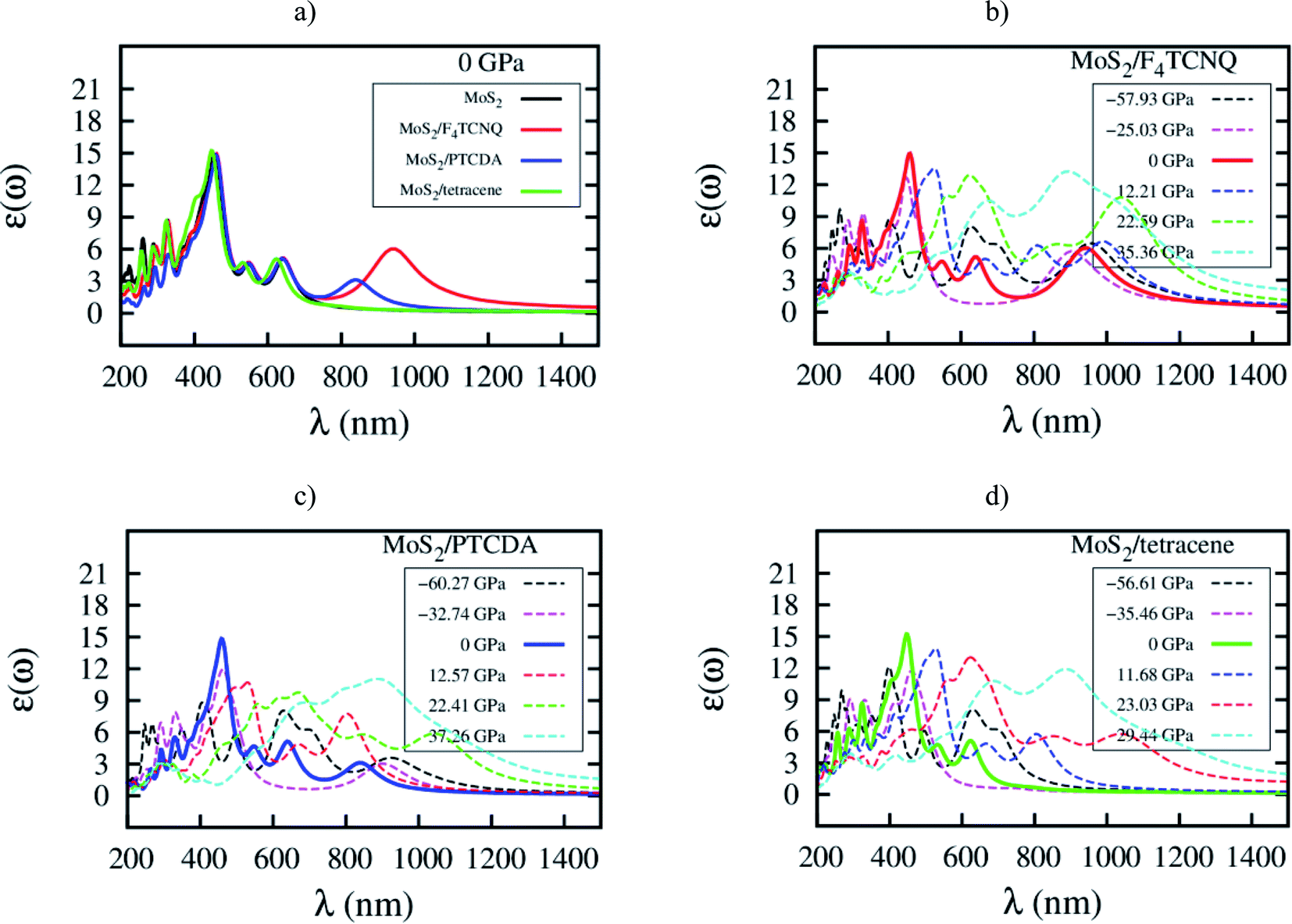
Here, we elucidate the influences of the organic molecular adsorption on the optical properties of the monolayer MoS2. The imaginary part of the frequency-dependent dielectric function of the MoS2, MoS2/F4TCNQ, MoS2/PTCDA, and MoS2/tetracene in the independent-particle approximation including local field effects is presented in Fig. 9. After that, optical parameters as listed in Table 6 can be obtained in two steps: (1) determining the wavelength λ and the intensity ε(ω) at the maximum peak of the dielectric function, check Fig. 9, (2) calculating the corresponding photon energy Ep = ℏc/λ. At zero pressure, we found in Fig. 9a that the optical spectrum of the MoS2/F4TCNQ, MoS2/PTCDA, and MoS2/tetracene systems has the maximum peak at almost the same position as that of the monolayer MoS2, which is at about 450 nm. The result indicates that these systems can emit and absorb blue light.29,37 The optical spectrum of the MoS2/tetracene has almost the same behavior as the monolayer MoS2 with a little modification at short wavelengths around 300 nm. Contrastingly, the MoS2/F4TCNQ and MoS2/PTCDA exhibits an additional peak at 950 and 850 nm, respectively. It is necessary to remind that the MoS2/F4TCNQ and MoS2/PTCDA are p-type, while the MoS2/tetracene is an n-type semiconductor. The behavior of the optical spectrum of the MoS2/tetracene was found to be similar to that of the n-type doping of MoS2 with PEI.33 Therefore, the auxiliary peak at a longer wavelength was only found for the monolayer MoS2 with the p-type doping.5 Furthermore, as shown in Fig. 9b–d, the intensity of the main optical peak at non-zero pressures was suppressed compared to that at 0 GPa.
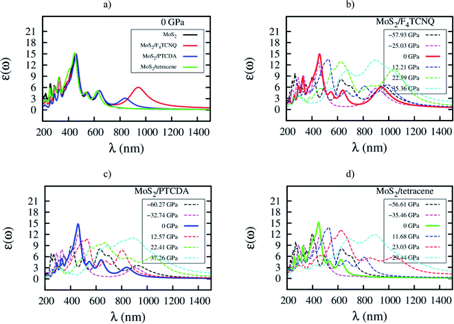 |
| | Fig. 9 Imaginary part of dielectric function ε(ω) versus wavelength λ for (a) the systems at zero pressure, (b) MoS2/F4TCNQ, (c) MoS2/PTCDA, and (d) MoS2/tetracene under pressure. | |
Table 6 The wavelength and dielectric function at the maximum intensity of optical spectrum
| Ep = hc/λ is the photon energy, λ is the photon wavelength, h is Planck constant, and c is the speed of light in vacuum. |
| MoS2 (ref. 33) |
P (GPa) |
−56.18 |
−32.44 |
0 |
10.13 |
24.95 |
41.14 |
| Ep (eV)a |
4.66 |
2.60 |
2.73 |
2.39 |
2.00 |
1.42 |
| λ (nm) |
266 |
477 |
453 |
521 |
621 |
873 |
| ε(ω) |
11.06 |
11.58 |
14.88 |
13.36 |
13.18 |
12.06 |
| MoS2/F4TCNQ |
P (GPa) |
−57.93 |
−25.03 |
0 |
12.21 |
22.59 |
35.36 |
| Ep (eV)a |
4.62 |
2.75 |
2.69 |
2.36 |
1.99 |
1.38 |
| λ (nm) |
268 |
451 |
461 |
526 |
624 |
896 |
| ε(ω) |
9.65 |
12.66 |
14.95 |
13.54 |
12.92 |
13.22 |
| MoS2/PTCDA |
P (GPa) |
−60.27 |
−32.74 |
0 |
12.57 |
22.41 |
37.26 |
| Ep (eV)a |
3.06 |
2.67 |
2.71 |
2.34 |
1.86 |
1.39 |
| λ (nm) |
405 |
463 |
458 |
529 |
668 |
889 |
| ε(ω) |
8.82 |
11.95 |
14.82 |
10.72 |
9.76 |
11.05 |
| MoS2/tetracene |
P (GPa) |
−56.61 |
−35.46 |
0 |
11.68 |
23.03 |
29.44 |
| Ep (eV)a |
3.11 |
2.69 |
2.77 |
2.36 |
1.99 |
1.40 |
| λ (nm) |
398 |
461 |
447 |
526 |
623 |
886 |
| ε(ω) |
12.11 |
11.72 |
15.21 |
13.85 |
13.03 |
11.90 |
4. Conclusion
This work investigated the effects of the organic molecular adsorption on the physical properties of the monolayer MoS2 by the DFT calculations. The results have proved that the adsorption of F4TCNQ, PTCDA, and tetracene on MoS2 is physisorption. The organic molecular adsorption reduces the direct bandgap of the monolayer MoS2 to 0.36, 1.43, and 0.72 eV, respectively. The main cause is due to the emergence of the new energy level at the conduction band minimum for MoS2/F4TCNQ and MoS2/PTCDA, and at the valence band maximum for MoS2/tetracene, by the pz orbitals of the adsorbates. Under pressure, the bandgap of the MoS2/F4TCNQ, MoS2/PTCDA, and MoS2/tetracene systems reaches the maximum value of 0.36, 1.43, and 0.87 eV, respectively. Whilst, it becomes 0 eV implying the transition to the metal at the tensile pressure of 22.59, 22.41, and 23.03 GPa in that order. The adsorption of tetracene changes the optical peak structure of the monolayer MoS2 at the ultraviolet region around 300 nm; however, the F4TCNQ and PTCDA adsorption generate an auxiliary peak at the long wavelengths.
Conflicts of interest
There are no conflicts of interest to declare.
Acknowledgements
This research is funded by Ho Chi Minh City University of Technology (HCMUT), VNU-HCM, under grant number BK-SDH-2021-1680479.
References
- B. Radisavljevic, A. Radenovic, J. Brivio, V. Giacometti and A. Kis, Single-layer MoS2 transistors, Nat. Nanotechnol., 2011, 6, 147–150 CrossRef CAS.
- A. Splendiani, L. Sun, Y. Zhang, T. Li, J. Kim, C.-Y. Chim, G. Galli and F. Wang, Emerging Photoluminescence in Monolayer MoS2, Nano Lett., 2010, 10, 1271 CrossRef CAS.
- K. F. Mak, C. Lee, J. Hone, J. Shan and T. F. Heinz, Atomically thin MoS2: a new direct-gap semiconductor, Phys. Rev. Lett., 2010, 105, 136805 CrossRef.
- M. Chhowalla, H. S. Shin, G. Eda, L.-J. Li, K. P. Loh and H. Zhang, The chemistry of two-dimensional layered transition metal dichalcogenide nanosheets, Nat. Chem., 2013, 5(4), 263–275 CrossRef.
- Y. Jing, X. Tan, Z. Zhou and P. Shen, Tuning electronic and optical properties of MoS2 monolayer via molecular charge transfer, J. Mater. Chem. A, 2014, 2, 16892–16897 RSC.
- W. Chen, S. Chen, D. C. Qi, X. Y. Gao and A. T. Wee, Surface transfer p-type doping of epitaxial graphene, J. Am. Chem. Soc., 2007, 129(34), 10418–10422 CrossRef CAS.
- Y. Du, H. Liu, A. T. Neal, M. Si and P. D. Ye, Molecular Doping of Multilayer MoS2 Field-Effect Transistors: Reduction in Sheet and Contact Resistances, IEEE Electron Device Lett., 2013, 0741–3106 Search PubMed.
- H. Huang, Y. Huang, S. Wang, M. Zhu, H. Xie, L. Zhang, X. Zheng, Q. Xie, D. Niu and Y. Gao, Van Der Waals Heterostructures between Small Organic Molecules and Layered Substrates, Crystals, 2016, 6, 113 CrossRef.
- Q. Huy Thi, H. Kim, J. Zhao and T. Hue Ly, Coating two-dimensional MoS2 with polymer creates a corrosive non-uniform interface, npj 2D Mater. Appl., 2018, 2, 34 CrossRef.
- H. Pinto, R. Jones, J. P. Goss and P. R. Briddon, p-type doping of graphene with F4TCNQ, J. Phys.: Condens. Matter, 2009, 21, 402001 CrossRef CAS.
- S. Mouri, Y. Miyauchi and K. Matsuda, Tunable Photoluminescence of Monolayer MoS2 via Chemical Doping, Nano Lett., 2013, 13(12), 5944–5948 CrossRef CAS.
- P. Hu, J. Ye, X. He, K. Du, K. K. Zhang, X. Wang, Q. Xiong, Z. Liu, H. Jiang and C. Kloc, Control of Radiative Exciton Recombination by Charge Transfer Induced Surface Dipoles in MoS2 and WS2 Monolayers, Sci. Rep., 2016, 6, 24105 CrossRef CAS.
- J. Wang, Z. Ji, G. Yang, X. Chuai, F. Liu, Z. Zhou, C. Lu, W. Wei, X. Shi, J. Niu, L. Wang, H. Wang, J. Chen, N. Lu, C. Jiang, L. Li and M. Liu, Charge Transfer within the F4TCNQ-MoS2 van der Waals Interface: Toward Electrical Properties Tuning and Gas Sensing Application, Adv. Funct. Mater., 2018, 28(51), 1806244 CrossRef.
- T. Ogawa, K. Kuwamoto, S. Isoda, T. Kobayashi and N. Karl, 3,4:9,10-Perylenetetracarboxylic dianhydride (PTCDA) by electron crystallography, Acta Crystallogr., Sect. B: Struct. Sci., 1999, 55, 123–130 CrossRef.
- S. Heutz, A. J. Ferguson, G. Rumbles and T. S. Jones, Morphology, structure and photophysics of thin films of perylene-3,4,9,10-tetracarboxylic dianhydride, Org. Electron., 2002, 3, 119–127 CrossRef CAS.
- Y. Han, W. Ning, H. Du, J. Yang, N. Wang, L. Cao, F. Li, F. Zhang, F. Xu and M. Tian, Preparation, Optical and Electrical Properties of PTCDA Nanostructures, Nanoscale, 2015, 7, 17116–17121 RSC.
- M. R. Habib, H. Li, Y. Kong, T. Liang, S. M. Obaidulla, S. Xie, S. Wang, X. Ma, H. Su and M. Xu, Tunable Photoluminescence in van der Waals Heterojunction Built from MoS2 Monolayer and PTCDA Organic Semiconductor, Nanoscale, 2018, 10, 16107–16115 RSC.
- S. Wang, C. Chen, Z. Yu, Y. He, X. Chen, Q. Wan, Y. Shi, D. W. Zhang, H. Zhou, X. Wang and P. Zhou, A MoS2/PTCDA Hybrid Heterojunction Synapse with Efficient Photoelectric Dual Modulation and Versatility, Adv. Mater., 2018, 31(3), 1806227 CrossRef.
- L. Daukiya, J. Seibel and S. D. Feyter, Chemical modification of 2D materials using molecules and assemblies of molecules, Adv. Phys., 2019, 4(1), 1625723 CAS.
- R. W. I. de Boer, T. M. Klapwijk and A. F. Morpurgo, Field-effect transistors on tetracene single crystals, Appl. Phys. Lett., 2003, 83, 4345 CrossRef CAS.
- H. J. Park, C.-J. Park, J. Y. Kim, M. S. Kim, J. Kim and J. Joo, Hybrid Characteristics of MoS2 Monolayer with Organic Semiconducting Tetracene and Application to Anti-Ambipolar Field Effect Transistor, ACS Appl. Mater. Interfaces, 2018, 10(38), 32556–32566 CrossRef CAS.
- G. Kresse and J. Hafner, Ab initio molecular dynamics for open-shell transition metals, Phys. Rev. B: Condens. Matter Mater. Phys., 1993, 48, 13115–13118 CrossRef CAS.
- G. Kresse and J. Hafner, Ab initio molecular-dynamics simulation of the liquid-metal–amorphous-semiconductor transition in germanium, Phys. Rev. B: Condens. Matter Mater. Phys., 1994, 49, 14251–14269 CrossRef CAS.
- G. Kresse and J. Furthmuller, Efficient iterative schemes for ab initio total-energy calculations using a plane-wave basis set, Phys. Rev. B: Condens. Matter Mater. Phys., 1996, 54, 11169–11186 CrossRef CAS.
- P. E. Blochl, Projector augmented-wave method, Phys. Rev. B: Condens. Matter Mater. Phys., 1994, 50, 17953 CrossRef.
- G. Kresse and J. Joubert, From ultrasoft pseudopotentials to the projector augmented-wave method, Phys. Rev. B: Condens. Matter Mater. Phys., 1999, 59, 1758 CrossRef CAS.
- J. P. Perdew, J. A. Chevary, S. H. Vosko, K. A. Jackson, M. R. Pederson, D. J. Singh and C. Fiolhais, Atoms, molecules, solids, and surfaces: applications of the generalized gradient approximation for exchange and correlation, Phys. Rev. B: Condens. Matter Mater. Phys., 1992, 46, 6671 CrossRef CAS.
- J. P. Perdew, K. Burke and M. Ernzerhof, Generalized Gradient Approximation Made Simple, Phys. Rev. Lett., 1996, 77, 3865 CrossRef CAS.
- Y. Li, Y.-L. Li, C. M. Araujo, W. Luo and R. Ahuja, Single-layer MoS2 as an efficient photocatalyst, Catal.: Sci. Technol., 2013, 3, 2214 RSC.
- H. J. Monkhorst and J. D. Pack, Special points for Brillouin zone integrations, Phys. Rev. B: Solid State, 1976, 13, 5188–5192 CrossRef.
- J. Shang, L. Zhang, X. Cheng and F. Zhai, Pressure induced effects on the electronic and optical properties of MoS2, Solid State Commun., 2015, 219, 33–38 CrossRef CAS.
- L. J. Kong, G. H. Liu and L. Qiang, Electronic and optical properties of O-doped monolayer MoS2, Comput. Mater. Sci., 2016, 111, 416–423 CrossRef CAS.
- O. K. Le, V. Chihaia, M.-P. Pham-Ho and D. N. Son, Electronic and optical properties of monolayer MoS2 under the influence of polyethyleneimine adsorption and pressure, RSC Adv., 2020, 10, 4201–4210 RSC.
- M. M. Ugeda and A. J. Bradley, et al., Giant bandgap renormalization and excitonic effects in a monolayer transition metal dichalcogenide semiconductor, Nat. Mater., 2014, 13, 1091–1095 CrossRef CAS.
- X. Cheng, Y. Li, J. Shang, C. Hu, Y. Ren, M. Liu and Z. Qi, Thickness-dependent phase transition and optical behavior of MoS2 films under high pressure, Nano Res., 2018, 11, 855–863 CrossRef CAS.
- V. K. Dien, O. K. Le, V. Chihaia, M. P. Pham-Ho and D. N. Son, Monolayer transition-metal dichalcogenides with polyethyleneimine adsorption, J. Comput. Electron., 2021 DOI:10.1007/s10825-020-01630-2.
- Z. Yin, H. Li, H. Li, L. Jiang, Y. Shi, Y. Sun, G. Lu, Q. Zhang, X. Chen and H. Zhang, Single-Layer MoS2 Phototransistors, ACS Nano, 2011, 6, 74–80 CrossRef.
Footnote |
| † Electronic supplementary information (ESI) available. See DOI: 10.1039/d0ra10075g |
|
| This journal is © The Royal Society of Chemistry 2021 |
Click here to see how this site uses Cookies. View our privacy policy here. 
 Open Access Article
 This Open Access Article is licensed under a Creative Commons Attribution-Non Commercial 3.0 Unported Licence
 c,
Vo Van Ond and
Do Ngoc Son
c,
Vo Van Ond and
Do Ngoc Son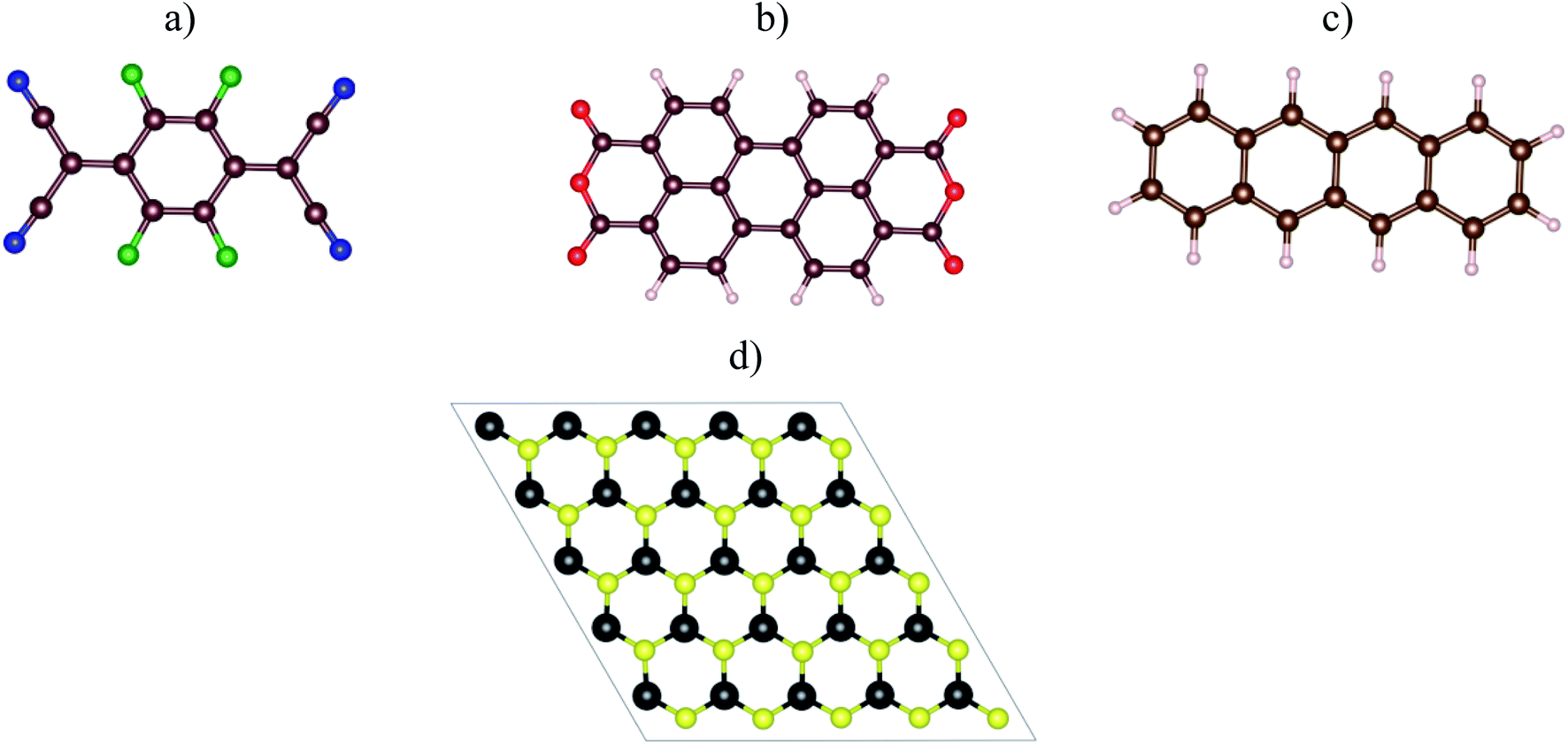
 (a is the lattice constant and c is the thickness of the slab). The pressure is modified by changing the lattice constant a = b.