
 Open Access Article
 This Open Access Article is licensed under a Creative Commons Attribution-Non Commercial 3.0 Unported Licence
Influence of molybdenum and technetium doping on visible light absorption, optical and electronic properties of lead-free perovskite CsSnBr3 for optoelectronic applications
M. I. Kholil *,
M. T. H. Bhuiyan*,
M. Atikur Rahman,
M. S. Ali and
M. Aftabuzzaman*
*,
M. T. H. Bhuiyan*,
M. Atikur Rahman,
M. S. Ali and
M. Aftabuzzaman*
Department of Physics, Pabna University of Science and Technology, Pabna, 6600, Bangladesh. E-mail: ibrahim.physics20@gmail.com; thbapon@pust.ac.bd; azamanphy@pust.ac.bd
First published on 12th January 2021
Abstract
Lead-free metal halide perovskites have nowadays become familiar owing to their potential use in solar cells and other optoelectronic applications. In this study, we carried out the structural, elastic, electronic, and optical properties of pure and metal (Mo/Tc) doped CsSnBr3 by using the density functional theory. The metal doping CsSnBr3 displays a narrowing band gap and as a result the optical functions exhibit high absorption and high conductivity in the visible region. Metal doping samples also reveal a high dielectric constant which indicates a low charge-carrier recombination rate and hence enhances the device performance. The optical absorption spectra of metal doped samples greatly shifted (red-shift) towards the lower energy region compared with the pure sample which creates a high-intensity peak in the visible region. The mechanical parameter reveals a highly ductile, soft, and flexible nature which indicates the suitability for use in thin films. The electronic band structure of metal-doped CsSnBr3 shows an intermediate state that assists the excited electron to pass on from valence band to conduction band. The overall study suggests that lead-free CsSn0.875Tc0.125Br3 perovskite is a promising candidate for solar cells and other optoelectronic applications.
1. Introduction
Metal halide perovskites are widely used nowadays due to their diverse optoelectronic properties such as tunable band gap nature, high absorption coefficient and conductivity, low reflectivity, extended charge diffusion length, large charge carrier mobility, lower carrier recombination rate, and low excitation binding energy.1,2 These extraordinary properties make perovskite materials suitable to use in solar cells and other optoelectronic properties. Consequently, in recent years, researchers have been greatly interested in these perovskite materials to conduct their research. Metal halide perovskites are also used in the extended area of the electronic field including light-emitting diodes (LEDs), photovoltaics, and solar-to-fuel energy conversion devices.3–6 Semiconducting metal halide perovskites consist of ABX3 formula, where A represents the positive ion, B is a metal ion and X denotes the halogen anion. These semiconducting perovskite materials are inexpensive and abundantly available on earth, which is one of the main reasons for the giant interest of the scientific community. On the other hand, abundance and cost effectiveness make perovskite materials more efficient and economical to use in solar cells and other optoelectronic applications than current silicon-based photovoltaic (PV) technology.1Lead halide perovskites already attack immense interest due to their excellent feature including power-conversion efficiencies as well as simple and cheap processability.7 Although the material meets the necessary condition to use in optoelectronic technology but the major concern comes up owing to their presence of toxicity of Pb and hence they are not environmentally friendly. As for example, lead-based PbI2 perovskite is poisonous according to environmental conditions.8–10 On the other hand, the feature of device instability and J–V hysteresis are the key defects of Pb contain perovskite materials.11 To overcome the toxicity, recently researchers have been executed some theoretical and experimental work by substituting favorable metal cation.12,13
Optical properties predicted by Roknuzzaman et al.12 reveal that CsSnBr3 perovskites possess a medium absorption coefficient and less optical conductivity in the visible region. Therefore, CsSnBr3 is not suitable to use in a solar cell and other optoelectronic applications. Although this material shows ductile in nature, but it has a wider experimental band gap 1.75 eV.14 An appropriate metal doping can reduce the band gap and hence increase the possibility to enhance the absorptive nature as well as conductivity in the visible region. Consequently, here we consider the metal doping in the Sn site of CsSnBr3 to find out the enhanced optical nature in the visible region. M. G. Brik15 suggested the narrowing band gap of CsSnBr3 but the Poisson's ratio (0.0809) reveals the brittle nature of this material. He also studied CsCaBr3 and CsGeBr3 perovskites but these also reveal the brittle nature. Therefore, the studied materials may not be acceptable to use in some high ductility required applications and hence high ductility is demanded as a promising material.16 In addition, Mahmood et al.17 proposed the ductile nature (Pugh's ratio 2.39) of CsSnBr3 and high absorption but the material shows a large band gap (1.72 eV) as experimental value (1.75 eV). The investigation of metal-doped CsGeCl3 available in the literature18 reveals that Poisson's ratio (0.26) stays in a critical position and hence separation is needed to consider ductile/brittle nature. Consequently, CsGeCl3 is not acceptable as promising for optoelectronic applications. The metal-doped CsGeCl3 and CsSnCl3 show high absorption and conductivity but the reflectivity is also high enough in the visible region.16,18 As a result, these metal doping is not considered as a highly absorbing material and hence not suitable to use in solar cells and other optoelectronic applications. Supercell symmetry is highly required for doped samples to search for the appropriate physical properties;19 however, supercell symmetry is absent in metal doped CsGeCl3 and CsSnCl3.16,18 Another Ni-doped of CsGeBr3 investigation7 suggests the enhanced absorption in the visible and ultraviolet region but it is not considered as high absorption than the pristine one. On the other hand, pristine CsGeI3 shows high optical absorption but it reveals brittle in nature12 and hence not advantageous to use in practical applications. Therefore, in our present investigation, the structural, elastic, electronic, and optical properties of Mo- and Tc-doped CsSnBr3 have been calculated to find out the promising solar cell material with outstanding optoelectronic properties by using density functional theory (DFT). Finally, the present results of the metal-doped sample compared with the pristine and other well-known perovskite material to reveal the enhanced results of key properties.
2. Computational methods
The present ab initio investigation was carried out by using density functional theory (DFT)20,21 within the Cambridge Serial Total Energy Package (CASTEP) computer program.22 The geometry optimization was performed by using the generalized gradient approximation (GGA) within the Perdew–Burke–Ernzerhof (PBE) functional for exchange–correlation interactions.23 The ultrasoft pseudopotentials were used as a Vanderbilt type to describe the electron ions interactions.24 The plane-wave cutoff energy was set to 600 eV for pure CsSnBr3 and 350 was used for metal (Mo and Tc) doped CsSnBr3 to execute the investigation. Monkhorst–Pack technique was used to generate the k-point in the first Brillouin zone.25 The k-points grid was used to 14 × 14 × 14 and 3 × 3 × 3 for pure and doped samples, respectively for obtaining the better convergence. The Broyden–Fletcher–Goldfarb–Shanno (BFGS) technique was employed to ensure the minimization of total energy, internal forces, and external stresses.26 Finite-strain theory27 was employed to calculate the elastic constants Cij and the theory was involved in a set of homogeneous strains to relax the atomic degrees of freedoms. The set of homogeneous strains employed in a unit cell was involved in six-stress components σij for each strain δj. A scissor value was set to 1.1961 eV in the time of analysis of optical functions to minimize the band gap within the theoretical (0.5539 eV) and experimental (1.75 eV). The formulas of optical properties that support the CASTEP to evaluate the optical functions are available in the literature.283. Results and discussion
3.1. Structural properties
The semiconducting lead-free perovskite CsSnBr3 crystallizes with a cubic structure in the space group Pm![[3 with combining macron]](https://www.rsc.org/images/entities/char_0033_0304.gif) m (No. 221).12 The cubic unit cell contains five atoms (3 Br, 1 Sn and 1 Cs). The coordinates of Cs atoms are (0, 0, 0) situated in the corner of the unit cell with Wyckoff position 1a, Sn atom is located in the body-center position with Wyckoff site 1b and Br atoms are situated in the face-center position with Wyckoff position 3c.12 Here, we constructed the 2 × 2 × 2 supercell of the unit cell of CsSnBr3 to dope the suitable metal. As a result, the supercell increases the atomic number eight times than the pure unit cell. Then, the total atomic number 40 (24 Br, 8 Sn and 8 Cs) was found in the supercell as shown in Fig. 1. Here, we replaced the one Sn atom in the supercell with appropriate metal (Mo & Tc) doping and hence the doping concentration 12.5% was raised. The doping formula is considered here CsSn0.875Mo0.125Br3 or CsSn0.875Tc0.125Br3. The calculated lattice constants a, and unit cell volume V are recorded in Table 1. The obtained results of lattice parameters and volume are in good agreement with available experimental14,29 and theoretical12,15 results. It is observed from Table 1 that the lattice constant and volume are decreased after metal doping due to the lower ionic radii of dopants Mo4+ (0.650 Å) and Tc4+ (0.645 Å) than the pristine element Sn4+ (0.690 Å).30
m (No. 221).12 The cubic unit cell contains five atoms (3 Br, 1 Sn and 1 Cs). The coordinates of Cs atoms are (0, 0, 0) situated in the corner of the unit cell with Wyckoff position 1a, Sn atom is located in the body-center position with Wyckoff site 1b and Br atoms are situated in the face-center position with Wyckoff position 3c.12 Here, we constructed the 2 × 2 × 2 supercell of the unit cell of CsSnBr3 to dope the suitable metal. As a result, the supercell increases the atomic number eight times than the pure unit cell. Then, the total atomic number 40 (24 Br, 8 Sn and 8 Cs) was found in the supercell as shown in Fig. 1. Here, we replaced the one Sn atom in the supercell with appropriate metal (Mo & Tc) doping and hence the doping concentration 12.5% was raised. The doping formula is considered here CsSn0.875Mo0.125Br3 or CsSn0.875Tc0.125Br3. The calculated lattice constants a, and unit cell volume V are recorded in Table 1. The obtained results of lattice parameters and volume are in good agreement with available experimental14,29 and theoretical12,15 results. It is observed from Table 1 that the lattice constant and volume are decreased after metal doping due to the lower ionic radii of dopants Mo4+ (0.650 Å) and Tc4+ (0.645 Å) than the pristine element Sn4+ (0.690 Å).30
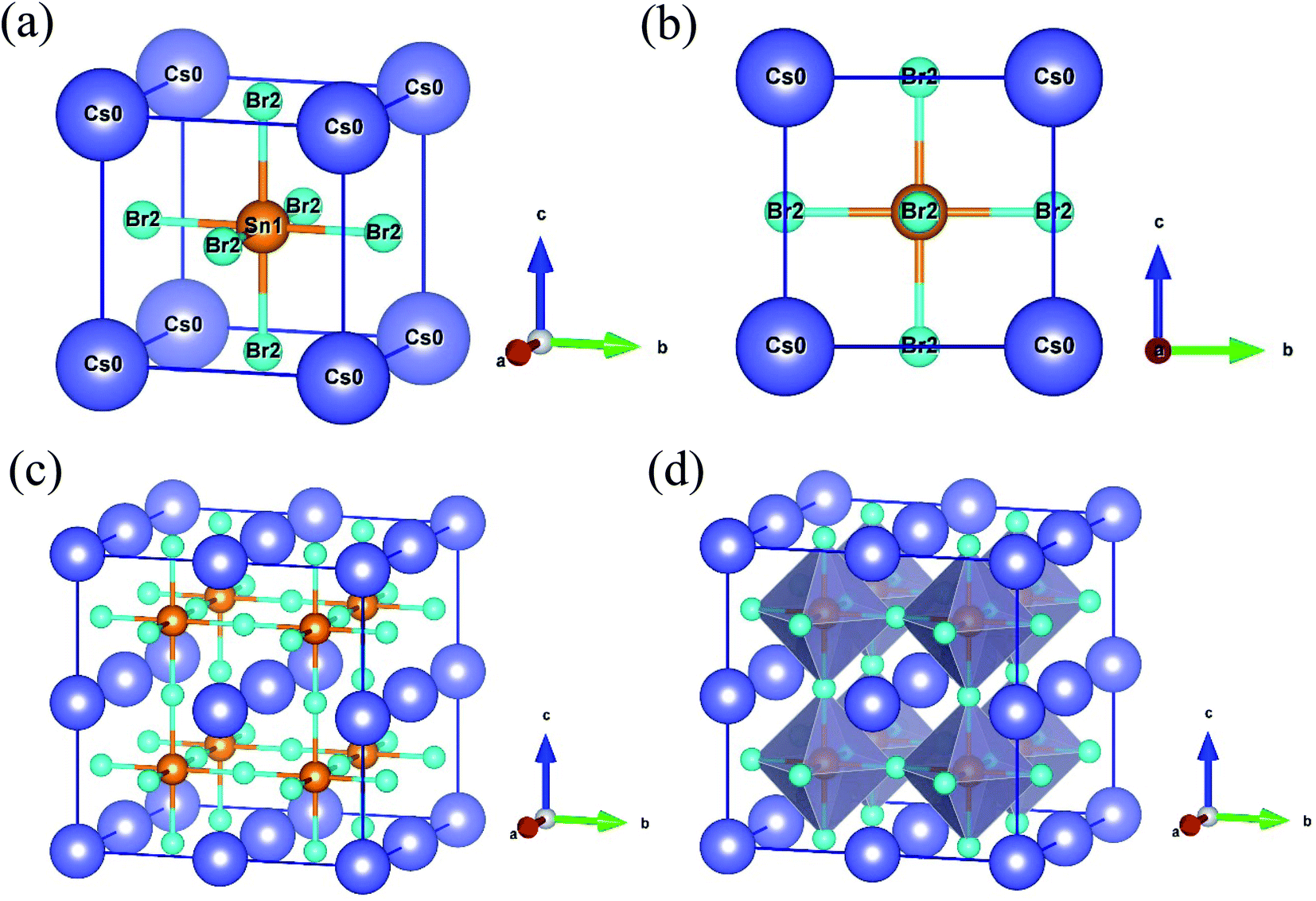 | ||
| Fig. 1 Crystal structure of CsSnBr3: (a) unit cell, (b) 2D view of unit cell in bc plane, (c) constructed 2 × 2 × 2 supercell, and (d) polyhedral form of supercell. | ||
3.2. Optical properties
Optical properties are the most essential parameter to justify the suitability of a material for solar cells and other optoelectronic devices. The details optical properties such as absorption coefficient, conductivity, reflectivity, and dielectric constant are calculated and discussed here up to 20 eV of intrinsic and doped samples to understanding the behavior in visible light and high photon energy radiation. According to a literature, CsSnBr3 perovskite possesses medium absorption and less conductivity under visible light range.12 Therefore, these optical behaviors are not considered reasonable in solar cell and optoelectronic applications. In the present investigation, metal doping is considered to enhance the optical nature in the visible energy range and significantly improve the performance of device applications.The optical absorption coefficient defined the material ability to measure the penetration of light when a certain wavelength of light or energy is incident on the material surface and it penetrated until it is fully absorbed by the material.31 It is extremely significant to reveal absorption behavior as well as solar energy conversation capability. The investigated absorption coefficient of pure form and metal (Mo, Tc) doped samples are displayed in Fig. 2 as a function of photon energy and wavelength of light. The calculated absorption spectra as a function of photon energy, as shown in Fig. 2(a), represent that the absorption spectra of metal doping samples largely shifted (red-shift) towards the low photon energy region as compare to pure form. The metal doping enhances the absorption coefficient between 1.0 eV to 9.0 eV region. It is also observed that two additional peaks occurred at 2 eV (low) and 6.5 eV (high). Therefore, the enhanced absorption in visible as well as some part of the high-energy region explicitly represents the higher ability of absorption under metal doping. The Tc-doped sample with compare to Mo-doped exhibits the greater absorption quality and the reason for this difference is clearly explained in the electronic properties section.
 | ||
| Fig. 2 Calculated absorption coefficient as a function of (a) photon energy and (b) wavelength of light of pure and doped form of CsSnBr3. | ||
Fig. 2(b) represents the absorption coefficient as a function of the wavelength of light and this was mainly calculated to elucidate the absorption behavior in the visible energy region. As compared to pure form, the metal-doped sample enhances the absorption largely entire the visible energy region. The Tc-doped sample is better enhanced the absorption spectra in the visible region than the Mo-doped sample. On the other hand, the pure form shows negligible absorption spectra in the visible region as compared to the doped form. In general, the wider band gap semiconducting material has the ability to use 4% of ultraviolet light of solar spectrum and on the contrary, the material used visible light 44% of the solar spectrum.32,33 Therefore, the pure form of CsSnBr3 with a large experimental band gap (1.75) is not suitable to proper utilization of the visible light absorption and hence the performance is not considered significant in solar cells and other optoelectronic applications. The Tc-doped CsSnBr3 represents the large absorption compared to Mo-doped and pure form of CsSnBr3. Consequently, the Tc-doped sample reveals the greater ability to utilize the visible light of the solar spectrum and may use to increase the performance of solar cell devices.
The real part of conductivity spectra as a function of photon energy is calculated here up to 12 eV and displayed in Fig. 3(a). Optical conductivity mainly reveals the reflection of photoconductivity.34 Consequently, photoconductivity as well as electrical conductivity is increased due to the absorption of light energy. Conductivity in low energy (visible) range of metal-doped sample has shown higher compare to pure sample. An additional peak of Mo- and Tc-doped CsSnBr3 is also observed in the low energy region, but for pure CsSnBr3 conductivity is negligible between 0 and 2.25 eV. Although pure samples conductivity reveals high in higher energy region than doped samples, but here we mainly focus on the effect of metal doping in the visible region. Therefore, the Tc-doped sample revealed a higher conductivity in the lower energy region as well as a visible region than the Mo-doped and pure form of CsSnBr3. The high conductivity in Tc-doped samples is observed in the visible region due to higher absorption (Fig. 2) in that region. Hence, the Tc-doped sample is suitable to use in solar cells and other optoelectronic applications.
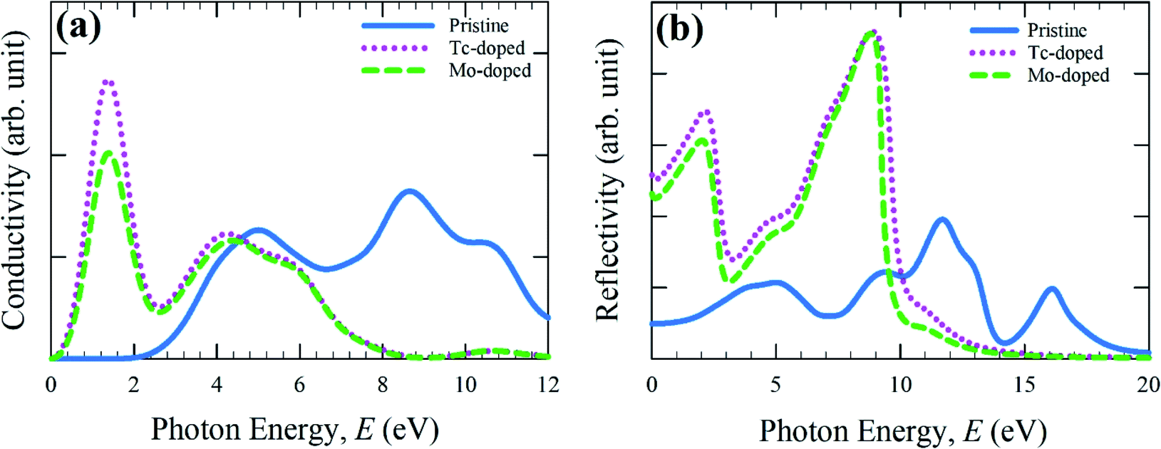 | ||
| Fig. 3 Calculated (a) conductivity and (b) reflectivity spectra as a function of photon energy. | ||
The optical reflectivity of a material determines the materials ability to reflect the incident light on the material surface. It is one of the essential properties of a material to find out the suitability to use in optoelectronic applications. The optical reflectivity spectra are calculated here up to 20 eV and illustrated in Fig. 3(b). It is evident from Fig. 3(b) that the reflectivity of metal-doped samples is higher compared to the pristine sample up to 10 eV, but in higher energy, it displayed lower reflectivity. The reflectivity of metal-doped samples in the visible region is decreased and exhibited two peaks in around 2.0 eV and 8.5 eV. The Tc-doped samples show higher conductivity than the Mo-doped sample. However, the present Tc-doped and Mo-doped samples show lower reflectivity compared to metal-doped in CsSnCl3 and CsGeCl3.16,18 Therefore, more investigation is required to reduce the conductivity in the visible region as well as the low energy region, which may enhance the absorption and conductivity in the visible region as well as device performances.
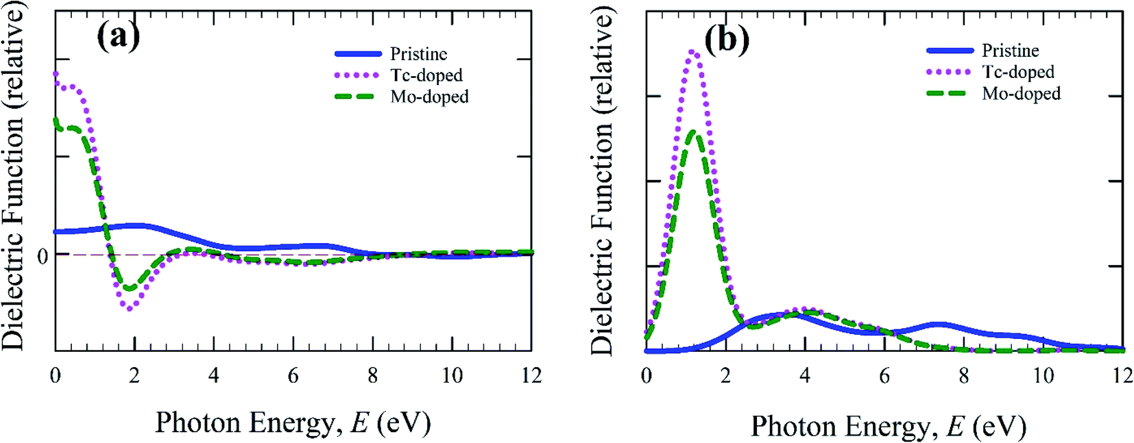
The calculated real and imaginary part of dielectric function is shown in Fig. 4 and calculation was carried out up to 12 eV. Dielectric function is responsible for charge-carrier recombination rate.35 The static value of real part of the dielectric function reveals this recombination. The greater static value reduces the charge-carrier recombination and hence increases the efficiency of optoelectronic applications. The static value of the real part of the doped samples is higher than the pristine samples. An additional peak is also observed in the low energy region as shown in Fig. 4(b). The pure form sample shows a negligible effect compared to doped samples. Material with a large band gap reveals the lower dielectric value.36 In the present calculation, the metal-doped samples reduce the band gap (Fig. 5), and hence Tc- and Mo-doped CsSnBr3 show higher dielectric value. The imaginary part mainly responsible for the electronic band structure of a material and reveal the absorption nature.37 The imaginary part of the dielectric function, as shown in Fig. 4(b), exhibited a large peak in the low energy region for metal-doped samples, which increased the absorption (Fig. 2) in low energy region. The Tc-doped sample shows a higher dielectric constant value than Mo-doped and pure form of metal CsSnBr3. Therefore, Tc-doped CsSnBr3 could reveal better performance in optoelectronic applications. The real and imaginary part of the dielectric function shows a negligible effect around 9 eV and 10 eV for the metal-doped and pure form of CsSnBr3. Hence, the investigated samples revealed the high transparency in the higher energy region (above 8 eV) and as a result, it shows low absorption in the higher energy region.
 | ||
| Fig. 4 Calculated (a) real part, and (b) imaginary part of dielectric function as a function of photon energy. | ||
 | ||
| Fig. 5 Calculated electronic band structure of (a) pure unit cell, (b) pure 2 × 2 × 2 supercell, (c) Mo-doped and (d) Tc-doped of CsSnBr3 perovskites. | ||
3.3. Electronic properties
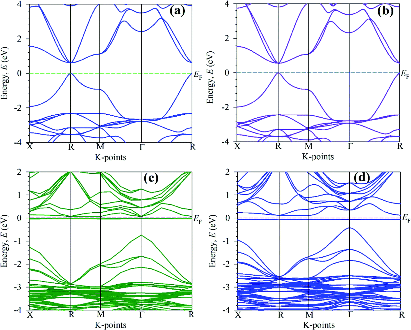
The electronic band structure is calculated here to understanding the electronic properties of pure and metal-doped CsSnBr3. The calculation of band structure is also crucial for observation of optical function. The band structure is calculated here are represented in Fig. 5. The horizontal dotted line at 0 eV considers the Fermi level. In general, the semi-conductive theory reveals the importance of material around the Fermi level and signifies the physical performance of a material. Therefore, here, we mainly focus on the conduction band (CB) and valence band (VB) behavior near the Fermi level to analyze the material characteristics. Fig. 5(a) represents the band structure of a unit cell of the pure form of CsSnBr3. It is manifest from Fig. 5(a) that the VB maximum and CB minimum occur at the same k-point, R. Therefore, the pure form of the unit cell represents the direct band gap nature. The observed band gap in R k-point is 0.614 eV, which is good agreement with the published band gap calculated by Roknuzzaman et al.12 and Körbel et al.,38 as shown in Table 2.The calculated electronic band structure of pure supercell is displayed in Fig. 5(b). The observed band gap is 0.5539 eV at R k-points and reveals the direct band gap nature as the pristine unit cell. There is some variation of band gap observed between the pure unit cell and pure supercell due to eight times unit cell consideration in the supercell. The experimental band gap 1.75 eV (ref. 14) of CsSnBr3 highly contradicts with observed band gap of pure unit cell and pure supercell of CsSnBr3. Therefore, it is clear that the present GGA calculation underestimates the experimentally observed value of band gap. This underestimation is the general limitation of the GGA approach owing to correlation effects and electron–electron exchange approximation.16 The band gap is also underestimating in LDA functional and LDA+U techniques based calculation. For that case, the researcher developed few techniques that reduce the usual problem of underestimation including hybrid functional39 and GW method,40 however, these techniques reveal some great limitations. On the other hand, GGA+U41 functional-based calculation overcome the partial underestimation between theoretical and experimental band gap. However, here we focus on the comparative evaluation of band structure and DOS of pure and metal-doped CsSnBr3 that are not influenced by the GGA approach.
The calculated electronic band structure of Mo-doped CsSnBr3 is displayed in Fig. 5(c). The valence band maximum and conduction band minimum in Fig. 5(c) occurs at two different k-points (Γ and R) that indicate the indirect band gap nature of Mo-doped samples. The observed band gap is 0.806 eV between these two k-points. An intermediate state is observed in the band gap. Although the calculated band gap of Mo-doped material is large compared to pristine material but the optical nature is more significant than the pristine sample due to the creation of an intermediate state inside the band gap. The intermediate state mainly arises due to the metal doping effect and this helps the excited electron in the valence band to pass the conduction band easiest way. The observed indirect band gap between the intermediate state and conduction band is 0.081 eV. The calculated electronic band structure of the Tc-doped CsSnBr3 is illustrated in Fig. 5(d). The observed band gap is 0.540 eV in two different k-points that indicates the indirect band gap nature of Tc-doped sample. An intermediates state in the band gap is also observed here. The narrowing band gap as well as the presence of an intermediate state make the transfer of excited electron in VB to CB easier than the Mo-doped and pure samples. The band gap of the intermediate state and conduction band is 0.179 eV that also indicates the indirect band gap nature.
It is obvious from Fig. 5(c) and (d) that the Fermi level shifted towards the conduction band compared to the pristine samples. This was happened due to metal doping. With compared to metal-doped and pure sample, it is clear that Tc-doped material possesses a greater absorption as well as conductivity in the visible region due to the narrowing band gap. Therefore, Tc-doped sample is more significant to use in a solar cell and other optoelectronic applications. Fig. 6 represent schematic diagram of energy band and bar charts of the observed band gap of pure and metal-doped CsSnBr3 with available experimental and theoretical results.
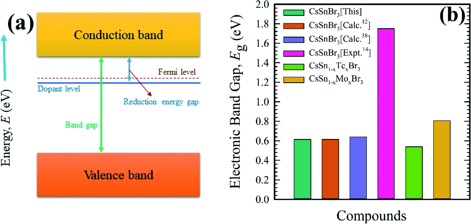 | ||
| Fig. 6 Schematic diagram of energy band (a), and bar charts (b) of electronic band gap (Eg) of pure and metal (Mo/Tc)-doped CsSnBr3. | ||
The calculated total and partial density of states of pure form and metal-doped form are represented in Fig. 7. The density of states of a pure supercell in Fig. 7(a) represented that the TDOS mainly arises with strong contribution of Br-4p, Br-4s, and Cs-5p states in the whole energy range. The valence band contribution arises here due to the large contribution of Br-4p and Sn-5p with a small admixture of Sn-5s, Cs-6s, and Cs-5p states. On the other hand, the TDOS above the Fermi level (conduction band) mostly originates from the Br-4p and Cs-5p with some admixture of Sn-5p, Sn-5s, Br-4s, and Cs-6s states.
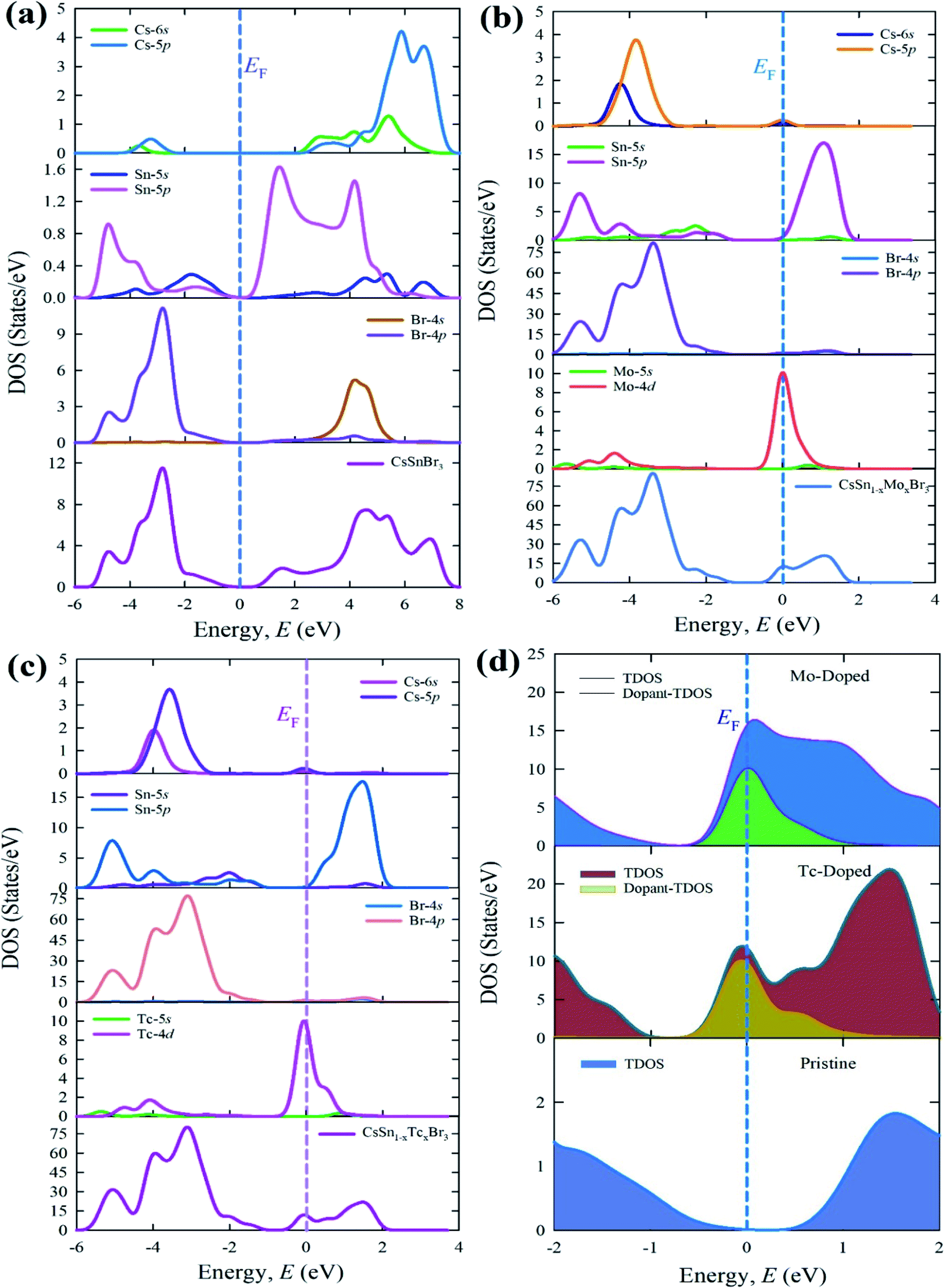 | ||
| Fig. 7 Calculated total and partial density of states (a) pure supercell (b) Mo-doped, (c) Tc-doped, and (d) dopant contribution near the Fermi level of CsSnBr3. | ||
The TDOS and PDOS of metal (Mo and Tc) doped materials are displaced in Fig. 7(b) and (c). The overall DOS of the Mo-doped and Tc-doped samples reveal similar contribution in the whole energy range. The DOS of Mo- and Tc-doped samples mainly arises due to the strong contribution of Br-4p states in the valence band whereas Sn-5p contributed to the conduction band. The dopant atom contributed to the Fermi level by the contribution of Mo-4d and Tc-4d states. The DOS show in the Fermi level due to the dopant level creation near the Fermi level. This dopant level responsible to increase the conduction electron and hence enhances the absorption in the visible region. The doped form of CsSnBr3 with compared to pure CsSnBr3 shows that the Femi level shifted along with the conduction band due to the metal doping effect.
The TDOS of dopant atom is presented here in Fig. 7(d) to understand the contribution in the Fermi level. This TDOS of the dopant atom is responsible to make the intermediate level close to the Fermi level. The intermediate level reduces the difference of band gap and significantly transfer the excited electron from VB to the intermediate state and then to CB under visible light absorption. Therefore, the red-shift of absorption spectra and the high peaks are observed in the visible region.
3.4. Mechanical properties
The single elastic constants of pure CsSnBr3 and metal-doped CsSnBr3 calculated here to understand the mechanical stability. Here, we used finite strain theory27 in a CASTEP modulus to calculate the three independent elastic constants for a cubic crystal such as C11, C12, and C44. The investigated results of the elastic constant are recorded in Table 3 and it is evident that these values good agreement with available theoretical values.12 The pure and metal-doped CsSnBr3 samples should satisfy the following Born stability criteria:42 C11 + 2C12 > 0, C44 > 0, and C11–C44 > 0. The recorded results of a single elastic constant obey these criteria, which indicate the mechanical stability of all samples. The Cauchy pressure is defined as (C12–C44),43 which reveals the ductile and brittle nature based on its positive and negative value. The calculated pure and metal-doped samples show positive Cauchy pressure, which confirms the ductile nature.| Phase | C11 | C12 | C44 | C12–C44 | Ref. |
|---|---|---|---|---|---|
| CsSnBr3 | 45.36 | 7.42 | 5.59 | 1.83 | This work |
| 43.89 | 6.69 | 5.21 | 1.48 | Calc.12 | |
| CsSn1−xMoxBr3 | 43.07 | 9.08 | 5.37 | 3.71 | This work |
| CsSn1−xTcxBr3 | 45.16 | 8.03 | 5.69 | 2.34 | This work |
The polycrystalline elastic modulus such as bulk modulus, Shear modulus, Young's modulus, Pugh's ratio, and Poisson's ratio of pure and metal-doped CsSnBr3 are calculated by using the equation available in the literature44 and recorded in Table 4. The studied results are in good agreement with available theoretical results.12 The calculated bulk modulus of metal-doped materials reveals the low enough as pristine samples and indicates the soft and flexible nature. Therefore, the metal-doped and pure samples are suitable to make the thin film as well as promising to use more functional in solar cells and other optoelectronic applications. A similar nature is also observed for Shear and Young's modulus. Fig. 8 represent the variation of single (C11, C12, and C44) and polycrystalline elastic modulus (B, G, and E) of pure and metal (Tc/Mo) doped samples.
| Phase | B (GPa) | G (GPa) | E (GPa) | B/G | v | Ref. |
|---|---|---|---|---|---|---|
| CsSnBr3 | 20.07 | 9.37 | 24.32 | 2.141 | 0.298 | This work |
| 19.09 | 8.94 | 23.19 | 2.135 | 0.30 | Calc.12 | |
| CsSn1−xMoxBr3 | 20.42 | 8.71 | 22.87 | 2.344 | 0.313 | This work |
| CsSn1−xTcxBr3 | 20.41 | 9.36 | 24.36 | 2.181 | 0.301 | This work |
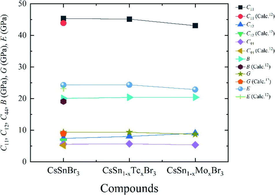 | ||
| Fig. 8 Variation of single (C11, C12, and C44) and polycrystalline elastic modulus (B, G, and E) of pure and metal-doped samples with x = 0.125. | ||
Pugh's ratio (B/G) and Poisson's ratio define the failure mode such as the ductile-brittle nature of a material.45–47 The critical value to separate the failure mode for Pugh's ratio is 1.75 and for Poisson's ratio is 0.26. The higher value of a material than the critical one denotes the ductile nature; otherwise, the material represents the brittle nature. The obtained value of pure and metal-doped samples represents the highly ductile nature according to the criteria. Therefore, the metal-doped samples are promising to use in optoelectronic applications. Fig. 9 represents the variation of Pugh's ratio and Poisson's ratio of pure and metal-doped CsSnBr3.
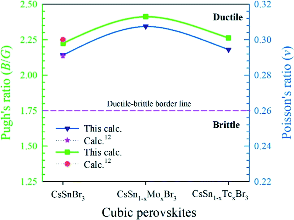 | ||
| Fig. 9 Variation of Pugh's ratio and Poisson's ratio of pure and metal-doped CsSnBr3 with (x = 0.125). | ||
3.5. Lead-free perovskites
The optical properties reported in the literature12 suggest that lead-free CsGeI3 is suitable to use in optoelectronic applications due to its high absorption and high conductivity, but the material show brittle in nature. As a result, the material may not consider appropriate in all practical applications. However, metal-doped CsGeBr3 reported in a theoretical investigation7 suggest the ductile in nature, but the absorption and conductivity are not good enough compared to the pristine sample. On the other hand, metal-doped CsSnCl3 and CsGeCl3 executed in a literature16,18 point out the highly ductile, high absorption and high conductivity in nature but these samples show high reflectivity than CsGeBr3. The pristine sample CsSnBr3 investigated by Roknuzzaman et al.12 suggests medium absorption and less conductivity. The lead-free CsSnBr3 also exhibits large experimental band gap 1.75.14 Consequently, the pristine CsSnBr3 perovskite is not suitable to use in solar cells and optoelectronic applications. Here, we studied the metal doping CsSnBr3 to enhance the optoelectronic properties. The metal doping CsSnBr3 mechanical properties reveal the highly ductile nature as well as the lower value of bulk modulus. Consequently, metal doping CsSnBr3 is promising to make thin films. The optical properties of Mo- and Tc-doped samples reveal the high absorption and high conductivity in the visible region. Although reflectivity in metal-doped CsSnBr3 is high in IR, visible and few parts of UV region than pristine CsSnBr3 but in visible region, it is comparatively low than metal doped CsSnCl3 and CsGeCl3.16,18 Therefore, we conclude that the metal-doped CsSnBr3 enhances the optoelectronic properties than pristine CsSnBr3. The Mo-doped and Tc-doped samples reveal that the Tc-doped sample is better than the Mo-doped sample by comparing to each other. By analyzing the overall results, we can suggest that the Tc-doped sample is the more promising perovskite to use in solar cells and other optoelectronic applications.4. Conclusions
In brief, the structural, elastic, electronic, and optical properties of lead-free (non-toxic) pristine CsSnBr3 and metal doping CsSnBr3 perovskites have been carried out by using density functional theory. The lattice parameter and unit cell volume are well consistent with available experimental and theoretical results. The mechanical parameters demonstrated the high ductile nature and the lower value of bulk modulus possesses the soft and flexible nature of metal-doped samples, which is more acceptable to make the thin film. The suitable metal doping narrowing the band gap than the pristine sample; as a result, the solar spectrum was utilized properly for photovoltaic conversion to enhance the device performance. The high absorption spectra and conductivity was noted in the visible region due to the creation of an intermediate state in the band gap. The shift of Fermi level was observed towards the conduction band under metal doping. The comparison of key properties of pure, Mo- and Tc-doped CsSnBr3 suggests that CsSn1−xTcxBr3 (x = 0.125) is the best environmentally friendly metal halide perovskite to use in solar cells and other optoelectronic applications.Conflicts of interest
The authors declare no conflicts of interest.Acknowledgements
The authors acknowledge Department of Physics, Pabna University of Science and Technology, Bangladesh for providing computing facilities.References
- W. Zhang, G. E. Eperon and H. J. Snaith, Nat. Energy, 2016, 1, 16048 CrossRef CAS.
- W. J. Yin, T. Shi and Y. Yan, Adv. Mater., 2014, 26, 4653–4658 CrossRef CAS.
- Q. A. Akkerman, M. Gandini, F. Di Stasio, P. Rastogi, F. Palazon, G. Bertoni, J. M. Ball, M. Prato, A. Petrozza and L. Manna, Nat. Energy, 2016, 2, 1–7 Search PubMed.
- G. E. Eperon, G. M. Paterno, R. J. Sutton, A. Zampetti, A. A. Haghighirad, F. Cacialli and H. J. Snaith, J. Mater. Chem. A, 2015, 3, 19688–19695 RSC.
- T. Krishnamoorthy, H. Ding, C. Yan, W. L. Leong, T. Baikie, Z. Zhang, M. Sherburne, S. Li, M. Asta, N. Mathews and S. G. Mhaisalkar, J. Mater. Chem. A, 2015, 3, 23829–23832 RSC.
- P. Ramasamy, D. H. Lim, B. Kim, S. H. Lee, M. S. Lee and J. S. Lee, Chem. Commun., 2016, 52, 2067–2070 RSC.
- M. N. Islam, M. A. Hadi and J. Podder, AIP Adv., 2019, 9, 125321 CrossRef.
- A. Babayigit, D. D. Thanh, A. Ethirajan, J. Manca, M. Muller, H. G. Boyen and B. Conings, Sci. Rep., 2016, 6, 18721 CrossRef CAS.
- G. E. Eperon, S. N. Habisreutinger, T. Leijtens, B. J. Bruijnaers, J. J. van Franeker, D. W. DeQuilettes, S. Pathak, R. J. Sutton, G. Grancini, D. S. Ginger and R. A. Janssen, ACS Nano, 2015, 9, 9380–9393 CrossRef CAS.
- A. Babayigit, A. Ethirajan, M. Muller and B. Conings, Nat. Mater., 2016, 15, 247 CrossRef CAS.
- S. F. Hoefler, G. Trimmel and T. Rath, Monatsh. Chem., 2017, 148, 795 CrossRef CAS.
- M. Roknuzzaman, K. K. Ostrikov, H. Wang, A. Du and T. Tesfamichael, Sci. Rep., 2017, 7, 14025 CrossRef.
- T. C. Jellicoe, J. M. Richter, H. F. Glass, M. Tabachnyk, R. Brady, S. E. Dutton, A. Rao, R. H. Friend, D. Credgington, N. C. Greenham and M. L. Böhm, J. Am. Chem. Soc., 2016, 138, 2941–2944 CrossRef CAS.
- L. Peedikakkandy and P. Bhargava, RSC Adv., 2016, 6, 19857–19860 RSC.
- M. G. Brik, Solid State Commun., 2011, 151, 1733–1738 CrossRef CAS.
- J. Islam and A. K. M. A. Hossain, RSC Adv., 2020, 10, 7817–7827 RSC.
- Q. Mahmood, M. Yaseen, M. Hassan, M. S. Rashid, I. Tlili and A. Laref, Mater. Res. Express, 2019, 6, 045901 CrossRef.
- M. Z. Rahaman and A. K. M. A. Hossain, RSC Adv., 2018, 8, 33010–33018 RSC.
- M. I. Kholil and M. T. H. Bhuiyan, RSC Adv., 2020, 10, 43660–43669 RSC.
- P. Hohenberg and W. Kohn, Phys. Rev. B: Solid State, 1964, 136, 864 CrossRef.
- W. Kohn and L. J. Sham, Phys. Rev. A, 1965, 140, 1133 CrossRef.
- S. J. Clark, M. D. Segall, C. J. Pickard, P. J. Hasnip, M. I. Probert, K. Refson and M. C. Payne, Z. Kristallogr., 2005, 220, 567 CAS.
- J. P. Perdew, K. Burke and M. Ernzerhof, Phys. Rev. Lett., 1996, 77, 3865 CrossRef CAS.
- D. Vanderbilt, Phys. Rev. B: Condens. Matter Mater. Phys., 1990, 41, 7892 CrossRef.
- H. J. Monkhorst and J. D. Pack, Phys. Rev. B: Solid State, 1976, 13, 5188 CrossRef.
- T. H. Fischer and J. Almlof, J. Phys. Chem., 1992, 96, 9768 CrossRef CAS.
- F. D. Murnaghan, Am. J. Math., 1937, 59, 235 CrossRef.
- M. I. Kholil, M. S. Ali and M. Aftabuzzaman, J. Alloys Compd., 2018, 740, 754–765 CrossRef CAS.
- J. Barrett, S. R. A. Bird, J. D. Donaldson and J. Silver, J. Chem. Soc. A, 1971, 3105–3108 RSC.
- R. D. Shannon, Acta Crystallogr., Sect. A: Cryst. Phys., Diffr., Theor. Gen. Crystallogr., 1976, 32, 751 CrossRef.
- M. Roknuzzaman, M. A. Hadi, M. J. Abden, M. T. Nasir, A. K. M. A. Islam, M. S. Ali, K. Ostrikov and S. H. Naqib, Comput. Mater. Sci., 2016, 113, 148–153 CrossRef CAS.
- W. Yu, J. Zhang and T. Peng, Appl. Catal., B, 2016, 181, 220–227 CrossRef CAS.
- X. Zong, C. Sun, H. Yu, Z. G. Chen, Z. Xing, D. Ye, G. Q. Lu, X. Li and L. Wang, J. Phys. Chem. C, 2013, 117, 4937–4942 CrossRef CAS.
- G. Yu, C. H. Lee, A. J. Heeger and S. W. Cheong, Phys. C, 1992, 203, 419–425 CrossRef CAS.
- X. Liu, B. Xie, C. Duan, Z. Wang, B. Fan, K. Zhang, B. Lin, F. J. Colberts, W. Ma, R. A. Janssen and F. Huang, J. Mater. Chem. A, 2018, 6, 395–403 RSC.
- M. Roknuzzaman, K. K. Ostrikov, K. C. Wasalathilake, C. Yan, H. Wang and T. Tesfamichael, Org. Electron., 2018, 59, 99–106 CrossRef CAS.
- H. Ayatullahah, G. Murtaza, S. Muhammad, S. Naeem, M. N. Khalid and A. Manzar, Acta Phys. Pol., A, 2013, 124, 102–107 CrossRef.
- S. Körbel, M. A. Marques and S. Botti, J. Mater. Chem. C, 2016, 4, 3157–3167 RSC.
- A. D. Becke, J. Chem. Phys., 1993, 98, 1372 CrossRef CAS.
- F. Aryasetiawan and O. Gunnarsson, Rep. Prog. Phys., 1998, 61, 237 CrossRef CAS.
- A. K. Singh, A. Janotti, M. Scheffl er and C. G. Van de Walle, Phys. Rev. Lett., 2008, 101, 055502 CrossRef.
- M. Born, Math. Proc. Cambridge Philos. Soc., 1940, 36, 160 CrossRef CAS.
- D. G. Pettifor, Mater. Sci. Technol., 1992, 8, 345 CrossRef CAS.
- M. I. Kholil and M. T. H. Bhuiyan, Results Phys., 2019, 12, 73–82 CrossRef.
- M. I. Kholil and M. T. H. Bhuiyan, J. Supercond. Novel Magn., 2020, 1–15 Search PubMed.
- M. I. Kholil and M. T. H. Bhuiyan, Solid State Commun., 2020, 322, 114053 CrossRef CAS.
- S. F. Pugh, Philos. Mag., 1954, 45, 823 CAS.
| This journal is © The Royal Society of Chemistry 2021 |