
 Open Access Article
 This Open Access Article is licensed under a
 Creative Commons Attribution 3.0 Unported Licence
Tin-selenide as a futuristic material: properties and applications
Manoj Kumarab,
Sanju Raniab,
Yogesh Singhab,
Kuldeep Singh Gour c and
Vidya Nand Singh*ab
c and
Vidya Nand Singh*ab
aAcademy of Scientific and Innovative Research (AcSIR), CSIR- Human Resource Development Centre, (CSIR-HRDC) Campus, Ghaziabad. Uttar Pradesh 201002, India. E-mail: singhvn@nplindia.org
bIndian Reference Materials (BND) Division, National Physical Laboratory, Council of Scientific and Industrial Research (CSIR), Dr K. S. Krishnan Road, New Delhi, 110012, India
cOptoelectronics Convergence Research Center, Chonnam National University, Gwangju 61186, Republic of Korea
First published on 10th February 2021
Abstract
SnSe/SnSe2 is a promising versatile material with applications in various fields like solar cells, photodetectors, memory devices, lithium and sodium-ion batteries, gas sensing, photocatalysis, supercapacitors, topological insulators, resistive switching devices due to its optimal band gap. In this review, all possible applications of SnSe/SnSe2 have been summarized. Some of the basic properties, as well as synthesis techniques have also been outlined. This review will help the researcher to understand the properties and possible applications of tin selenide-based materials. Thus, this will help in advancing the field of tin selenide-based materials for next generation technology.
1. Introduction
The fast developing area of applied material science demands materials to be cheap, non-toxic, environment-friendly, easy to synthesize, and well competitive in performing particular applications. Nowadays, materials with versatility have gained massive attention due to their applicability in almost all fields.1,2 Various materials have been explored and showed promising versatile applications, e.g., graphene (Gr),1 TiO2,3 ZnO,4 Cu2SnS3 (CTS),2 etc. The multifunctional applicability of these materials paves the foundation for interdisciplinary research. Chalcogenide-based materials have also shown such potential and can be seen as the future hope to meet a similar requirement. Among chalcogenides, tin selenide has demonstrated great potential in the applied material science. Tin selenide exists in two phases, i.e., SnSe and SnSe2. Some researchers have observed another phase, Sn2Se3,5,6 but this phase is the superposition of SnSe and SnSe2.7 Tin selenide has demonstrated versatility in thermoelectric,8 photodetector,9 solar cells,10 photocatalytic,11 phase change memory,12 gas sensing,13 anode material for battery,14 supercapacitor,15 and topological insulator (TI).16 These applications strongly depend upon the properties of SnSe (optical, electrical and microstructural, etc.). Apart from material properties, material synthesis/deposition methods also play an essential role in obtaining high-quality materials.17–21 Excellent review article exists on thermoelectric materials consisting of fundamental properties to the thermoelectric device's final design, growth, defects, working environment issues, and applications.22 Other reviews that focusses on SnSe describes all the aspects mentioned above (like growth, defects, configuration, etc.).23 The aim of this review is to summarize the ongoing progress on SnSe, SnSe2 synthesis methods, materials properties, and its possible application in various fields. However, some studies focus on pristine tin-selenide phase and its application8,24 Another good reviews8,25,26 that concentrates on SnSe describing all aspects mentioned above (like growth, defects, design, etc.), provides all-round knowledge to researchers. This review gives insights into the phases, structures, synthesis methods, progress in the tin-selenide, and tin diselenide for various applications. Hence, this article aims to review the tin selenide devices, present status, recent progress in the growth process, related-issues, possible solutions, and their possibility of developing next-generation technology.2. Material properties of tin selenide
Tin selenide based SnSe/SnSe2 are binary compound semiconductor materials having p/n-type conductivity.20,27 Fig. 1(a) shows a salient feature of tin selenide materials. The SnSe exists in two crystallographic phases, i.e., orthorhombic (α-SnSe)28 and cubic (π-SnSe),29 and SnSe2 30 exists in the hexagonal crystal structure. The π-SnSe material is mechanically stable and energetically comparable to α-SnSe and has already shown potential in the piezoelectric application.29 The orthorhombic crystal structure of SnSe showed second-order displacive type phase transition above 750 K, from α-SnSe (space group Pnma) to β-SnSe (space group-Cmcm) with (a = 11.49 Å, b = 4.44 Å, c = 4.135 Å) to the (a = 4.31 Å, b = 11.70 Å, c = 4.31 Å), respectively (Fig. 1(b)).31,32 The crystal structure of SnSe (violet, Sn atoms; green Se atoms) (Fig. 1(c)),32 and crystal structures of SnSe2 (green, Se atoms; violet, Sn atoms) is shown in Fig. 1(d).33 Both the tin-selenide phases show the indirect and direct band gaps. The direct band gap of α-SnSe shows a wide tunable band gap which varies from 0.98 eV (bulk) to 1.43 eV (monolayer).34 SnSe2 shows large variation in the band gap from 1.84 eV (bulk) to 2.04 eV (monolayer).35 This band gap tunability of tin selenide shows its immense application possibilities in optoelectronic device applications.30,36 Tin selenide exists in two stoichiometric phases, i.e., SnSe and SnSe2, as shown by the equilibrium phase diagram (Fig. 1(e)).7 Various research groups have reported another phase, Sn2Se3,37 but this phase is the superposition of the SnSe and SnSe2 7 as confirmed by Nuclear Magnetic Resonance (NMR) spectroscopy.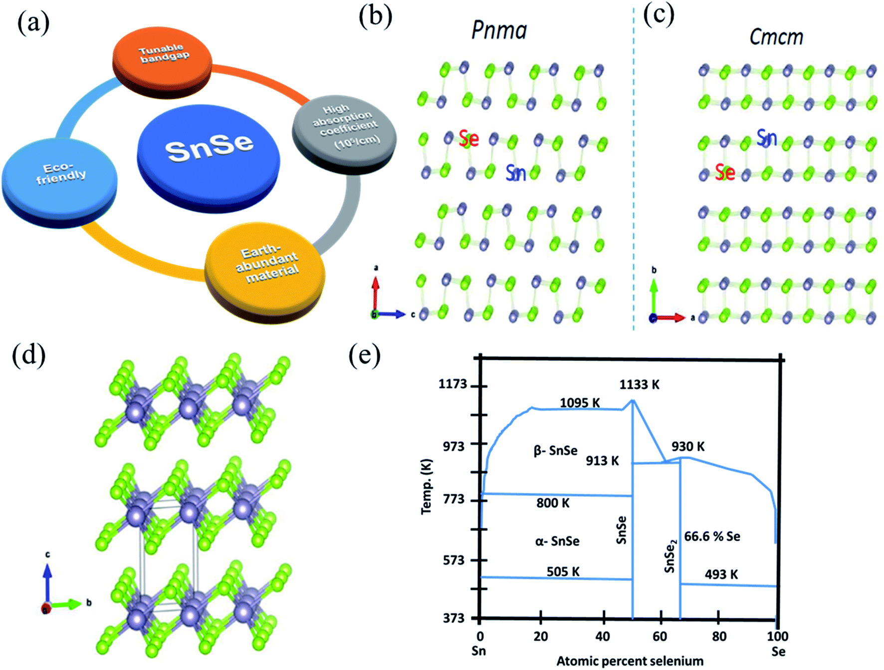 | ||
| Fig. 1 (a) Salient feature of tin selenide materials. (b) Crystal structure of SnSe, (c) SnSe having Pnma to Cmcm phase transition. This figure has been adapted/reproduced from ref. 38 with permission from Elsevier, copyright 2018". (d) Crystal structure of SnSe2. This figure has been adapted/reproduced from ref. 33 with permission from ACS, copyright 2016". (e) Equilibrium phase diagram of Sn–Se system. This figure has been adapted/reproduced from ref. 39 with permission from Wiley, copyright 2020". | ||
Defects present in the material also influences the properties of materials like electronic, magnetic, and optical properties. SnSe is generally a p-type semiconductor. Density functional theory (DFT) calculation is performed to study the defects during SnSe crystal growth. The Sn vacancy is present as a native defect, which causes the p-type conduction in the SnSe under Se or Sn rich conditions, as confirmed by Scanning Tunneling Microscopy (STM) studies.40,41 SnSe2 shows n-type conduction. DFT calculation shows that the vacancy of selenium and interstitial tin led to this n-type conduction in SnSe2.41 The optoelectronic and physical properties of SnSe/SnSe2 materials depend on the growth conditions, size, morphology, phase purity, growth techniques, etc. Therefore, selection of synthesis/deposition method impacts material as well as its proposed applications.
3. Synthesis of SnSe and SnSe2
The material's properties also depend on the growth conditions,42 size, and morphology of the material,43 phase purity,43 defects,44 etc. Various physical and chemical methods have been established to fabricate SnSe/SnSe2 materials on different substrates (glass, flexible metal foil, polymer, etc.) for multiple applications. The tin selenide based semiconductor materials have been synthesized using atomic layer deposition (ALD),17 sputtering,45 thermal evaporation,46 hydrothermal,47 spray pyrolysis,48 chemical vapor deposition (CVD),49 etc.Bulk crystals of the SnSe and SnSe2 can be easily obtained by the physical solid-state reaction method. >99.99 pure elemental powders of the Sn and Se (in the stoichiometric ratio) is taken and sealed in the quartz tube at the pressure of ∼10−4 torr. It is placed at the temperature according to the Sn–Se system phase diagram, as shown in Fig. 2(a). The Bridgman method can be used to obtain single crystals. The powder was melted into the furnace and brought in the contacts with the single crystal's seed during its cooling. The material grows along the crystallographic orientation of the seed crystal. Depending upon the geometry it is called the horizontal Bridgman method or vertical Bridgman method. The Bridgman–Stockbarger technique as shown in (Fig. 2(a)) can be used to obtain a single crystal of SnSe and SnSe2 with an optimized ampule lowering rate of 7 mm h−1 and 4 mm h−1, respectively, for SnSe and SnSe2 with an optimized temperature gradient of 15 °C cm−1.50 Another technique to grow single crystals are the direct vapor transport method,42 and temperature gradient method.51 A detailed review of the growth of the SnSe single crystals can be found in an earlier study.25 Various methods to grow the nanostructure of the SnSe and SnSe2 is described in this section.
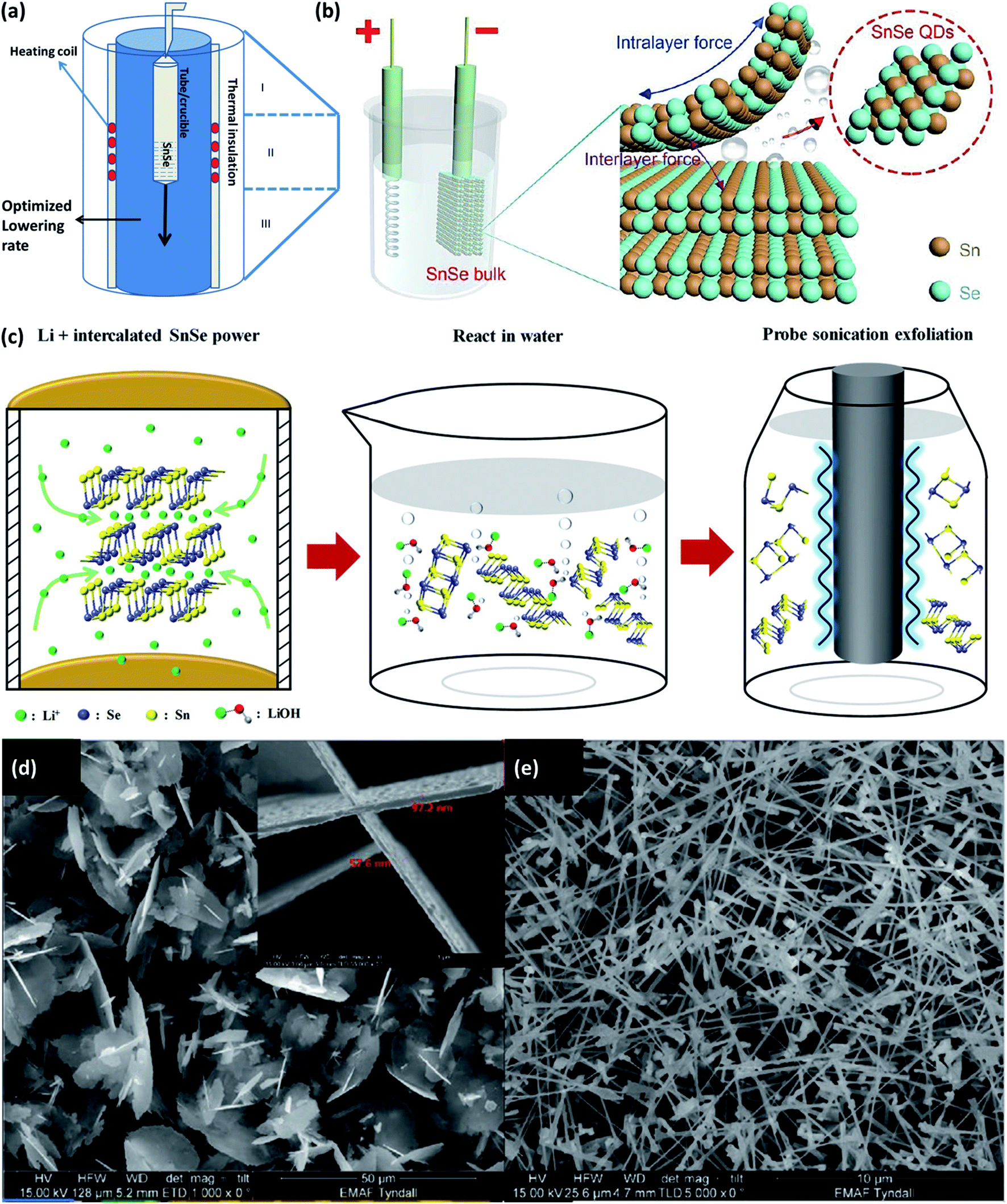 | ||
| Fig. 2 (a) Bridgeman–Stockbarger technique to grow a single crystal. (b) Schematic illustration for the synthesis of SnSe QDs by cathodic exfoliation. This figure has been adapted/reproduced from ref. 52 with permission from RSC, copyright 2019" (c) schematic synthesis process for the SnSe nanosheets by the liquid-phase exfoliation method includes two main steps: Li± hydrothermal intercalation and sonication-assisted exfoliation. This figure has been adapted/reproduced from ref. 54 with permission from Wiley, copyright 2020". SEM images showing the evolution of the SnSex nanostructures concerning the growth temperature, (d) large flakes with diameters of several microns grown at 450 °C, with a thickness of ∼60 nm shown in the inset, (e) high yield of nanowire growth at 500 °C. This figure has been adapted/reproduced from ref. 49 with permission from Wiley, copyright 2020". | ||
3.1 Synthesis of nanostructured SnSe
Li et al.52 devised the facile cathodic exfoliation method to exfoliate SnSe bulk into quantum dots with high yield. Under the organic electrolyte containing 0.2 M of tetra-butylammonium (at −7.5 V for 30 min) bulk SnSe was exfoliated and downsized up to ∼10 nm in lateral size, which was further downsized to ∼4 nm by breaking weakly entangled dots with the help of sonication as shown in Fig. 2(b). To synthesize the SnSe flake up to one layer, Jiang et al.53 reported the two-step process, in which first the bulk SnSe flakes were obtained by the atmospheric pressure vapor transport deposition method. Flash evaporation of SnSe powder was done by moving the quartz tube position containing SnSe powder at 700 °C under Ar/H2 gas pressure under atmospheric condition. SnSe is deposited on the Si substrate kept in upside-down position. As obtained flakes were etched with the N2 gas. Etching time of 5–20 min gave the single layer SnSe flake (thickness of 6.8 Å).53 The SnSe nanosheet of the best quality can be produced from the SnSe bulk powder by the three-step method.54 The method comprises the intercalation of Li+ ion into the SnSe layers by lithification and then reacting the material with water. The rapid expansion of H2 gas during reaction with water exfoliated the SnSe nanosheets. To improve the nanosheets' yield, further sonification of the SnSe powders' residuals is carried out (shown in Fig. 2(c)).Using the precursor diselenoether SnCl4[BuSe(CH2)3SenSeBu]}, SnSex nanostructures are formed on the Si(100) substrate coated with Au (acted as a catalyst) by the liquid injection chemical vapor deposition method, and growth was studied in the temperature range 450–550 °C. Under the 1.1 sccm flow of Ar gas and 1.5 mL h−1 of precursor injection rate, SnSe2 flake growth occurred at 450 °C, and considerable growth of SnSe nanowires occurred at 500 °C as shown in Fig. 2(d) and (e).49
3.2 Synthesis of nanostructured SnSe2
Choi et al.55 synthesized the nano-plates of the SnSe2 by dissolving 5 mL oleylamine in 50 mg, 0.26 mmol SnCl2 at 220 °C.After that, a solution containing 1,3-dimethylimidazoline-2-selenone (90 mg, 0.53 mmol), dichloromethane (4 mL), and oleylamine (2 mL) were mixed and heated for 2 h at this temperature. After that, it was cooled to room temperature, centrifuged, and the residue was washed using hexane to obtain SnSe2 nanoplates. The transmission electron microscopy (TEM) image of SnSe2 nanoplates are shown in Fig. 3(a)–(d).
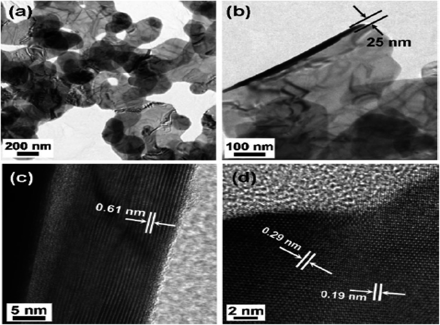 | ||
| Fig. 3 TEM image (a) and (b) SnSe2 nanoplates and high resolution TEM (HRTEM) images (c) side, and (d) top views. This figure has been adapted/reproduced from ref. 55 with permission from RSC, copyright 2011". | ||
A simple two-step method, i.e., sonication followed by laser ablation, was used by Li et al. to obtain SnSe2 quantum dots (QD) from bulk powder.56 Manually grinded SnSe2 powder (20 mg) was dispersed in 30 mL deionized water, and the solution was sonicated (650 W) for 2 h in an ice bath for 4 s. Sonication resulted in smaller particles and flakes of SnSe2. The obtained solution kept in quartz cuvette was irradiated with a 1064 nm laser (Nd:YAG, 2.2 W) for 10 min. Irradiated tiny particles were centrifuged for 30 min at 6000 rpm, resulting in SnSe2 QD, as shown in Fig. 4(a) and (b).
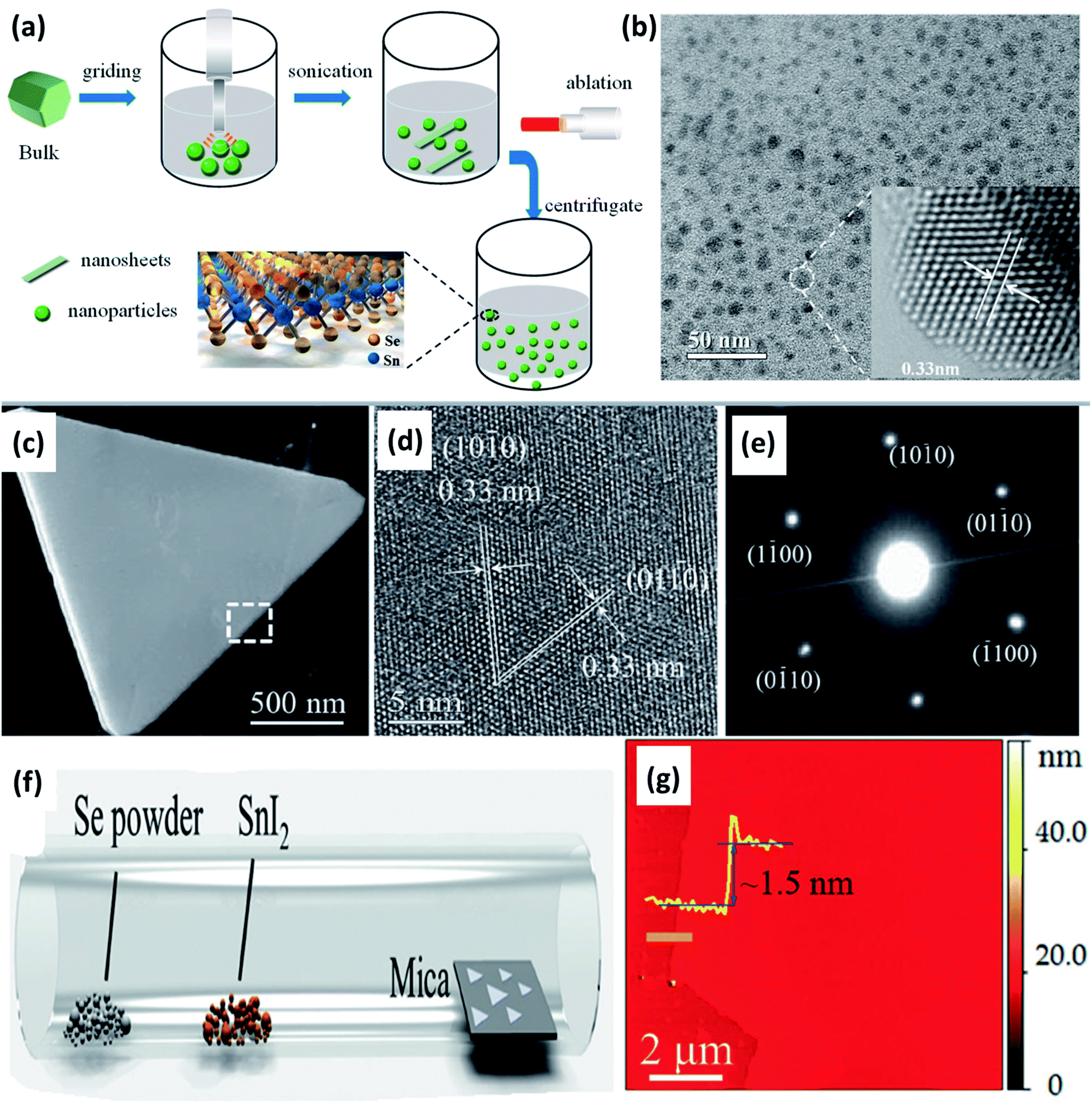 | ||
| Fig. 4 (a) Schematic show of the SnSe2 structure and the quantum dot (QD) fabrication process, and (b) TEM image of SnSe2 QDs with a centrifugal speed of 6000 rpm. These figures has been adapted/reproduced from ref. 56 with permission from MDPI, copyright 2019". (c) Low-magnification TEM image of a SnSe2 flake, (d) corresponding HRTEM image of the flake, (e) electron diffraction pattern from the same flake, (f) schematic diagram of the chemical vapor deposition method, and (g) a typical atomic force microscope (AFM) image at the flake edge, and the height profile showing a thickness of ∼1.5 nm. These figures has been adapted/reproduced from ref. 57 with permission from Wiley, copyright 2015". | ||
Ma et al.58 synthesized the nanorods and nanoplates of the SnSe2 by organic solution phase route. Two different solutions of 0.4 mmol SnCl2·2H2O, 2 mmol oleic acid, 8.5 mL liquid paraffin oil, and 0.4 mmol selenium powder, 9 mL liquid paraffin were used. The first solution was heated at 160 °C till lemon yellow color appeared, and the later solution was heated at 240 °C till wine color appeared. The latter solution was injected into first using syringe rapidly and the mixture was heated at 200 °C for 20 min. After cooling, toluene and methanol was added. After centrifugation nanorods and nanoplates' were obtained. Chemical vapor deposition was employed by Zhau et al. to synthesize ultrathin (1.5 nm) SnSe2 flakes of high quality.57 Low melting point precursor SnI2 (0.01 g) and Se (0.1 g) powders were placed in two different alumina crucible, and mica substrate were placed ∼15 cm from the central zone. The central zone was heated at 600 °C for 15 min, with a flow of H2 (5 sccm) and Ar (20 sccm) at ambient pressure. As-synthesized flakes are shown in Fig. 4(c)–(g).
4. Various applications
In recent times, tin selenide has gained significant research attention for solar cells, thermoelectric, photodetectors, photocatalytic, phase change memory, gas sensing, and anode material for battery, supercapacitor, topological insulator etc. Various reported applications based on SnSe materials are displayed in Fig. 5.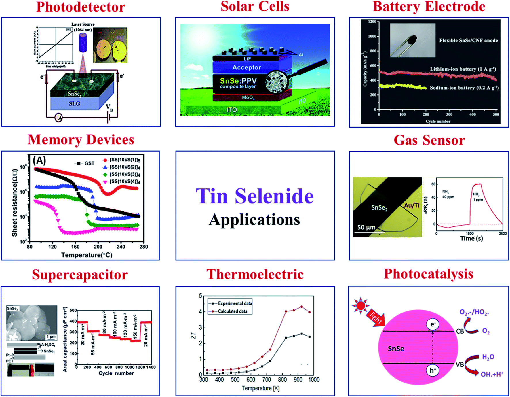 | ||
| Fig. 5 Various applications are based on SnSe materials. Solar cell, this figure has been adapted/reproduced from ref. 59 with permission from ACS, copyright 2010". Battery electrode, this figure has been adapted/reproduced from ref. 60 with permission from Elsevier, copyright 2020". Gas sensor, this figure has been adapted/reproduced from ref. 61 with permission from ACS, copyright 2019". Photocatalysis, this figure has been adapted/reproduced from ref. 62 with permission from Scielo, copyright 2017". Thermoelectric, this figure has been adapted/reproduced from ref. 38 with permission from Elsevier, copyright 2018". Supercapacitor, this figure has been adapted/reproduced from ref. 63 with permission from ACS, copyright 2014". Memory devices, this figure has been adapted/reproduced from ref. 64 with permission from AIP, copyright 2014". And photodetector, this figure has been adapted/reproduced from ref. 65 with permission from Elsevier, copyright 2020". | ||
4.1 Thin film solar cells (TFSCs)
Fabrication of low-cost thin-film solar cells is highly needed as they can also be deposited over flexible substrates. The CuInGaSe2 (CIGSe) and CdTe based solar cells have shown record small cell power conversion efficiency (PCE) of 23.35% and 22.1%, respectively.66 But in CIGS TFSC, indium is rare, and gallium is very costly. In CdTe TFSC, Cd is toxic, and Te is a rare material. These materials related problems hinder the commercialization of low-cost, earth-abundant TFSC based on CISG and CdTe. In recent time, earth-abundant and low-cost compound semiconductor materials like Cu2ZnSnS4 (CZTS), Cu2ZnSnSe4 (CZTSe), and Cu2ZnSn(S,Se)4 (CZTSSe) have gained massive consideration as alternate materials instead of CIGS and CdTe as they have shown the efficiency of 10%, 11.95%, and 12.62%, respectively.67–69 But, kesterite material consists of many elements.70 The presence of many elements in the absorber layer increases the processing cost, and defects are also formed during the processing, which ultimately reduces the overall PCE of solar cells. To overcome this problem, binary element-based materials with similar optical and electronic properties are more suited than quaternary element-based kesterite materials. Tin sulfide (SnSe) is also attracting attention of researchers for optoelectronic device applications. In SnSe, only one impurity phase of SnSe2 is present.71 Therefore, the formation of phase SnSe is easier. Also, being consists of earth-abundant, inexpensive, and eco-friendly elements, SnSe has attracted significant attention. The SnSe has an optimum bandgap of 1.1 to 1.3 eV, an absorption coefficient of ∼105 cm−2, and p-type conductivity with high carrier concentration (1017 cm−3), making it a fabulous material for solar photovoltaic applications.8 Due to its optimum bandgap (1.3 eV) and high absorption coefficient (105 cm−1), a thin layer of 300 nm thickness can absorb most of the useful solar spectrum. The tunable bandgap of thin-film SnSe can help absorb more solar radiation and enable more photon absorption, resulting in more electron–hole pair generation. The theoretical efficiency for material with a bandgap of 1.3 eV is 32%.72 The SnSe thin film can be deposited using various chemical and physical routes like chemical bath deposition (CBD),73 electrodeposition,74 spray pyrolysis,75 atomic layer deposition (ALD),17 thermal evaporation,46 sputtering.76,77The device architecture for SnSe TFSC is SLG/Mo/SnSe/CdS/i-ZnO/TCO/metal grid, similar to CIGS,78 and CZTS/CZTSe/CZTSSe TFSCs.79 Therefore, a lot of modifications and optimizations are required. Also, many issues need to be mitigated to improve efficiency.80 Consequently, it is essential to conduct a study on SnSe material to develop environmentally-friendly, low-cost TFSCs. Any photovoltaic materials should have good optical properties, appropriate band gap, good absorption coefficient, high carrier concentration, and better transport properties. Solar cell efficiency may get affected due to losses, i.e., optical losses, non-absorption, thermalization, reflection loss, transmission loss, area loss, collection losses, and resistance losses.81 However, the formation of pure phase SnSe thin films has not been reported as the phase lies in a very narrow region, and fine compositional tuning is required to achieve SnSe pure phase. Sn and Se's reaction mechanism plays a crucial role in attaining pure phase SnSe thin films.19,82 Reddy et al. studied the effect of selenization temperature, elemental composition, and selenization pressure on SnSe. They observed that the single-phase SnSe thin films could be achieved during the selenization process in the temperature ranges from 300 to 500 °C.77 The solar cell efficiency depends on various parameters, like deposition condition, the absorber's crystallinity, carrier concentration, and the p–n junction's nature. The lower solar cell efficiency based on SnSe thin films may be due to SnSe absorber materials' low quality. The parameters that highly influence SnSe thin film quality are phase purity, higher crystallinity, and larger grain size with fewer pinholes. It has been observed that during SnSe phase formation, there is a possibility of the formation of the SnSe2 phase. Thus, the SnSe2 phase's impact on the solar cell performance of SnSe thin films needs to be carefully studied and optimized.8 The electronic properties of p–n junction interfaces are strongly influenced by the discontinuities between the valence band (VB) maxima and conduction band (CB) minima of each material, which restrict the electron transport across the junction interfaces. Band alignment of SnSe with an n-type buffer layer, the density of defect states at the hetero-junction interface, and the nature of back contact also influence the solar cell performance. Therefore, band offsets play a crucial role in reducing the dark current in a diode, reducing the photon-generated carrier losses, and improving the overall solar cell conversion efficiency. The n-type buffer layer with a wider band gap is needed to overcome the optical losses and provide better alignment with SnSe absorber material.
In 1990, Singh et al. reported SnSe based solar cells with power conversion efficiency (PCE) of 2.3%.75 The fabricated solar cell showed an open-circuit voltage (Voc) of 410 mV, short-circuit current density (Jsc) of 9.20 mA cm−2, and a fill factor (FF) of 49%, respectively. Rahman et al. fabricated heterojunction (p-SnSe/n-Si) solar cells and achieved an efficiency of about 6.44%.83 They observed improved power conversion efficiency due to the improvement in the Jsc with a graded junction.83 Shinde et al. fabricated SnSe thin-film solar cells using electro-deposition and exhibited device efficiency of 1.4% using an absorber film with 300–400 nm-sized grains, uniform, and dense film morphology.73 Franzman et al. synthesized SnSe/PPV (poly[2-methoxy-5-(3′,7′-dimethyl octyl oxy)-1,4-phenylenevinylene]) nanocrystals for solar cells and observed improvement in efficiency from 0.03% to 0.06%.
They observed significant improvement in external quantum efficiency (EQE) and Jsc after adding PPV into the SnSe absorber. Fig. 6(a) and (b) show the high-resolution transmission electron microscopy (HRTEM) image of a single nanocrystal, and selected area electron diffraction (SAED) pattern of SnSe. Fig. 6(c) shows a low-resolution TEM image of SnSe nanocrystals, and Fig. 6(d) shows the schematic device structure of SnSe solar cells.59 In 2012, Mathews et al. reported the first inorganic thin-film solar cell and exhibited a device efficiency of 0.03% (Voc = 140 mV, Jsc = 0.7 mA cm−2). The low device efficiency is mainly due to poor junction quality.74 Makori et al.84 fabricated solar cell with device structure glass/Ag/CdO:Sn/SnSe/Ag by using thermal evaporation and reported device efficiency of 0.59% (Voc = 273 mV, Jsc = 0.993 mA, and FF = 69%). The observed lower efficiency is mainly due to the thin absorber (148 nm) layer, which attributed to lower Jsc in the device. The above discussion is summarized in Table 1.
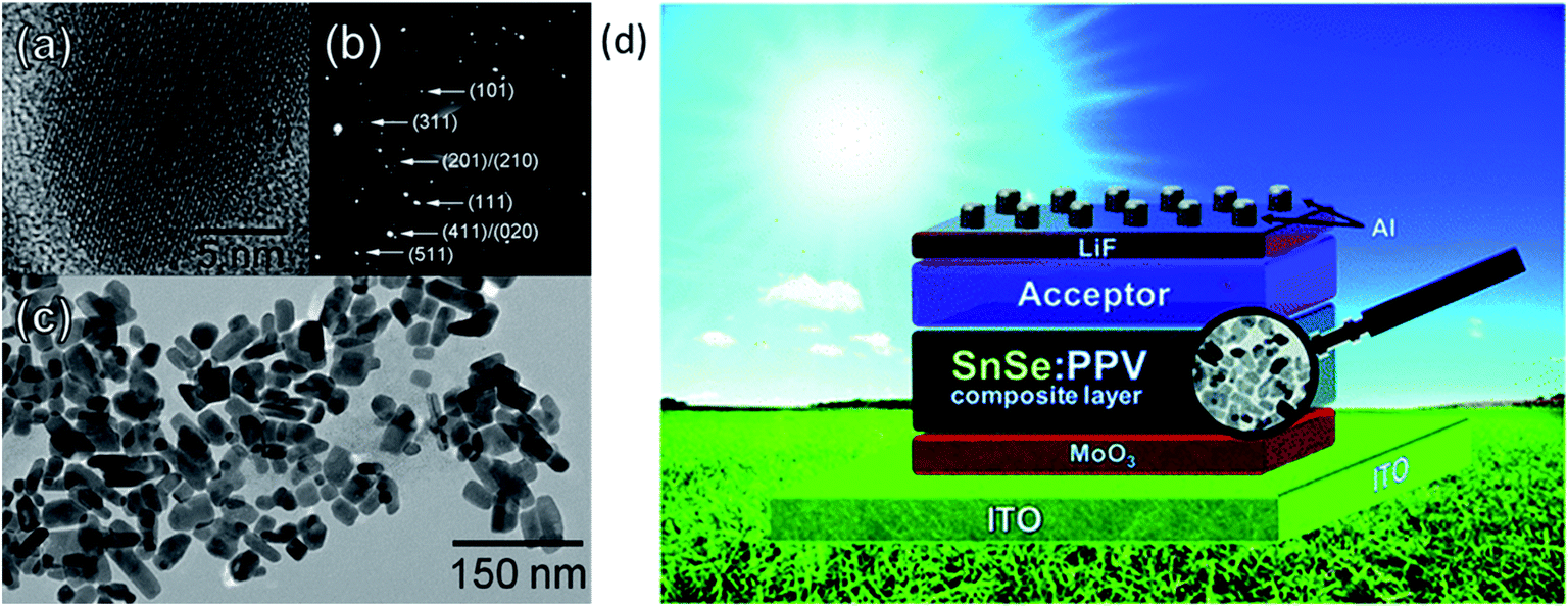 | ||
| Fig. 6 (a) HRTEM image of a single nanocrystal. (b) Selected area electron diffraction (SAED) pattern of SnSe. (c) Low-resolution TEM image of SnSe nanocrystals. (d) The device structure of SnSe solar cells. These figures has been adapted/reproduced from ref. 59 with permission from ACS, copyright 2010". | ||
| Deposition method | Absorber | Device architecture | Voc (mV) | Jsc (mA cm−2) | FF (%) | η (%) | Area (cm2) | Ref. |
|---|---|---|---|---|---|---|---|---|
| Evaporation | SnSe | Si/Al/SnSe/In | 425 | 17.23 | 44 | 6.44 | 0.2 | 83 |
| Evaporation | SnSe | SLG/FTO/Se/SnSe/Ag | 410 | 9.20 | 49 | 2.30 | — | 75 |
| Electro-deposition | SnSe | ITO/CdS/SnSe/Au | 370 | 5.37 | 30 | 1.40 | — | 73 |
| Co-evaporation | SnSe | SLG/Mo/SnSe/CdS/ | 172 | 18.87 | 31.2 | 1.02 | 0.42 | 10 |
| i-ZnO/ITO/Ni–Al | ||||||||
| Sputtering | SnSe | Glass/Ag/CdO:Sn/SnSe/Ag | 207 | 0.90 | 0.69 | 0.59 | — | 84 |
| Electrodeposition | SnSe | Tec15/CdS/SnSe/carbon-paste | 140 | 0.7 | 31 | 0.03 | 0.15 | 74 |
Table 1 shows that the efficiency of SnSe based solar cells is well below Cu2ZnSn(S,Se)4.85 The observed lower efficiency is mainly due to bulk defects, secondary phase formation in SnSe, non-ideal band-alignment at heterojunction interfaces, and back and front electrode recombination. The absorber quality plays a significant role, and a sound absorber should have a dense, pinhole-free, smooth surface of the film for high-efficiency heterojunction device applications. The low interfacial quality could primarily affect the device performance and is responsible for lower Voc and FF in the solar cells. This is mainly due to CB discontinuity/band offsets at the interfaces, which leads to the CB's energy barrier and restricts carrier transportation across the p–n junction. Apart from this, absorber thickness, grain size, bandgap, and deposition methods also influence the device performance.
4.2 Thermoelectric generators
It requires energy to maintain the sustainability and development of humankind. Energy sources are minimal, and there arises a question about the world's power crisis and its ultimate solution. A thermoelectric device that can convert the waste heat into electricity can contribute to a remarkable extent in this.SnSe single crystal. With the report of a high ZT value of 2.6 along the b axis in single-crystal SnSe,32 this material became the hot topic of research in the field of thermoelectric (TE) domains since 2014. SnSe is anisotropic and exhibits the second-order displacive phase transition from Pnma (distorted) to Cmcm (non-distorted) at 750–800 K. It shows a moderate power factor of 10.1 μW cm−1 K−2 at ∼850 K along the b axis, which is comparable or even lesser than typical thermoelectric materials values.86–89 The thermal conductivity of SnSe has astonished the researchers. Using the Gruneisen parameter, it has been estimated that SnSe exhibits the ultra-low thermal conductivity (<0.25 W m−1 K−1) due to the strong anharmonicity in bonding.32 Theoretical studies90,91 showed that optimized carrier concentration lies in the range 1019–1020 cm −3 for SnSe for high ZT. For n-type SnSe, the estimated ZT is 3.1 along a axis at 770 K at carrier concentration of 2.8 × 1019 cm−3, while the study showed that the n-type SnSe performed better than p-type SnSe.92
Motivated by the high ZT along the b axis in SnSe, Li et al.38 conducted the theoretical study on the p-type SnSe using the first-principle calculation. A figure of merit (ZT) was greatly affected by the carrier concentration and also sensitive to the phases of SnSe (Pnma and Cmcm) (shown in Fig. 7(a) and (b)). Fig. 7(c) shows a comparison of theoretical and experimental data.32 This study showed that a maximum ZT of 4.33 could be achieved for the Cmcm phase of SnSe at 923 K for carrier concentration of 1.84 × 1019 cm−3, along the b axis.
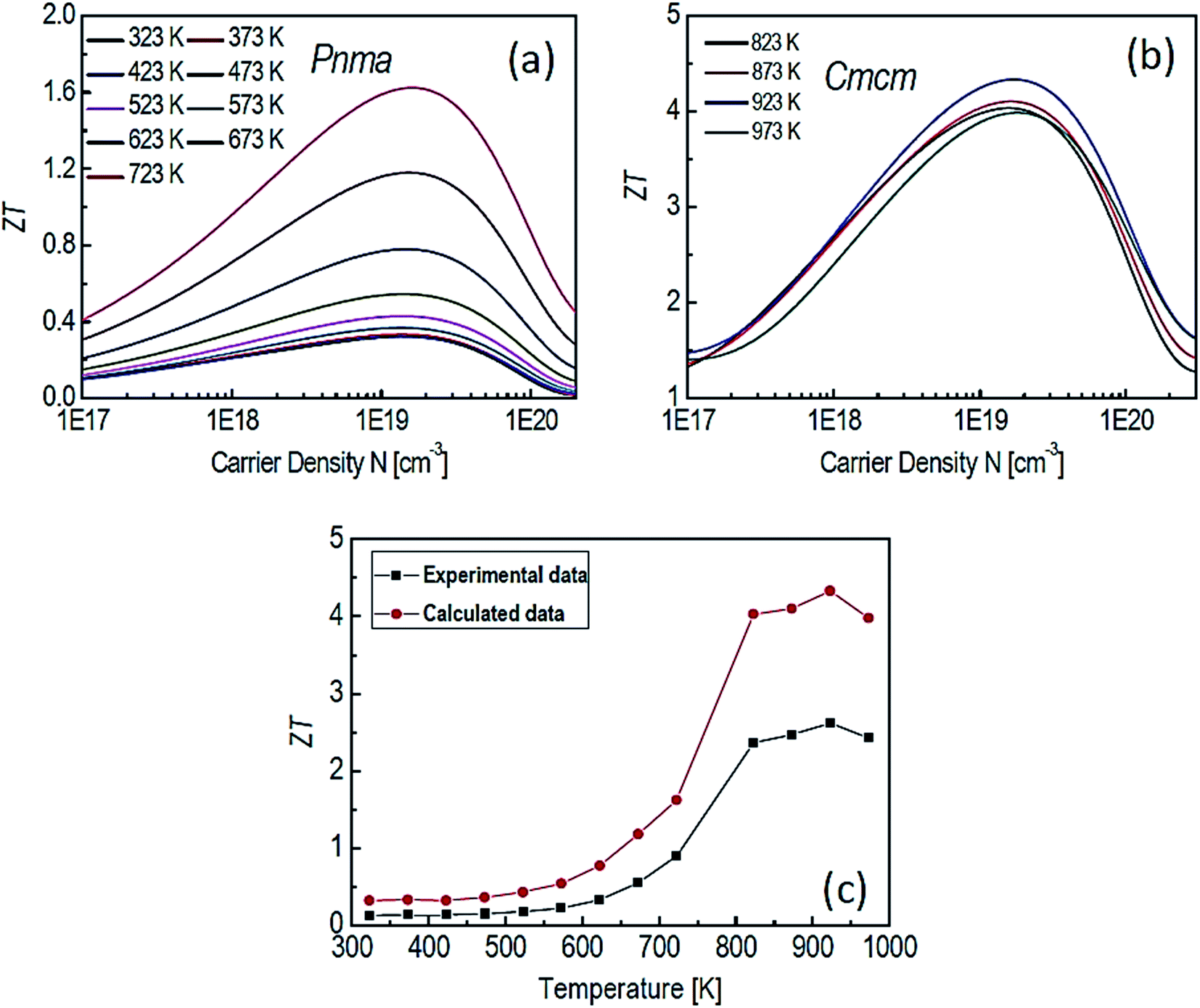 | ||
| Fig. 7 The ZT of SnSe for Pnma (a), Cmcm (b) phases and comparison between experimental data32 and calculated data (c). These figures has been adapted/reproduced38 with permission from Elsevier, copyright 2018". | ||
Through another study, for Na doped SnSe single crystal, Zhao et al. reported the device with ZTdevice = 1.34 in the temperature range 300–773 K. With ZTmax. of 2.0 at 773 K, the device showed the conversion efficiency of ∼16.7%, which was higher than many Pb-based thermo-electric modules.93 Various researchers showed different ZT values for the single crystal. For example, Wei et al.94 showed ZT of ∼1, ∼0.8, and ∼0.25 along b, c, and a axis, respectively for in-house made fully dense single-crystalline SnSe, Jin et al.95 showed ZT ∼ 1 for single crystal grown by a vertical vapor deposition method. Different types of doping are being done to enhance the single-crystal performance. Chang et al.96 doped bromine to make the SnSe conduction n-type and achieved record high ZT ∼ 2.8 ± 0.5 at 773 K along out of the plane direction. With the help of density functional theory and scanning tunneling microscopy, they pointed out that delocalized p electrons of Sn and Se near conduction band minima contribute more to orbital overlapping in out of the plane direction. The S doping in single-crystal SnSe decreased the carrier concentration due to charge trapping at grain interface.97 Hence, S doping decreased the single crystal's thermoelectric performance rather than enhancing as predicted by theoretical calculation.98 Pb doped n-type single crystal (via facile Sn-flux method) showed a 33% enhanced power factor than its pristine SnSe due to increased carrier concentration.99 Ag-doped single crystal (Sn0.97Ag0.03Se) grown in a horizontal Bridgman furnace showed maximum ZT ∼ 0.95 along a axis at 793 K.100 Bi doping in single-crystal SnSe resulted in n-type conduction and showed the remarkable ZT ∼ 2.2 along the b axis at 733 K.51
Polycrystalline SnSe thermoelectric. Polycrystalline SnSe has comparably higher thermal conductivity and lower electrical conductivity than its single crystal counterpart. Though phonon scattering is reduced mainly by the grain boundaries,101 it has higher thermal conductivity than its single crystal due to tin oxide layer102 or absorption of oxygen.103 Highly discrete values of ZT have been reported for polycrystal SnSe made by different growth techniques. Various researchers have tried to achieve a comparable result to a single-crystal. Many researchers chose to dope (Na, K, Cu, Zn, etc.) in poly-crystal SnSe to enhance the electrical properties and reduce the thermal conductivity effectively. In one study, the polycrystalline SnSe thermoelectric material showed ZT ∼ 0.5 at 823 K.104 Several methods improve the device's thermoelectric performance, like large mass fluctuations, band gap engineering, alloying, doping, nano-structuring, etc.105 Gong et al.47 studied the effect of Cu doping in polycrystalline SnSe by varying the concentrations in the CuxSn1−xSe from x = 0.01 to 0.004. They found that Cu doping enhanced the electrical conductivity due to the increased carrier concentration, as confirmed by Hall measurement. Still, Cu doping acted as a point defect and hence decreased the carrier mobility. The Seebeck coefficient also increased due to doping. Thus, the overall power factor increased due to doping, and the optimized value was obtained for doping x = 0.01. Around 60% reductions in the lattice thermal conductivity as compared to undoped poly-crystal SnSe is observed. This was due to nano-precipitation and mesoscale grains (as evidenced by high-resolution transmission electron microscopy (HRTEM)). Finally, they achieved a ZT of 1.2 at 873 K. Shi et al.106 enhanced the Cu's solubility limit in the SnSe and obtained the ZT of ∼1.41 for the doping level of x = 0.118.
Lee et al.102 synthesized polycrystalline SnSe (Na0.01(Sn0.95Pb005)0.99Se), which exhibited ZT ∼ 2.5 at 773 K. They noticed that the oxide formation leads to higher thermal conductivity in poly-crystal SnSe (SnO2 has ∼140 times higher thermal conductivity than SnSe).107 They removed the oxides layers of the tin in SnSe by Ball milling followed by a reduction in 4% H2/Ar atmosphere for 6 h at 613 K. They pointed out that ball milling (BM) and reduction processes both are critically important to remove the oxides and its residuals from the sample. A remarkably ultralow thermal conductivity (total) of 0.20 W m−1 K−1 (even lower than the single crystal reported by Zhao et al.32 ) (Fig. 8(a)) and ∼2 times enhanced power factor than the pristine SnSe (unball-milled and unreduced). The performance of pristine, reduced, ball-milled and reduced (BR) compared to with the single-crystal SnSe32 and Na doped SnSe,93 is shown in Fig. 8(b). Recently Gainza et al.108 reported the highest ZT of 1.8 for the un-doped polycrystalline SnSe, and even with surface oxides layers on the sample.
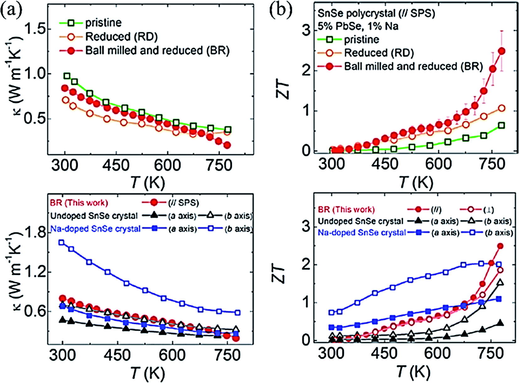 | ||
| Fig. 8 (a) Total thermal conductivity of polycrystalline SnSe–PbSe (5 mol %) doped with 1 mol% Na for pristine, Reduced (R), and Ball milled then Reduced (BR) samples taken parallel to the press direction of SPS, and total thermal conductivity compared with undoped SnSe32 and Na doped SnSe,93 and (b) ZT of polycrystalline SnSe–PbSe (5 mol %) doped with 1 mol% Na for pristine, Reduced (R), and Ball milled then Reduced (BR), and ZT compared with the undoped SnSe32 and Na doped SnSe.93. These figures has been adapted/reproduced from ref. 102 with permission from Elsevier, copyright 2019". | ||
The pressure-induced effect modifies the textures of the poly-crystal SnSe. A sintering pressure of 60 MPa leads to improved electrical properties. There was a meager improvement in thermal conductivity, resulting in a ZT of 0.7.109 There is a vast literature on doping in the polycrystalline SnSe, like Na,110 K,111 Cd,112 Ag,113 and co-doping Na/Ag,114,115 Bi/Cl,116 Na/CNT,117 etc. which resulted in the enhancement in the thermoelectric performance of the material. Lu et al.118 enhanced the performance of polycrystalline SnSe by introducing large mass fluctuations by doping sulfur, which led to very low lattice thermal conductivity (0.13 W m−1 K−1 at 873 K). Still, this doping enhanced the bandgap of the SnSe, which lowered the electrical conduction and hence the power factor (low carrier concentration due to large bandgap). Pb co-doping improved the power factor, further increasing the carrier concentration by one order of magnitude. Through co-doping a remarkable ZT of 1.85 at 873 K was achieved. The inclusion of micro carbon fibers into the polycrystalline SnSe decoupled the thermal and electrical transport in the host matrix. Carbon fibers acted as good electrical conductors and simultaneously reduced the lattice thermal conductivity (0.22 W m−1 K−1) by enhancing the scattering due to the high density of interface, which led to ZT ∼ 1.3 at 823 K. This inclusion increased the mechanical stability of the device.119 The thermoelectric parameters of poly-crystals SnSe are tuned by sintering temperature in the spark plasma sintering (SPS). Zhang et al.120 varied the sintering temperature from 300 to 650 °C in SPS and showed that vacancy defects (Se, Sn, and Se–Sn) were responsible for the performance variation.
The optimized sintering temperature for the best performance of the material was 550 °C. The ZT of 0.47 was observed at 430 °C. Ge alloying's effect was studied by varying Ge concentration in the range x = 0.01 to 0.03 (Sn1−xGexSe). The carrier concentration increased from 3.9 × 10¹⁷ to 4.2 × 1019 cm−3 for x = 0.03, which resulted in a high-power factor of ∼5.10 μW cm−1 K−2 at 873 K. A very low lattice thermal conductivity of ∼0.18 W m−1 K−1 was achieved due to nanoscale grains, precipitation and anharmonicity due to Ge doping. Finally, high ZT of 1.75 and 2.1 were acquired at 873 K along parallel and perpendicular SPS's pressing direction.121 The figure of merit (ZT) with different doping elements in single and polycrystal SnSe is shown in Fig. 9.
 | ||
| Fig. 9 Variation of ZT with the doping element given in bracket, where blank () shows the undoped SnSe. | ||
SnSe thin film. Low temperature (4–300 K) thermoelectric measurements were carried out by Urmila et al.122 in SnSe thin-film obtained by the co-evaporation method. The maximum power factor obtained was 7.2 × 10⁻⁴ W m−1 K−2. The thermal conductivity was in the range of 0.023 to 0.045 W m−1 K−1, which showed a maximum ZT of 1.2 at 42 K, and thus showed a potential application in a low-temperature TE device. Nair et al.123 fabricated the n–p type thermo-couples with PbSe (p-type), SnSe (p-type), and SnSe2 (n-type), in the configuration SnSe–SnSe2–SnSe–SnSe2–SnSe and PbSe–SnSe2–PbSe–SnSe2–PbSe using chemical method. A voltage was developed for a temperature difference of 20 °C of magnitute 50 mV and 15 mV, respectively (the author did not report the ZT of the device). Thin-film SnSe deposited by glancing angle (80°) pulsed laser revealed a striking power factor of 18.5 μW cm−1 K−2 at 478 K (higher than the single crystal along b axis) due to enhanced grain boundaries and out of plane thermal conductivity (highest 0.189 W m−1 K−1 at 340 K). The authors did not report the ZT and in-plane thermal conductivity.124 For the first time, Burton et al.125 reported thin film SnSe thermoelectric generator on the glass substrate. Very low thermal conductivity of 0.08 W m−1 K−1 in the temperature range 375 to 450 K was observed (4 times lower than single-crystal thermal conductivity along a-axis). Still, it had a low power factor, which resulted in a very low ZT of 0.055 at 501 K. When the hot side was kept at 618 K, an output of 0.09 μW was achieved. Due to the oxide formation and uncontrolled cold side temperature, the performance degraded for a longer exposure. Song et al.126 synthesized SnSe thin film of varied thickness in the range of 600–1000 nm by magnetron sputtering and showed effect of post-annealing on the performance. The optimized annealing temperature was 700 K. The power factor for the film with thickness 700 nm was 2.4 μW cm−1 K−2 at 675 K. The authors used the thermal conductivity data of bulk polycrystalline SnSe to calculate the ZT (0.28 at 675 K). Yan et al.127 fabricated a flexible thermoelectric device based on SnSe composite with PEDOT:PSS that showed 13.73 nW output power at 50 K temperature difference at 353 K, and showed possible application in wearable electronics as well due to stability of device even after 1000 cycles of bending. The above discussion is summarized in Table 2.
| Material | Synthesis method | Power factor (μW (cm−1 K−2)) | Thermal conductivity (W m−1 K−1) | Temp. (K) | ZT | Ref. |
|---|---|---|---|---|---|---|
| Pristine SnSe (single crystal) | Bridgman Crystal growth | ∼9 | 0.34 | 923 | 2.62 | 32 |
| Single crystal | Vertical Bridgman | 8.5 | — | 850 | 1 | 128 |
| Single crystal | Vertical vapor deposition | 5.23 | 0.44 | 800 | 1 | 95 |
| Na doped SnSe single crystal | — | ∼14 | ∼0.55 | 773 | ∼2 | 93 |
| Br doped SnSe single crystal | Temperature gradient | ∼9 | ∼0.23 | 773 | 2.8 | 96 |
| S doped single crystal | Direct vapor transport | 0.0011 | — | 573 | 0.0012 | 97 |
| Pb doped SnSe single crystal | Flux method | 1.2 | — | 300 | — | 99 |
| Ag-Doped SnSe single crystal | Horizontal Bridgman method | ∼5.7 | 0.49 | 793 | 0.95 | 100 |
| Bi-Doped SnSe single crystal | Temperature gradient | ∼9.75 | ∼0.3 | 733 | 2.2 | 51 |
| Polycrystal SnSe | Solid state reaction (SSR) | ∼4 | <0.5 | 823 | 0.5 | 129 |
| Polycrystal SnSe | Arc melting | ∼10 | ∼0.4 | 816 | 1.8 | 108 |
| Cu doped polycrystal SnSe | Hydrothermal | 3.4 | 0.26 | 873 | 1.2 | 47 |
| SnSe0.98Te0.02 | — | ∼4 | ∼0.35 | 805 | 1.05 | 130 |
| Sn0.97Gd0.03Se | Hydrothermal | 6.7 | 0.4 | 868 | ∼1 | 131 |
| Sn0.985S0.25Se0.75 | Mechanical alloying | 4.5 | ∼0.35 | 823 | 1.1 | 132 |
| Sn0.978Ag0.007S0.25Se0.75 | 5.3 | ∼0.25 | 823 | 1.75 | ||
| Sn0.90Pb0.15Se0.95Cl0.05 | SSR | 6.74 | 0.5 | 823 | 1.2 | 133 |
| Cu doped polycrystal SnSe | Solvothermal | 5.57 | 0.32 | 823 | 1.41 | 106 |
| Na, Pb doped polycrystal SnSe | SSR | 6.85 | 0.20 | 773 | 2.5 | 134 |
| Polycrystal SnSe | Mechanical alloying | 3.9 | — | 823 | 0.7 | 109 |
| Na doped SnSe polycrystal | SSR | 4.5 | ∼0.4 | 773 | 0.8 | 110 |
| K doped SnSe polycrystal | Mechanical alloying | ∼2.9 | ∼0.22 | 773 | 1.1 | 111 |
| Cd doped SnSe polycrystal | Solvothermal | 6.9 | 0.33 | 823 | 1.7 | 112 |
| Ag doped polycrystal SnSe | Facile surfactant-free synthesis | 6.34 | 0.75 | 850 | 0.8 | 113 |
| Ag/Na doped polycrystal SnSe | — | ∼7.5 | ∼0.5 | 773 | 1.33 | 114 |
| Ag/Na doped polycrystal SnSe | SSR | 5 | ∼0.48 | 773 | 0.81 | 115 |
| CNT dispersed Na doped polycrystal SnSe | SSR | 4.99 | 0.40 | 773 | 0.96 | 117 |
| S, Pb doped polycrystal SnSe | Hydrothermal | 4.18 | ∼0.20 | 873 | 1.85 | 118 |
| Composite of carbon fiber and polycrystal SnSe | SSR | 3.88 | ∼0.22 | 823 | 1.3 | 119 |
| SnSe polycrystal | Solvothermal | ∼4.4 | ∼0.7 | 703 | 0.47 | 120 |
| Ge doped polycrystal SnSe | Hydrothermal | 5.1 | ∼0.21 | 873 | 2.1 | 121 |
| Thin film SnSe | Reactive evaporation | 7.2 | ∼0.023 | 42 | 1.2 | 122 |
| SnSe thin film | PLD | 18.5 | — | 478 | — | 124 |
| SnSe thin film | Thermal evaporation | 0.11 | ∼0.11 | 501 | 0.055 | 125 |
| SnSe thin film | Sputtering | 2.4 | 675 | 0.28 | 126 | |
| SnSe thin film | Chemical vapor transport | — | 0.7 | 300 | 0.16 | 135 |
| SnSe thin film | Chemical vapor deposition | 3.2 | 1.1 | 550 | 0.15 | 136 |
| SnSe/PEDOT:PSS thin film | Vacuum filtration method | 0.24 | — | 353 | — | 127 |
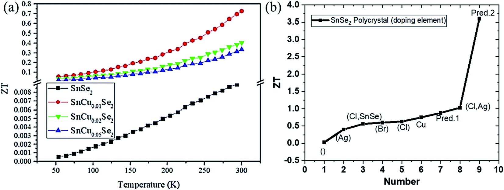 | ||
| Fig. 10 (a) Figure of merit (ZT) of SnCuxSe2 (x = 0, 0.01, 0.02, 0.05) as a function of temperature. This figure has been adapted/reproduced from ref. 145 with permission from ACS, copyright 2020". (b) Variation of ZT with different doping elements, irrespective of operating temperature, where blank () represents undoped SnSe2, and Pred. 1 and Pred. 2 mean theoretical predicted values, respectively. | ||
Thin-film SnSe2 thermoelectric. Thermoelectric performance of SnSe2 thin films have also been studied. But there are very few reports on this, and the reports are limited to the film's power factor only. Yin et al. deposited SnSe2 thin-film on a glass substrate by spin coating techniques and reported a Seebeck coefficient of ∼126.3 μV K−1. The electrical conductivity of the order of 103 S m−1 at room temperature was observed.146 Chen et al. deposited the SnSe thin film on the Si wafer and annealed it in Se vapor. The film was reduced to SnSe2 and showed enhanced Seebeck coefficient 631 μV K−1 for SnSe2 than 38.6 μV K−1 for SnSe. Around 44 times enhanced power factor (0.2 μW m−1 K−2) was obtained.147 Duong et al. deposited SnSe2 thin film on the Al2O3 substrate by the pulsed laser deposition technique. They reported a power factor of 8 μW m−1 K−2 at 220 K.148 A detailed summary of the above discussions and ZT variation with the doping is provided in Table 3 and Fig. 10(b), respectively.
| Material | Synthesis method | Power factor (μW cm−1 K−2) | Thermal conductivity (W m−1 K−1) | Temp. (K) | ZT | Ref. |
|---|---|---|---|---|---|---|
| Cl doped SnSe2 | Facile low-temperature solution | 1.46 | ∼0.45 | 610 | 0.22 | 138 |
| Cl doped SnSe2 | Solid-state reaction followed by hot press | ∼7.0 | ∼1.6 | 673 | 0.4 | 139 |
| Cl doped SnSe2 | Solid-state reaction followed by ball milling and SPS | ∼8 | ∼1.2 | 673 | 0.63 | 140 |
| Ag-Doped SnSe2 | Mechanical alloying followed by SPS | 3.50 | <1 | 773 | 0.4 | 141 |
| Br doped SnSe2 | Solid-state reaction followed by quenching and hot press | — | — | 750 | 0.6 | 142 |
| Cl doped SnSe–SnSe2 | Solid state reaction | — | 0.42 | 773 | 0.56 | 143 |
| Ag and Cl doped SnSe2 | Bottom up | 7.46 | 0.57 | 789 | 1.03 | 149 |
| Cu embedded SnSe2 | Solid-state reaction followed by ball mill and SPS | 1.96 | 0.81 | 300 | 0.75 | 145 |
This material (SnSe) has the highest efficiency among the bulk materials without any doping, but it faces commercialization issues like poor mechanical stability and low thermoelectric property below ∼800 K. Besides its high ZT, low cost, easy fabrication, and earth-abundance, SnSe suffers the real possible application likely due to the quick oxides' formation or thermal instability.150 It readily forms the oxides in the range >600 °C, where it showed maximum ZT. Protective environment costs hamper its effectiveness as a cheap/high ZT. Sassi et al.129 showed thermal instability above the phase transition temperature of SnSe, and the working efficiency of the device decreased continuously over cyclic performance due to Se loss. Thus, there should be an optimized temperature range over which there is no loss of performance. Continuous research should go on in the direction to improve the thermal stability up to the temperature for which SnSe showed maximum ZT. Also, large phonons scattering centers exists in polycrystalline SnSe than in single crystal SnSe due to grain boundaries, yet single crystal SnSe has lower lattice thermal conductivity than the polycrystalline SnSe. Ibrahim et al.151 noted this fact and investigated the reason behind this. They systematically discarded the oxide formation and found many native defects in the single crystal.152 Their results reflected higher lattice thermal conductivity than the reported one.32 They also noted that the single crystal grown by Zhao et al.32 was not fully dense and hence may be the reason for low lattice thermal conductivity. But it still requires the study to know the exact causes of the very low lattice thermal conductivity, whether it was due to intrinsic defect or not. SnSe single crystal suffers a low mechanical strength and high growth cost as a single crystal. SnSe single crystal thermoelectric results showed inconsistencies in the different group reports' as shown in Table 2. However, the further study required to unravel the SnSe performance, where it seeks the possibilities of enhancement in ZT.38 Another phase, SnSe2, was also predicted by theoretical consideration as the best thermoelectric material that can achieve ZT around 3.5. Till date, ZT ∼ 1.1 is achieved in this material. Also, both materials (SnSe and SnSe2) showed inferior TE property in thin film form. Thus, this material demands greater attention and research to achieve predicted ZT. Researchers should pay attention to new approaches to improve the SnSe thermoelectric material's performance like nano-inclusion,153 decoupling of interrelated parameters,119 nano-structuring and texturing, etc. Simultaneously, the theoretical study should be carried out to optimize the threshold values of the parameters. Finally, tin-selenide has emerged as a futuristic material that showed the best efficiency. Both materials (SnSe and SnSe2) demand more research in the thin film and bulk thermoelectric form because of the inferior TE property and device stability.
4.3 Photodetectors (PDs)
 | ||
| Fig. 11 Schematic working state (a) and energy band diagram (b) of the device under the combined action of light illumination and cooling (I1L = photovoltaic current, I2C = thermocurrent). Reprinted with permission from. These figures has been adapted/reproduced from ref. 163 with permission from Elsevier, copyright 2019". | ||
When the Ag side is heated w.r.t. ITO with 4.5 K difference, the opposite result was observed, i.e., there was a decrease in photocurrent and voltage. Hence authors concluded that the coupling of the effect is polarity dependent. Record high value (comparable to the commercialize Ge and Si photodetectors) of responsivity (R) and detectivity (D) were reported in the nanowire SnSe.164 Above discussions have been summarized in Table 4.
| Device structure | λ (nm) | Bias (V) | R (A W−1) | D (Jones) | Response/recovery time (s) | Ref. |
|---|---|---|---|---|---|---|
| ITO/SnSe/ITO | White light | 5 | — | — | 3 | 165 |
| Pd/n-Si/SnSe/Pd | 780 | — | — | — | 0.9/17.3 × 10−6 | 157 |
| Bi2Te3/SnSe/Bi2Te3 | 370 | 20 | 5.5 | 6 × 10¹⁰ | — | 166 |
| Au/SnSe/graphene/Au | White light | 15 | — | — | 1/<1 | 159 |
| Ag/Si/SnSe/graphene oxide QD/Ag | 650 | — | — | — | 0.18/0.75 | 160 |
| Pd/SnSe/Si/In | 850 | 0 | 0.566 | 4.4 × 10¹⁰ | 1.6/47.7 × 10−6 | 167 |
| Gr/SnSe/Gr | 400 | 1 | 0.038 | — | ∼0.18 | 161 |
| Ag/Si/SnSe/Ag | 404 | 15 | 277.3 | 7.6 × 10¹¹ | 0.35/1.83 | 168 |
| ITO/n-SnSe/Ag | 760 | 0 | 3.97 × 10⁻³ | — | 81/122 × 10−6 | 163 |
| Cr/Au/Si/SnSe (nanowire)/Cr/Au | 830 | 3 | 1.0 × 10⁴ | 3.3 × 10¹² | 460/520 × 10−6 | 164 |
| Mica/In2Se3/SnSe/Au | 405 | 5 | 0.350 | — | 0.156/0.139 | 169 |
| Si/SiO2/WSe2/SnSe/Ti/Au | 1064 | 5 | 6.6 × 10⁻³ | — | — | 170 |
| 671 | 31.8 × 10⁻³ | — | ||||
| 457 | 99 × 10−3 | 0.0082/0.0084 | ||||
| PCB/Mica/SnSe (nanocrystal)/Ag | (Sunlight) | 2 | 0.54 × 10⁻³ | 1.06 × 10⁹ | 1.5/1.7 | 171 |
| PET/SnSe/Pd | 404 | 20 | 1745.5 | ∼4.2 × 10¹² | 1.7/4.7 | 172 |
| 850 | 78.6 | ∼9 × 10¹¹ | 0.23/0.27 |
![[thin space (1/6-em)]](https://www.rsc.org/images/entities/char_2009.gif) 176 (which have deeper conduction minima than these) so efficiently that it improved performance parameters several times better. SnSe2 with MoS2 interface resulted in enhanced responsivity from 37.3 to 9.1 × 10³ A W−1 under 500 nm illumination.176
176 (which have deeper conduction minima than these) so efficiently that it improved performance parameters several times better. SnSe2 with MoS2 interface resulted in enhanced responsivity from 37.3 to 9.1 × 10³ A W−1 under 500 nm illumination.176Mukhokosi et al. studied the thickness-dependent optical properties of the SnSe2 thin film grown by DC sputtering followed by selenization and also studied the photodetection performance (Fig. 12(a) and (b)).30 Films with thickness <140 nm did not show any IR response. The film with 1200 nm thickness had a slow response (time), and responsitivity was 0.4 mA W−1.30 Mukhokosi et al.177 also reported the self-powered, organic–inorganic hybrid heterostructure PD consisting of poly (3,4-ethylene dioxythiophene):poly(styrene sulfonate) (PEDOT:PSS) and SnSe2. The device had responsivity in the range of 1.4–2.6 μA W−1. The response time improved to 1.33 s. Mukhokosi et al.178 reported highly enhanced response time and enhanced responsivity. The device was fabricated on the p-type Si substrate by DC sputtering, followed by selenization. Kumar et al.65 deposited SnSe2 thin-film on the soda-lime glass substrate and reported the improved responsivity at very low bias and fast response time in the IR range (Fig. 12(c) and (d)). Although the band gap was in the visible region, photodetection was observed in the IR region which was attributed to the defect/trap assisted levels lying in the forbidden region.65 Usually, SnSe2 shows high absorption coefficient30,65 but poor chemical stability against environmental conditions (degrade into SnSe after prolonged exposure). Therefore, Gao et al. used graphene (Gr) to improve the chemical stability. SnSe2 was sandwiched between graphene. Monolayer Gr acted as useful ohmic contacts and also had weak absorption in the UV to IR range.179 This sandwiched structure of SnSe2 with Gr showed responsivity of 1.09 × 10³ A W−1, and the response time was 30 ms. Murali et al. studied the substrate-induced effect on SnSe2 flake (i) suspended over contacts and (ii) supported on Si substrate. It showed a vast difference in rise and decay times.180 The suspended structure showed low gain but quicker decay than the supported one because of the device's interface-induced trap states. Field-effect transistors based on multilayer SnSe2 showed very high responsivity and detectivity. The device showed its potential application comparable to the other commercialized photodetector.9 The above discussion is summarized in Table 5.
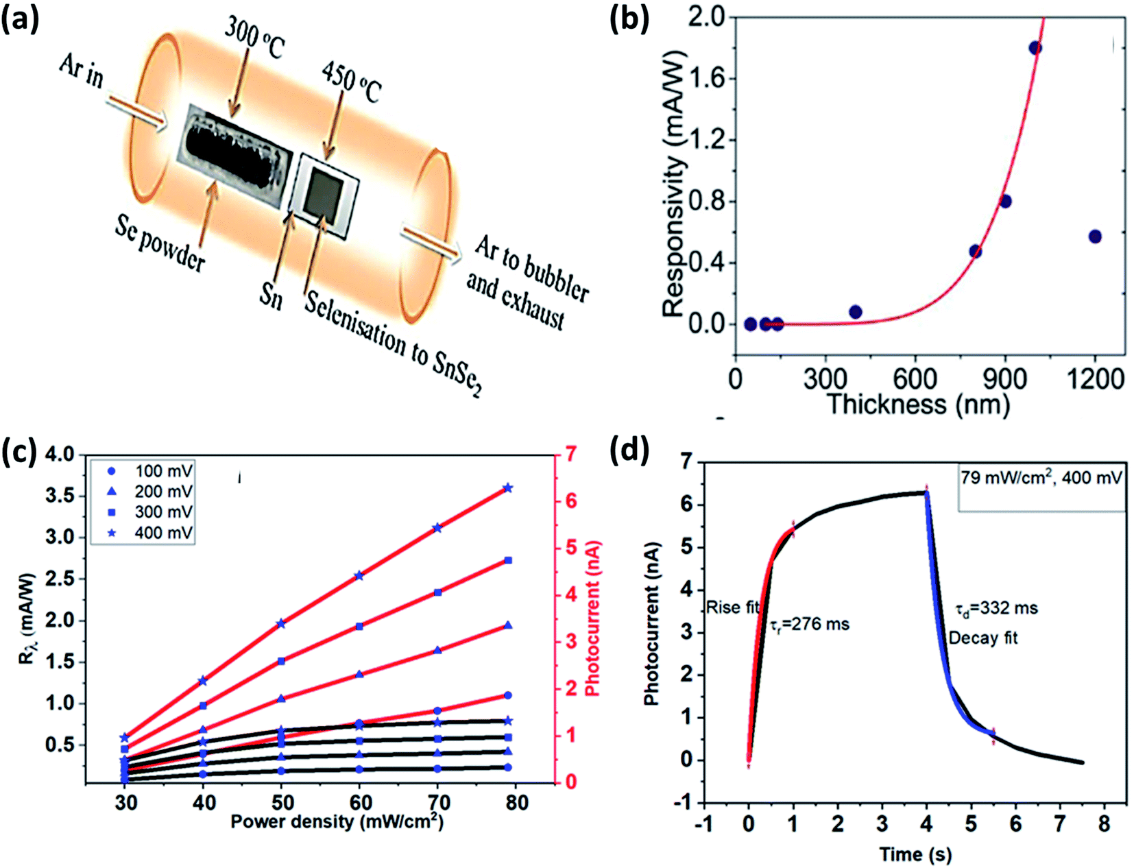 | ||
| Fig. 12 (a) Schematic of selenization of DC sputtered Sn film and (b) thickness-dependent SnSe2 thin films' responsivity. These figures has been adapted/reproduced from ref. 30 with permission from Nature, copyright 2017". (c) Responsivity and photocurrent with power density at different bias voltage and, (d) response and recovery time at 400 mV bias, these figures has been adapted/reproduced from ref. 65 with permission from Elsevier, copyright 2020". | ||
| Device structure | λ (nm) | Bias (V) | R (A W−1) | Detectivity (jones) | Rise/decay time (s) | Ref. |
|---|---|---|---|---|---|---|
| a SED = single exponential decay, DED = double exponential decay. | ||||||
| Ti/Au/Si/SnSe2 (flake)/Ti/Au | 530 | 3 | 1100 | 1010 | 14.5/8.1 × 10−3 | 57 |
| Ti/Au/Si/2LSnSe2/Ti/Au | 633 | 0.1 | 0.5 | — | 2.2/3.2 × 10−3 | 174 |
| Ni/Au/ITO/WSe2 (flake)/SnSe2 (flake)/SiO2/Si/Ni/Au (vertical hetero-structure) | 785 | 0.4 | 1139 | — | 8/32 × 10−6 | 175 |
| Cr/Au/SnSe2 (flake)/MoS2 (flake)/Cr/Au | 500 | 1 | 9.1 × 10³ | 9.3 × 10¹⁰ | 0.2/0.6 | 181 |
| Cr/Au/SLG/SnSe2 (thin film)/Cr/Au | 1064 | 10 | 0.4 × 10⁻³ | 1011 | 2.5/3.68 | 30 |
| Cr/Au/SLG/SnSe2 (thin film)/PEDOT:PSS/Cr/Au | 1064 | 0 | 1.4–2.6 × 10⁻⁶ | ∼108 | 1.33/1.22 | 177 |
| Cr/Au/p-Si/SnSe2/Cr/Au | 1064 | 10 | 0.16 | ∼1.5 × 10⁹ | 57/34 × 10−6 | 182 |
| Au/SLG/SnSe2 (thin film)/Au | 1064 | 0.4 | 0.796 × 10⁻³ | 5.62 × 10⁷ | 0.276/0.332 | 65 |
| Au/Gr/SnSe2 (flake)/Gr/Au | 532 | 0.5 | 1.09 × 10³ | 1.2 × 10¹² | 30.2/27.2 × 10−3 | 183 |
| Ni/Au/SnSe2 (flake)/Ni/Au (suspended structure), Ni/Au/Si/SnSe2 (flake)/Ni/Au (supported structure) | White light | 0.1 | 115, 8.66 × 10⁴ | ∼1013 | SED-66 s, DED-2.27 s, 53 s | 180 |
| Cr/Au/n-Si/SnSe2 (single crystal flake)/Cr/Au | 450 | 3 | 5.11 × 10⁵ | 2.79 × 10¹³ | — | 9 |
4.4 Gas sensors
The gas sensor is a basic need for environment cleaning. A gas sensor is a device, which detects harmful gases and sends an alarm. There are many toxic gases in the environment (CO2, NO2, NH3, SO2, H2S, CH4, etc.). Gas sensing parameters are response time, recovery time, selectivity, gas concentration, temperature, detection limit, etc. Tin based chalcogenide (SnSe and SnSe2) have shown promise for gas sensing applications. A brief discussion of tin chalcogenide (SnSe and SnSe2) materials for gas sensing applications is described. The gas sensing mechanism of the tin chalcogenide (SnSe and SnSe2) gas sensor is based on the adsorption of gas molecule and charge transfer.Physisorption-based charge transfer in tin chalcogenide (SnSe and SnSe2): To evaluate the interaction efficiency of the SnSe/SnSe2 monolayer and gas molecules, the absorption energy (Ea), Hirschfeld charge transfer (Q), and the distance (d0) of nearest atoms between the gas molecule and the SnSe/SnSe2 layer were calculated. The absorbed energy is defined as:
| Ea = Etotal − Egas − Ematerial | (1) |
Egas, Ematerial, and Etotal are the gas molecule's total energy, SnSe/SnSe2 monolayer, and gas molecule-SnSe/SnSe2 system, respectively.184 The adsorption properties, including adsorption energy (Ea), equilibrium distance (d0), and Hirshfeld charge transfer (Q) for SnSe, are listed in Table 6. The adsorbed CO, CO2, CH2O, NO2, and SO2 gas molecules on the β-SnSe monolayer have the Ea values −0.202, −0.175, and −0.322, −0.829, and −0.499 eV, respectively, and the Hirshfeld charge transfer values are −0.033, −0.036, −0.085, −0.279, and −0.279 e, respectively.185
| Molecule | Ea (eV) | d0 (Å) | Q (e) |
|---|---|---|---|
| CO | −0.202 | 3.293 (C–Sn) | −0.033 |
| CO2 | −0.175 | 3.617 (C–Sn) | −0.036 |
| CH2O | −0.322 | 3.222 (H–Sn) | −0.085 |
| O2 | −1.596 | 2.058 (O–Sn) | −0.445 |
| NO2 | −0.829 | 2.531 (O–Sn) | −0.279 |
| SO2 | −0.499 | 2.692 (O–Sn) | −0.279 |
The equilibrium distance of CO, CO2, CH2O, NO2, and SO2 from the β-SnSe layer is 3.293, 3.617, 3.222, 2.531, and 2.692 Å, respectively, which are greater than the C–Sn (2.15 Å), O–Sn (2.22 Å), and N–Sn (2.11 Å) bonds, indicating the process to be physisorption.184 However, the optimized structure shows some distortion for O2 on the surface of the β-SnSe sheet. The value of Ea and Qc for O2 are −1.596 and −0.445 eV, respectively, which is much larger than other gas molecules adsorbed on one SnSe layer, indicating that O2 molecules (CO, CO2, CH2O, NO2, and SO2) are chemically absorbed in the β-SnSe layer.185 Adsorption of CO, CO2, CH2O on the β-SnSe layer showed lower adsorption energy and lower charge transfer values, which indicates that one β-SnSe layer is not suitable for the detection of these three molecules.184
The higher absorption energy of NO2 (−0.829 eV) and SO2 (−0.499 eV) indicates that NO2 and SO2 molecules' absorption behavior for the β-SnSe layer was more potent than that of the absorption system.185 The charge transfer values for NO2 and SO2 are −0.279 and −0.278 eV, respectively, which show a clear charge transfer between the gas molecule and the β-SnSe layer (Fig. 13(a)–(f)).185 The adsorption distances for NO2 and SO2 are 2.531 Å and 2.692 Å, respectively, which is close to the Sn–O bond length range (2.22 Å to 2.66 Å).186 For the β-SnSe sheet, it is crucial to detect NO2 and SO2 in the gas sensor region. All the most stable energy adsorption centers are located on the Sn side of the atom of the β-SnSe sheet, which indicates that the absorbing properties of the metal atom are more substantial than that of the nonmetallic atom.187
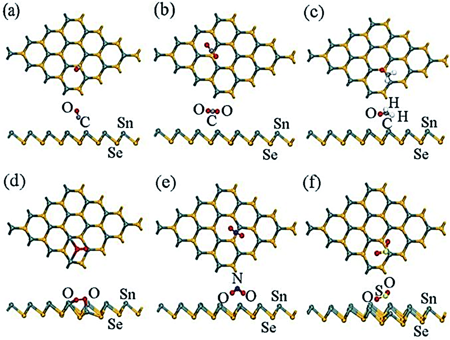 | ||
| Fig. 13 The most stable sites of optimized configurations of the adsorbate molecules: (a) CO, (b) CO2, (c) CH2O, (d) O2, (e) NO2, and (f) SO2 adsorbed on a β-SnSe monolayer. Most stable sites are exhibited. These figures has been adapted/reproduced185 with permission from MDPI, copyright 2019". | ||
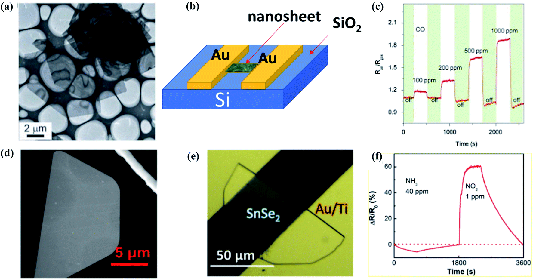 | ||
| Fig. 14 (a) Low magnification TEM images, (b) schematic structure of the device, (c) transient response of the sensor SnO2/SnSe to CO (100–1000 ppm) at 260 μC. These figures has been adapted/reproduced from ref. 191 with permission from Nature, copyright 2013". (d) SEM image of a semi hexagonal nanosheet of SnSe2, (e) optical image of a 6 nm thick SnSe2 gas sensor device, (f) dynamic sensing responses of the 6 nm thick SnSe2 resistor device measured with 405 nm laser illumination. These figures has been adapted/reproduced from ref. 61 with permission from ACS, copyright 2019". | ||
| Material | Structure | Gas | Gas conc. (ppm) | Temp. (°C) | Response | Response time (s) | Recovery time (s) | Ref. |
|---|---|---|---|---|---|---|---|---|
| a R = (Rg − Ra)/Ra × 100.b R = Ra/Rg.c I = (Ig − Io)/Io. R is called the sensor's response, S is called the sensor's sensitivity, Rg is the resistance of the sensor in the presence of target gas, and Ra is the sensor's resistance in the air. Ig is the current of device in presence of target gas and Io is the current of device in presence of air. | ||||||||
| SnSe | Thin film | Methane | 1% vol | 200 | ∼47%a | ∼52 | ∼220 | 21 |
| SnO2/SnSe | Nanosheet | CO | 1000 | 260 | 1.9b | — | — | 191 |
| SnSe2/SnSe | Heterostructure | NO | 1 | RT | 75%c | — | — | 192 |
| p-SnSe/n-SnSe2 | Hetero-structure | NO2 | 0.1 | RT | 30%b | — | — | 193 |
| Material | Structure | Gas | Gas concentration (ppm) | Temp. (°C) | Response | Response time (s) | Recovery time (s) | Ref. |
|---|---|---|---|---|---|---|---|---|
| a S = (Ig − Io)/Io × 100.b R = Ra/Rg.c R = (Ra − Rg)/Rg × 100.d S = (Rg − Ra)/Ra × 100.e R = (Rg/Ra) × 100, where Ig is the current of device in presence of target gas and Io is the current of device in presence of air. R is called the sensor's response, S is called the sensor's sensitivity, Rg is the resistance if the sensor in the presence of target gas, and Ra is the sensor's resistance in the air. | ||||||||
| SnSe2/SnSe | Heterostructure | NO2 | 1 | RT | 75%a | — | — | 192 |
| SnSe2–Ag | Thin film | CO | 500 | 500 | 3.26b | — | — | 197 |
| SnSe2 | Nano plate | Methane | 1% vol | 200 | 66.7c | 78 | 336 | 194 |
| SnSe2 | Pristine monolayer | NO2 | 1 | 50 | 60%b | 142 | 457 | 61 |
| SnSe2 | Thin-film | Methane | 200 | 200 | ∼16%c | ∼75 | ∼615 | 21 |
| p-SnSe/n-SnSe2 | Hetero-structure | NO2 | 0.1 | RT | 30%d | — | — | 193 |
| SnSe2 | Thin film | CH4 | 8000 | 600 | 300%d | — | — | 198 |
| SnSe–SnSe2 | Nanostructured thin film | NO2 | 5 | RT | 112%e | 15 | 10 | 199 |
| Au/Pd/SnSe2 | Thin film | NO2 | 5 | RT | 117%e | 10 | 18.7 | 200 |
4.5 Photocatalysis
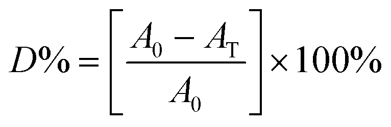 | (2) |
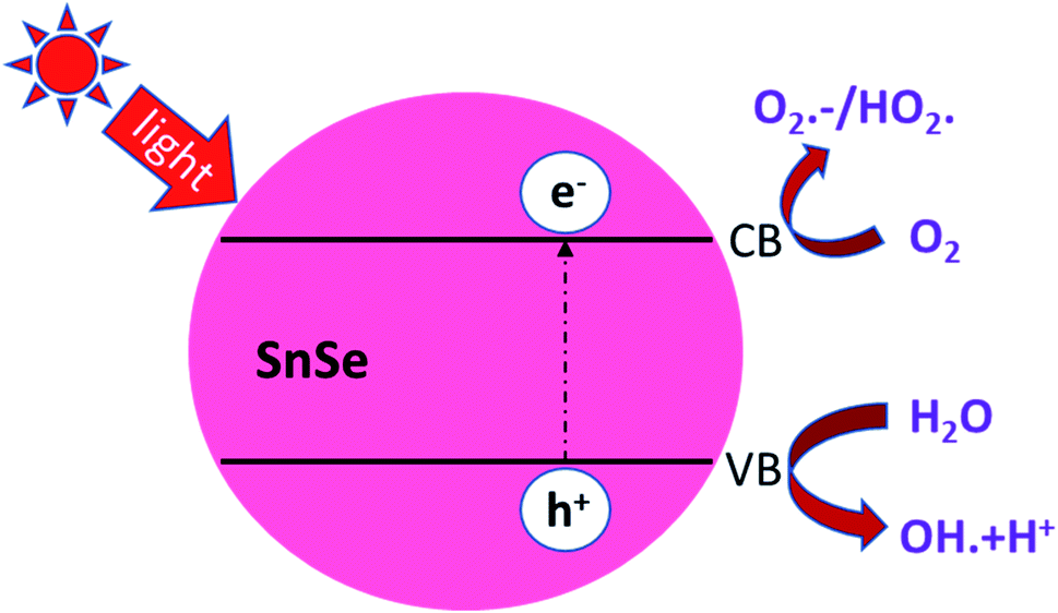 | ||
| Fig. 15 Indicative representation of photodegradation of RhB dye in the presence of UV light. In a typical experiment, the various dyes' degradation rate is checked using eqn (3). These figures has been adapted/reproduced from ref. 62 with permission from Scielo, copyright 2017". | ||
Here A0 is the absorbance of dye in the dark condition. AT is the absorbance of dye at specific time gaps after irradiation of light of a certain wavelength. Li Cheng et al. used the RhB solution under UV radiation to check the SnO2, SnSe, and SnS nano-fibers' photocatalytic activity.62 The degradation curve showed a first-order kinetics equation type curve. The degradation rate for RhB was 85.90%, 92.55% and 92.86% for SnO2, SnS and SnSe, respectively. In another experiment, Jing group used thin films of Sn and SnSe to analyze the photodegradation of RhB.11 Two films SnSe2 and SnSe2/Se were made by the facile solvothermal method. The photocatalytic efficiency was measured from the formula mentioned below,
 | (3) |
The photon falls on the surface, and the elector hole pair is generated. Here, both SnSe and SnO2 took part in the photothermal and photocatalytic processes synchronously. In the process, the electrons from CB of SnSe travels to the CB of SnO2. This increases the oxidation process of photocatalysis and thus improves the photocatalytic behavior. The inner shell SnSe favors the photothermal heat efficiently.201 The photocatalytic activity of SnSe@SnO2 nanocomposite was evaluated through the degradation of methyl orange (MO) experiment under solar light's irradiation. The photocatalytic degradation of MO with SnSe, SnO2, SnSe@SnO2, and P25 (commercially named as TiO2 nanoparticles) was compared using the time versus C/C0 graph. Here, C is the concentration at time t and C0 is the concentration at time t. It was observed that SnSe@SnO2 showed a much higher degradation rate than SnSe, SnO2, and TiO2. In some other methods, blue SE-2R dye degradation was studied by making a composite.
Karamat et al.202 made SnSe composite with LaNdZr2O7 and compared the photocatalytic efficiency with SnSe and blank dye. The setup composed a 300 W Xe arc lamp (PLS-SXE300, Beijing Trusttech Co. Ltd). The degradation of blue dye was analyzed at 658 nm using a UV-Vis spectrophotometer. Before the experiment, the stability of blue dye was checked under dark and light conditions. It was confirmed that the dye was stable, and the continuous illumination does not show any loss in spectra. The photocatalytic degradation experiment was then carried out, and it was found that LaNdZr2O7/SnSe showed a better degradation efficiency. The maximum absorption intensity at wavelength 658 nm showed a decrease in absorption as the irradiation time increases. SnSe alone has demonstrated degradation efficiency of just 15.5% while mixing it with LaNdZr2O7 increased it significantly.
4.6 Storage devices
Zhang et al. synthesized SnSe2 based two-dimensional (2D) nanosheets using the hydrothermal technique. They achieved a theoretical capacity during the first cycle and a stable and reversible specific capacity of 515 mA h g−1 at 0.1 A g−1 after 100 cycles, which exhibited excellent performance.204 The SnSe and SnSe2 both have been used for both sodium and lithium-ion battery applications. Chen et al. (2018) introduced Cu in SnSe for sodium-ion battery and exhibited a capacity of 330 mA h g−1 at 20 A g−1. In a study, Xia et al. used electrospun SnSe with carbon nanofibers for lithium and sodium-ion battery applications and showed improved results. Kim et al. investigated SnSe alloy as an anode for Na-ion batteries. They exhibited excellent electrochemical performance with a high reversible capacity of 707 mA h g−1 and stable performance over 50 cycles.204 In recent time, various studies on SnSe composite has been conducted by multiple research groups to find better results due to the layered structure of SnSe and SnSe2 materials. Table 9 shows a summary of the above discussions.
| Material used | Ion transfer | Cycle rate | Ref. |
|---|---|---|---|
| Cu doped SnSe | Sodium | Retains a capacity of 330 mA h g−1 at 20 A g−1 and 304 mA h g−1 after 1000 cycles at 5 A g−1 (0.1–3.0 V vs. Na/Na+) | 205 |
| Electrospun SnSe/C nanofibers | Lithium and sodium | The discharge capacity of 405 mA h g−1 at 1000 mA g−1 after 500 cycles in lithium-ion battery and 290 mA h g−1 at 200 mA g−1 after 200 cycles in Na+ ion battery | 60 |
| Tin selenide/N-doped carbon composite | Lithium and sodium | For Li ion-discharge capacity 405 mA h g−1 after 500 cycles at a current density of 1000 mA g−1 for Na ion-discharge capacity of 290 mA h g−1 after 200 cycles at 200 mA g−1 | 206 |
| SnSe/SnO2 heterostructure | Lithium | High cyclability having a capacity of 810 mA h g−1 after 200 cycles at a current density value of current density of 400 mA g−1 | 207 |
| Tin diselenide hexagonal nanosheets | Lithium | Specific capacity of 795 mA h g−1 after 100 cycles at 100 mA g−1 | 208 |
| SnSe2 nanoplate–graphene composites | Lithium | Higher storage capacity of 420 mA h g−1 in the first 10 cycles | 55 |
| SnSe2/CNTs hybrid nanostructures | Lithium | SnSe2/CNTs electrode showed specific capacity of 457.6 mA h g−1 at 0.1C and 210.3 mA h g−1 after 100 cycles | 209 |
| SnSe2/reduced graphene oxide (rGO) composite | Sodium | Exhibits an initial efficiency of 73.7%, showing a high capacity of 402.0 mA h g−1 after 150 cycles at 0.1 A g−1 with retention of 86.2% | 210 |
Tin selenide-based composites have shown an excellent theoretical capacity. After many cycles, real practical uses of tin-based anodes in both types of batteries are still very limited. Some structural design, preparation advancement, and morphological development are needed to bring these materials to the production level.
4.7 Memory devices
The phase change from amorphous to crystalline induces a sharp change in the optical and electrical properties like reflectivity and resistivity, respectively. This change in the property is explored to store the data in the form of a bit. As this transition is reversible, this property is utilized in the rewritable data storage. Fast operating speeds, low power consumption, high energy density, large retention time, etc., are the critical parameters for selecting materials for memory applications. Chalcogenides based materials play the central role in this field due to their very short time of the order of few nanoseconds of phase transition, high resistance ratio of the amorphous to the crystalline phase. Chung et al. investigated all phases of the tin selenide (SnSe, SnSe2, Sn2Se3)7 for memory application based on phase change and compared the result with the well-studied GeTe.212 SnSe2 is best among all phases, with high crystallization temperature (220 °C), high electrical contrast (resistance ratio of amorphous to crystalline) of 8.3 × 10⁵, Tg/Tm of 0.52, which showed its potential for the memory application.212 Wang et al. demonstrated the swift recrystallization time of 20 ns for the solution-processed SnSe2 thin film,213 comparable to the commercialize Ge2Sb2Te5. Sun et al. studied the multilayer Si/SnSe2 film by varying the Si's thickness in steps of 4 nm for 0–20 nm, with the film's total thickness nearly constant at 100 nm.214 The varying thickness of the Si did not show any effect on the crystallization temperature. Still, a remarkable change in the resistance of the film with Si thickness of 12 nm {[Si (12 nm)/SnSe2 (5 nm)]6} was observed, i.e., crystalline resistance increased and amorphous resistance decreased, which led to enough (more than three orders of magnitude) electrical contrast to storing information. Simultaneously increasing crystalline resistance reduced the operating current that led to lower power consumption. Multilayer with Si thickness of 12 nm (of nearly 100 nm total thickness) showed its high potential for the low power operated phase-change random access memory (PCRAM) device because of almost ten year retention time at 83 °C and low activation energy.214The difficulty in phase-change memory (PCM) application of these materials is due to high amorphous resistivity of SnSe2, fast crystallization speed, low thermal stability, retention of Sb rich alloy, and very low phase change temperature of Sb. Optimized design of the super lattice like (SLL) structure of SnSe2 and Sb ([SS(10)/S(2)]4) (SS stands for SnSe2 and S for Sb with 10 and 2 nm thickness, respectively) proved to be four times better than the commercialized Ge2Sb2Te5 (GST)215 SLL's resistance with varying temperature and phase switching times for optimized SLL is shown in Fig. 16(a) and (b)). Table 10 shows the comparison of the supremacy of SLL over GST.
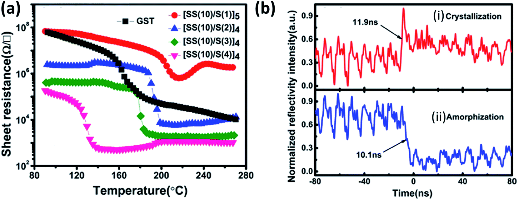 | ||
| Fig. 16 (a) The temperature dependence of resistance for the SLL SS/S and GST thin films at a constant heating rate of 10 °C min−1, and (b) reversible reflectivity evolution of SLL [SS(10)/S(2)] thin film induced by two consecutive picosecond laser pulses with different fluencies: (i) crystallization process and (ii) amorphization process. These figures has been adapted/reproduced from ref. 215 with permission from AIP, copyright 2016". | ||
| Structure | Crystallization temperature (°C) | Crystallization activation energy (eV) | Year data retention at temperature (°C) | Density variation | SET/RESET operation speed (ns) |
|---|---|---|---|---|---|
| Ge2Sb2Te5 | 160 | 2.37 | 10 (75) | 8.2 | 17.7/16.5 |
| [SS(10)/S(2)]4 | 185 | 3.03 | 10 (116) | 3.5 | 11.9/10.1 |
4.8 Topological insulators
Topological insulators are the materials that have insulating bulk accompanied by the protected conducting surface states. These surface states provide an impurity and defect insensitive scattering path to the electrons. The unusual metallic nature of an insulator's surface due to the changes in the insulator's topology is the signature of a topological insulator.216 These surface states are induced due to the high spin–orbit coupling, inverse parity of bulk band, band inversion,217,218 and protected by the time-reversal symmetry.16,218 When the crystal symmetry protects the topological insulator's surface, instead of the time-reversal symmetry protecting it, these insulators are called the topological crystalline insulator (TCI).217 Sun et al.16 reported that SnSe is a TCI in its native phase (without any pressure and alloying) based on the theoretical calculation using the first principle along with ab initio tight-binding modeling. Chen et al.219 reported the co-existence of topological states and superconducting phase at around 27 GPa of the CsCl type phase of SnSe. Ab initio calculation showed that this CsCl phase of SnSe has the topological states' stability against the spin–orbit coupling. SnSe provides the correlation among the superconductivity and topological electronic structures.2195. Conclusion
This review summarizes the tin-selenide material's physical properties, phases, defects, growth mechanisms, deposition methods, and various possible applications. Tin-based compound semiconductors have attracted enormous interest in photovoltaic and optoelectronic applications due to favorable bandgap (1.0–1.3 eV) and higher absorption coefficient (105 cm−1). The reported efficiency of tin selenide based solar cells is very low compared to other compound semiconductor materials like CIGS, CdTe, and CZTSSe. The main limiting factor for tin selenide's relative low efficiency might be defects present in absorber materials, interface trap states, and unfavorable hetero-junction interfaces. Moreover, conduction band offset (CBO) between the absorber and buffer layer plays a crucial role. It needs to be engineered in a precise manner for efficient transport of electrons toward a metal electrode. Thus, fine-tuning of elements, precise control over growth conditions, favorable band alignment between absorber and buffer can pave the way towards improving the power conversion efficiency for realizing the development of environmental-friendly low-cost next-generation photovoltaic technology. Tin selenide can be a potential futuristic material due to its versatile applications. It shows leading hands in some applications in its native crystal structure like thermoelectric. Whereas in other fields it shows competitive nature with the other materials. Tin selenide based thermoelectric materials can pave the ways to reuse waste energy. Tin selenide-based photodetector has also exhibited fast response speed with good responsivity and detectivity in the NIR range.Moreover, flexible photodetector based on tin selenide have also gained attention due to its easy fabrication and fast device response. The device response can be improved by controlling absorber thickness and carrier collection before recombination. Another application based on tin selenide is photocathode in photoelectrochemical water splitting for green hydrogen generation. Lastly, some studies have shown that tin selenide can also be used in gas sensors, storage devices (battery electrode, supercapacitors), memory devices, topological insulators.
Conflicts of interest
Authors declare no conflict of interest exists.Acknowledgements
M. Kumar and Y. Kumar highly acknowledge Council for Scientific and Industrial Research (CSIR), India, and S. Rani acknowledges the University Grant Commission (UGC), India, for grant of Senior Research Fellowship (SRF).References
- A. C. Lokhande, I. A. Qattan, C. D. Lokhande and S. P. Patole, J. Mater. Chem. A, 2020, 8, 918–977 RSC.
- A. C. Lokhande, P. T. Babar, V. C. Karade, M. G. Gang, V. C. Lokhande, C. D. Lokhande and J. H. Kim, J. Mater. Chem. A, 2019, 7, 17118–17182 RSC.
- I. Ali, M. Suhail, Z. A. Alothman and A. Alwarthan, RSC Adv., 2018, 8, 30125–30147 RSC.
- J. Wang, R. Chen, L. Xiang and S. Komarneni, Ceram. Int., 2018, 44, 7357–7377 CrossRef CAS.
- K. M. Chung, D. Wamwangi, M. Woda, M. Wuttig and W. Bensch, J. Appl. Phys., 2008, 103, 083523 CrossRef.
- G. Xing, Y. Li, X. Fan, L. Zhang, W. Zheng and D. J. Singh, J. Appl. Phys., 2017, 121, 225106 CrossRef.
- D. I. Bletskan, J. Ovonic Res., 2005, 1, 61–69 Search PubMed.
- W. Shi, M. Gao, J. Wei, J. Gao, C. Fan, E. Ashalley, H. Li and Z. Wang, Adv. Sci., 2018, 5, 1700602 CrossRef.
- M. Kang, S. Rathi, I. Lee, L. Li, M. A. Khan, D. Lim, Y. Lee, J. Park, A. T. Pham, A. T. Duong, S. Cho, S. J. Yun and G.-H. Kim, J. Nanosci. Nanotechnol., 2017, 18, 4243–4247 CrossRef.
- Z. Li, Y. Guo, F. Zhao, C. Nie, H. Li, J. Shi, X. Liu, J. Jiang and S. Zuo, RSC Adv., 2020, 10, 16749–16755 RSC.
- J. Li, H. Zhao, Y. Lei, Q. Yang and Z. Zheng, Nano, 2018, 13, 1850045 CrossRef CAS.
- K. Chung, D. Wamwangi, M. Woda, M. Wuttig and W. Bensch, J. Appl. Phys., 2008, 103, 083523 CrossRef.
- X. Wang, Y. Liu, J. Dai, Q. Chen, X. Huang and W. Huang, Chem.–Eur. J., 2020, 26, 3870–3876 CrossRef CAS.
- Z. Li, J. Ding and D. Mitlin, Acc. Chem. Res., 2015, 48, 1657–1665 CrossRef CAS.
- B. Pandit, C. D. Jadhav, P. G. Chavan, H. S. Tarkas, J. V. Sali, R. B. Gupta and B. R. Sankapal, IEEE Trans. Power Electron., 2020, 35, 11344–11351 Search PubMed.
- Y. Sun, Z. Zhong, T. Shirakawa, C. Franchini, D. Li, Y. Li, S. Yunoki and X. Q. Chen, Phys. Rev. B: Condens. Matter Mater. Phys., 2013, 88(23), 235122 CrossRef.
- V. E. Drozd, I. O. Nikiforova, V. B. Bogevolnov, A. M. Yafyasov, E. O. Filatova and D. Papazoglou, J. Phys. D: Appl. Phys., 2009, 42(12), 125306 CrossRef.
- Z. Zainal, N. Saravanan, K. Anuar, M. Z. Hussein and W. M. M. Yunus, Mater. Sci. Eng., B, 2004, 107, 181–185 CrossRef.
- M. R. Pallavolu, V. R. Minnam Reddy, P. R. Guddeti and C. Park, J. Mater. Sci.: Mater. Electron., 2019, 30, 15980–15988 CrossRef CAS.
- J. S. Narro-Rios, M. Ramachandran, D. Martínez-Escobar and A. Sánchez-Juarez, J. Semicond., 2013, 34, 013001 CrossRef.
- K. Assili, O. Gonzalez, K. Alouani and X. Vilanova, Arabian J. Chem., 2020, 13, 1229–1246 CrossRef CAS.
- X. Shi, J. Zou and Z. Chen, Chem. Rev., 2020, 120, 7399–7515 CrossRef CAS.
- E. P. Mukhokosi, G. V. S. Manohar, T. Nagao, S. B. Krupanidhi and K. K. Nanda, Micromachines, 2020, 11, 750 CrossRef.
- V. Q. Nguyen, J. Kim and S. Cho, J. Korean Phys. Soc., 2018, 72, 841–857 CrossRef CAS.
- Z. Chen, X. Shi, L. Zhao and J. Zou, Prog. Mater. Sci., 2018, 97, 283–346 CrossRef CAS.
- X.-L. Shi, W.-Y. Chen, X. Tao, J. Zou and Z.-G. Chen, Mater. Horiz., 2020, 7, 3065–3096 RSC.
- B. Qin, W. He and L. D. Zhao, J. Mater., 2020, 6, 671–676 Search PubMed.
- M. Taniguchi, R. L. Johnson, J. Ghijsen and M. Cardona, Phys. Rev. B, 1990, 42, 3634–3643 CrossRef CAS.
- R. E. Abutbul, E. Segev, S. Samuha, L. Zeiri, V. Ezersky, G. Makov and Y. Golan, CrystEngComm, 2016, 18, 1918–1923 RSC.
- E. P. Mukhokosi, S. B. Krupanidhi and K. K. Nanda, Sci. Rep., 2017, 7, 1–10 CrossRef CAS.
- T. Chattopadhyay, J. Pannetier and H. G. Von Schnering, J. Phys. Chem. Solids, 1986, 47, 879–885 CrossRef CAS.
- L. D. Zhao, S. H. Lo, Y. Zhang, H. Sun, G. Tan, C. Uher, C. Wolverton, V. P. Dravid and M. G. Kanatzidis, Nature, 2014, 508, 373–377 CrossRef CAS.
- Y. Ding, B. Xiao, G. Tang and J. Hong, J. Phys. Chem. C, 2017, 121, 225–236 CrossRef CAS.
- M. Zhou, X. Chen, M. Li and A. Du, J. Mater. Chem. C, 2017, 5, 1247–1254 RSC.
- J. M. Gonzalez and I. I. Oleynik, Phys. Rev. B, 2016, 94, 1–10 Search PubMed.
- L. Hao, Z. Wang, H. Xu, K. Yan, S. Dong, H. Liu, Y. Du, Y. Wu, Y. Liu and M. Dong, 2D Mater., 2019, 6(3), 034004 CrossRef CAS.
- G. Xing, Y. Li, X. Fan, L. Zhang, W. Zheng and D. J. Singh, J. Appl. Phys., 2017, 121, 225106 CrossRef.
- L. Chunhong, G. Donglin, K. Li, B. Saho, D. Chen, Y. Ma and J. Sun, Phys. B Phys. Condens. Matter, 2018, 530, 264–269 CrossRef.
- X. Shi, X. Tao, J. Zou and Z. Chen, Adv. Sci., 2020, 7, 1902923 CrossRef CAS.
- Y. Huang, C. Wang, X. Chen, D. Zhou, J. Du, S. Wang and L. Ning, RSC Adv., 2017, 7, 27612–27618 RSC.
- G. Duvjir, T. Min, T. Thi Ly, T. Kim, A. T. Duong, S. Cho, S. H. Rhim, J. Lee and J. Kim, Appl. Phys. Lett., 2017, 110(26), 262106 CrossRef.
- B. B. Nariya, A. K. Dasadia, M. K. Bhayani, A. J. Patel and A. R. Jani, Chalcogenide Lett., 2009, 6, 549–554 CAS.
- G. Shanmugam, U. P. Deshpande, A. Sharma, P. M. Shirage and P. A. Bhobe, J. Phys. Chem. C, 2018, 122, 13182–13192 CrossRef CAS.
- Y. Zhou, W. Li, M. Wu, L. D. Zhao, J. He, S. H. Wei and L. Huang, Phys. Rev. B, 2018, 97(24), 245202 CrossRef CAS.
- L. Song, J. Zhang and B. B. Iversen, J. Mater. Chem. A, 2019, 7, 17981–17986 RSC.
- R. Indirajith, T. P. Srinivasan, K. Ramamurthi and R. Gopalakrishnan, Curr. Appl. Phys., 2010, 10, 1402–1406 CrossRef.
- Y. Gong, C. Chang, W. Wei, J. Liu, W. Xiong, S. Chai, D. Li, J. Zhang and G. Tang, Scr. Mater., 2018, 147, 74–78 CrossRef CAS.
- D. Martínez-Escobar, M. Ramachandran, A. Sánchez-Juárez and J. S. Narro Rios, Thin Solid Films, 2013, 535, 390–393 CrossRef.
- F. Davitt, H. G. Manning, F. Robinson, S. L. Hawken, S. Biswas, N. Petkov, M. van Druenen, J. J. Boland, G. Reid and J. D. Holmes, Adv. Mater. Interfaces, 2020, 7(16), 2000474 CrossRef CAS.
- V. P. Bhatt, K. Gireesan and G. R. Pandya, J. Cryst. Growth, 1989, 96, 649–651 CrossRef CAS.
- A. T. Duong, V. Q. Nguyen, G. Duvjir, V. T. Duong, S. Kwon, J. Y. Song, J. K. Lee, J. E. Lee, S. Park, T. Min, J. Lee, J. Kim and S. Cho, Nat. Commun., 2016, 7(1), 1–6 Search PubMed.
- J. Li, W. Liu, C. Chen, X. Zhao, Z. Qiu, H. Xu, F. Sheng, Q. Hu, Y. Zheng, M. Lin, S. J. Pennycook, C. Su and J. Lu, J. Mater. Chem. A, 2019, 7, 23958–23963 RSC.
- J. Jiang, C. P. Y. Wong, J. Zou, S. Li, Q. Wang, J. Chen, D. Qi, H. Wang, G. Eda, D. H. C. Chua, Y. Shi, W. Zhang and A. T. S. Wee, 2D Mater., 2017, 4(2), 021026 CrossRef.
- Z. Wang, F. Li, J. Guo, C. Ma, Y. Song, Z. He, J. Liu, Y. Zhang, D. Li and H. Zhang, Adv. Opt. Mater., 2020, 8(16), 1902183 CrossRef CAS.
- J. Choi, J. Jin, I. G. Jung, J. M. Kim, H. J. Kim and S. U. Son, Chem. Commun., 2011, 47, 5241–5243 RSC.
- X. Li, L. Li, H. Zhao, S. Ruan, W. Zhang, P. Yan, Z. Sun, H. Liang and K. Tao, Nanomaterials, 2019, 9(9), 1324 CrossRef CAS.
- X. Zhou, L. Gan, W. Tian, Q. Zhang, S. Jin, H. Li, Y. Bando, D. Golberg and T. Zhai, Adv. Mater., 2015, 27(48), 8035–8041 CrossRef CAS.
- D. W. Ma and C. Cheng, J. Nanosci. Nanotechnol., 2013, 13, 4433–4436 CrossRef CAS.
- M. A. Franzman, C. W. Schlenker, M. E. Thompson and R. L. Brutchey, J. Am. Chem. Soc., 2010, 132, 4060–4061 CrossRef CAS.
- J. Xia, Y. Yuan, H. Yan, J. Liu, Y. Zhang, L. Liu, S. Zhang, W. Li, X. Yang, H. Shu, X. Wang and G. Cao, J. Power Sources, 2020, 449, 227559 CrossRef CAS.
- Ó. L. C. Moreira, W. Y. Cheng, H. R. Fuh, W. C. Chien, W. Yan, H. Fei, H. Xu, D. Zhang, Y. Chen, Y. Zhao, Y. Lv, G. Wu, C. Lv, S. K. Arora, C. Ó Coileáin, C. Heng, C. R. Chang and H. C. Wu, ACS Sens., 2019, 4, 2546–2552 CrossRef.
- L. Cheng, D. Li, X. Dong, Q. Ma, W. Yu, X. Wang, H. Yu, J. Wang, G. Liu, L. Cheng, D. Li, X. Dong, Q. Ma, W. Yu, X. Wang, H. Yu, J. Wang and G. Liu, Mater. Res., 2017, 20, 1748–1755 CrossRef CAS.
- C. Zhang, H. Yin, M. Han, Z. Dai, H. Pang, Y. Zheng, Y. Q. Lan, J. Bao and J. Zhu, ACS Nano, 2014, 8, 3761–3770 CrossRef CAS.
- X. Feng, Y. Hu, J. Zhai, C. Wang, S. Song and Z. Song, J. Appl. Phys., 2014, 115, 204303 CrossRef.
- M. Kumar, S. Rani, A. Pandey, K. S. Gour, S. Husale, P. Singh and V. N. Singh, J. Alloys Compd., 2020, 838, 155384 CrossRef CAS.
- M. Powalla, S. Paetel, E. Ahlswede, R. Wuerz, C. D. Wessendorf and T. Magorian Friedlmeier, Appl. Phys. Rev., 2018, 5, 041602 Search PubMed.
- X. Cui, K. Sun, J. Huang, J. S. Yun, C. Y. Lee, C. Yan, H. Sun, Y. Zhang, C. Xue, K. Eder, L. Yang, J. M. Cairney, J. Seidel, N. J. Ekins-Daukes, M. Green, B. Hoex and X. Hao, Energy Environ. Sci., 2019, 12, 2751–2764 RSC.
- X. Li, D. Zhuang, N. Zhang, M. Zhao, X. Yu, P. Liu, Y. Wei and G. Ren, J. Mater. Chem. A, 2019, 7, 9948–9957 RSC.
- D. H. Son, S. H. Kim, S. Y. Kim, Y. I. Kim, J. H. Sim, S. N. Park, D. H. Jeon, D. K. Hwang, S. J. Sung, J. K. Kang, K. J. Yang and D. H. Kim, J. Mater. Chem. A, 2019, 7, 25279–25289 RSC.
- O. P. Singh, K. S. Gour, R. Parmar and V. N. Singh, J. Nanosci. Nanotechnol., 2018, 18, 7670–7681 CrossRef CAS.
- B. Pejjai, V. R. Minnam Reddy, K. Seku, M. R. Pallavolu and C. Park, New J. Chem., 2018, 42, 4843–4853 RSC.
- S. Rühle, Sol. Energy, 2016, 130, 139–147 CrossRef.
- D. V. Shinde, S. K. Min, M. M. Sung, N. K. Shrestha, R. S. Mane and S. H. Han, Mater. Lett., 2014, 115, 244–247 CrossRef CAS.
- N. R. Mathews, Sol. Energy, 2012, 86, 1010–1016 CrossRef CAS.
- J. P. Singh and R. K. Bedi, Jpn. J. Appl. Phys., 1990, 29, L792–L793 CrossRef CAS.
- S. Delice, M. Isik, H. H. Gullu, M. Terlemezoglu, O. Bayrakli Surucu, M. Parlak and N. M. Gasanly, J. Phys. Chem. Solids, 2019, 131, 22–26 CrossRef CAS.
- V. R. Minnam Reddy, G. Lindwall, B. Pejjai, S. Gedi, T. R. R. Kotte, M. Sugiyama, Z. K. Liu and C. Park, Sol. Energy Mater. Sol. Cells, 2018, 176, 251–258 CrossRef CAS.
- M. Nakamura, K. Yamaguchi, Y. Kimoto, Y. Yasaki, T. Kato and H. Sugimoto, IEEE J. Photovoltaics, 2019, 9, 1863–1867 Search PubMed.
- J. Park, H. Yoo, V. Karade, K. S. Gour, E. Choi, M. Kim, X. Hao, S. J. Shin, J. Kim, H. Shim, D. Kim, J. H. Kim, J. Yun and J. hyeok Kim, J. Mater. Chem. A, 2020, 8, 14538–14544 RSC.
- K. S. Gour, R. Parmar, R. Kumar and V. N. Singh, J. Nanosci. Nanotechnol., 2019, 20, 3622–3635 CrossRef.
- M. Dhankhar, O. Pal Singh and V. N. Singh, Renewable Sustainable Energy Rev., 2014, 40, 214–223 CrossRef.
- P. A. Fernandes, M. G. Sousa, P. M. P. Salomé, J. P. Leitão and A. F. Da Cunha, CrystEngComm, 2013, 15, 10278–10286 RSC.
- K. F. Abd El-Rahman, A. A. A. Darwish and E. A. A. El-Shazly, Mater. Sci. Semicond. Process., 2014, 25, 123–129 CrossRef CAS.
- N. E. Makori, I. A. Amatalo, P. M. Karimi and W. K. Njoroge, Int. J. Energy Eng., 2015, 5, 1–4 Search PubMed.
- W. Wang, M. T. Winkler, O. Gunawan, T. Gokmen, T. K. Todorov, Y. Zhu and D. B. Mitzi, Adv. Energy Mater., 2014, 4, 1301465 CrossRef.
- Q. Jin, S. Jiang, Y. Zhao, D. Wang, J. Qiu, D. M. Tang, J. Tan, D. M. Sun, P. X. Hou, X. Q. Chen, K. Tai, N. Gao, C. Liu, H. M. Cheng and X. Jiang, Nat. Mater., 2019, 18, 62–68 CrossRef CAS.
- L. Hu, Y. Zhang, H. Wu, Y. Liu, J. Li, J. He, W. Ao, F. Liu, S. J. Pennycook and X. Zeng, Adv. Funct. Mater., 2018, 28(35), 1803617 CrossRef.
- M. Markov, X. Hu, H. C. Liu, N. Liu, S. J. Poon, K. Esfarjani and M. Zebarjadi, Sci. Rep., 2018, 8, 9876 CrossRef.
- H. Nagai, H. Hamada, K. Hayashi and Y. Miyazaki, J. Electron. Mater., 2019, 48, 1902–1908 CrossRef CAS.
- J. Yang, G. Zhang, G. Yang, C. Wang and Y. X. Wang, J. Alloys Compd., 2015, 644, 615–620 CrossRef CAS.
- G. Shi and E. Kioupakis, J. Appl. Phys., 2015, 117, 065103 CrossRef.
- K. Kutorasinski, B. Wiendlocha, S. Kaprzyk and J. Tobola, Phys. Rev. B: Condens. Matter Mater. Phys., 2015, 91(20), 205201 CrossRef.
- L. Zhao, G. Tan, S. Hao, J. He, Y. Pei, H. Chi, H. Wang, S. Gong, H. Xu, V. P. Dravid, C. Uher, G. J. Snyder, C. Wolverton and M. G. Kanatzidis, Science, 2016, 351(6269), 141–144 CrossRef CAS.
- P. C. Wei, S. Bhattacharya, Y. F. Liu, F. Liu, J. He, Y. H. Tung, C. C. Yang, C. R. Hsing, D. L. Nguyen, C. M. Wei, M. Y. Chou, Y. C. Lai, T. L. Hung, S. Y. Guan, C. S. Chang, H. J. Wu, C. H. Lee, W. H. Li, R. P. Hermann, Y. Y. Chen and A. M. Rao, ACS Omega, 2019, 4(3), 5442–5450 CrossRef CAS.
- M. Jin, Z. Tang, J. Jiang, R. Zhang, L. Zhou, S. Zhao, Y. Chen, Y. Chen, X. Wang and R. Li, Mater. Res. Bull., 2020, 126, 110819 CrossRef CAS.
- C. Chang, M. Wu, D. He, Y. Pei, C. F. Wu, X. Wu, H. Yu, F. Zhu, K. Wang, Y. Chen, L. Huang, J. F. Li, J. He and L. D. Zhao, Science, 2018, 360, 778–783 CrossRef CAS.
- S. Patel, S. H. Chaki and P. C. Vinodkumar, Mater. Res. Express, 2019, 6(8), 085910 CrossRef CAS.
- A. Jayaraman, M. Molli and V. Kamisetti, AIP Conf. Proc., 2015, 1665(1), 110046 CrossRef.
- Y. Tang, L. Shen, Z. Chen, L. Sun, W. Liu, J. Liu and S. Deng, Phys. B Phys. Condens. Matter, 2019, 570, 128–132 CrossRef CAS.
- M. Jin, H. Shao, H. Hu, D. Li, J. Xu, G. Liu, H. Shen, J. Xu, H. Jiang and J. Jiang, J. Cryst. Growth, 2017, 460, 112–116 CrossRef CAS.
- K. Peng, H. Wu, Y. Yan, L. Guo, G. Wang, X. Lu and X. Zhou, J. Mater. Chem. A, 2017, 5, 14053–14060 RSC.
- Y. K. Lee, Z. Luo, S. P. Cho, G. Mercouri, Y. K. Lee, Z. Luo, S. P. Cho, M. G. Kanatzidis and I. Chung, Joule, 2019, 3, 719–731 CrossRef CAS.
- M. Zhang, D. Wang, C. Chang, T. Lin, K. Wang and L. D. Zhao, J. Mater. Chem. C, 2019, 7, 10507–10513 RSC.
- S. Sassi, C. Candolfi, J. Vaney, V. Ohorodniichuk, P. Masschelein, A. Dauscher, B. Lenoir, S. Sassi, C. Candolfi, J. Vaney, V. Ohorodniichuk, P. Masschelein and A. Dauscher, Appl. Phys. Lett., 2014, 104(21), 212105 CrossRef.
- M. Kumar, S. Rani, Y. Singh and V. N. Singh, J. Nanosci. Nanotechnol., 2019, 20, 3636–3646 CrossRef.
- X. Shi, K. Zheng, M. Hong, W. Liu, R. Moshwan, Y. Wang, X. Qu, Z. G. Chen and J. Zou, Chem. Sci., 2018, 9, 7376–7389 RSC.
- L. D. Zhao, C. Chang, G. Tan and M. G. Kanatzidis, Energy Environ. Sci., 2016, 9, 3044–3060 RSC.
- J. Gainza, A. Alonso, N. M. Nemes, J. Gainza, F. Serrano-sa, F. Simon, L. Martı, A. Alonso and N. M. Nemes, Cell reports Phys. Sci., 2020, 1(12), 100263 CrossRef.
- J. Y. Cho, M. Siyar, S. H. Bae, J. S. Mun, M. Y. Kim, S. H. Hong and C. Park, Bull. Mater. Sci., 2020, 43, 63 CrossRef CAS.
- E. K. Chere, Q. Zhang, K. Dahal, F. Cao, J. Mao and Z. Ren, J. Mater. Chem. A, 2016, 4, 1848–1854 RSC.
- Y. X. Chen, Z. H. Ge, M. Yin, D. Feng, X. Q. Huang, W. Zhao and J. He, Adv. Funct. Mater., 2016, 26, 6836–6845 CrossRef CAS.
- X. Shi, A. Wu, T. Feng, K. Zheng, W. Liu, Q. Sun, M. Hong, S. T. Pantelides, Z. G. Chen and J. Zou, Adv. Energy Mater., 2019, 9(11), 1803242 CrossRef.
- C. H. Chien, C. C. Chang, C. L. Chen, C. M. Tseng, Y. R. Wu, M. K. Wu, C. H. Lee and Y. Y. Chen, RSC Adv., 2017, 7, 34300–34306 RSC.
- Y. Luo, S. Cai, X. Hua, H. Chen, Q. Liang, C. Du, Y. Zheng, J. Shen, J. Xu, C. Wolverton, V. P. Dravid, Q. Yan and M. G. Kanatzidis, Adv. Energy Mater., 2019, 9(40), 1901800 CrossRef.
- S. Wang, X. Su, T. P. Bailey, T. Hu, Z. Zhang, G. Tan, Y. Yan, W. Liu, C. Uher and X. Tang, RSC Adv., 2019, 9, 7115–7122 RSC.
- X. Zhang, Y. Wang, G. Zhang, C. Wang and Y. Yan, J. Alloys Compd., 2019, 772, 1061–1066 CrossRef CAS.
- F. Chu, Q. Zhang, Z. Zhou, D. Hou, L. Wang and W. Jiang, J. Alloys Compd., 2018, 741, 756–764 CrossRef CAS.
- W. Lu, S. Li, R. Xu, J. Zhang, D. Li, Z. Feng, Y. Zhang and G. Tang, ACS Appl. Mater. Interfaces, 2019, 11(48), 45133–45141 CrossRef CAS.
- G. Yang, L. Sang, M. Li, S. M. Kazi Nazrul Islam, Z. Yue, L. Liu, J. Li, D. R. G. Mitchell, N. Ye and X. Wang, ACS Appl. Mater. Interfaces, 2020, 12, 12910–12918 CrossRef.
- Q. K. Zhang, S. T. Ning, N. Qi, Z. Q. Chen, X. F. Tang and Z. Y. Chen, J. Appl. Phys., 2019, 125(22), 225109 CrossRef.
- S. Chandra and K. Biswas, J. Am. Chem. Soc., 2019, 141, 6141–6145 CrossRef CAS.
- K. S. Urmila, T. A. Namitha, J. Rajani, R. R. Philip and B. Pradeep, J. Semicond., 2016, 37(9), 093002 CrossRef.
- P. K. Nair, A. K. Martínez, A. R. G. Angelmo, E. B. Salgado and M. T. S. Nair, Semicond. Sci. Technol., 2018, 33(3), 035004 CrossRef.
- C. H. Suen, D. Shi, Y. Su, Z. Zhang, C. H. Chan, X. Tang, Y. Li, K. H. Lam, X. Chen, B. L. Huang, X. Y. Zhou and J. Y. Dai, J. Mater., 2017, 3, 293–298 Search PubMed.
- M. R. Burton, T. Liu, J. Mcgettrick, S. Mehraban, J. Baker, A. Pockett, T. Watson, O. Fenwick and M. J. Carnie, Adv. Mater., 2018, 30(31), 1801357 CrossRef.
- L. Song, J. Zhang and B. B. Iversen, J. Mater. Chem. A, 2019, 7, 17981–17986 RSC.
- Z. Yan, Y. Zhao, D. Liu, Y. Zhang, C. Xue, Z. Zhang, Y. Zheng and J. Cui, RSC Adv., 2020, 10, 43840–43846 RSC.
- P. Wei, S. Bhattacharya, Y.-F. Liu, F. Liu, J. He, Y. Tung, C.-C. Yang, C.-R. Hsing, D.-L. Nguyen, C.-M. Wei, M.-Y. Chou, Y.-C. Lai, T.-L. Hung, S.-Y. Guan, C.-S. Chang, H.-J. Wu, C.-H. Lee, W.-H. Li, R. P. Hermann, Y.-Y. Chen and A. M. Rao, ACS Omega, 2019, 4, 5442–5450 CrossRef CAS.
- S. Sassi, C. Candolfi, J.-B. Vaney, V. Ohorodniichuk, P. Masschelein, A. Dauscher and B. Lenoir, Appl. Phys. Lett., 2014, 104, 212105 CrossRef.
- J. Llorca, D. Cadavid and M. Iba, ACS Appl. Mater. Interfaces, 2020, 12, 27104–27111 CrossRef.
- S. Chandra, P. Dutta and K. Biswas, ACS Appl. Energy Mater., 2020, 3, 9051–9057 CrossRef CAS.
- B. Cai, H. L. Zhuang, H. Tang and J. F. Li, Nano Energy, 2019, 104393 Search PubMed.
- J. Cha, C. Zhou, Y. K. Lee, S. P. Cho and I. Chung, ACS Appl. Mater. Interfaces, 2019, 11, 21645–21654 CrossRef CAS.
- Y. K. Lee, Z. Luo, S. P. Cho, M. G. Kanatzidis and I. Chung, Joule, 2019, 3, 719–731 CrossRef CAS.
- C. Ho, W. Lin, L. Chao, K. Lee, J. Inagaki and H. Hsueh, ACS Appl. Energy Mater., 2020, 3(5), 4896–4905 CrossRef CAS.
- Y. Zhong, L. Zhang, V. Linseis, B. Qin, W. Chen, L. Zhao and H. Zhu, Nano Energy, 2020, 72, 104742 CrossRef CAS.
- B. Z. Sun, Z. Ma, C. He and K. Wu, Phys. Chem. Chem. Phys., 2015, 17, 29844–29853 RSC.
- S. Saha, A. Banik and K. Biswas, Chem.–Eur. J., 2016, 22, 15634–15638 CrossRef CAS.
- P. Xu, T. Fu, J. Xin, Y. Liu, P. Ying, X. Zhao, H. Pan and T. Zhu, Sci. Bull., 2017, 62, 1663–1668 CrossRef CAS.
- Y. Luo, Y. Zheng, Z. Luo, S. Hao, C. Du, Q. Liang, Z. Li, K. A. Khor, K. Hippalgaonkar, J. Xu, Q. Yan, C. Wolverton and M. G. Kanatzidis, Adv. Energy Mater., 2018, 8, 2–7 Search PubMed.
- F. Li, Z. Zheng, Y. Li, W. Wang, J. F. Li, B. Li, A. Zhong, J. Luo and P. Fan, J. Mater. Sci., 2017, 52, 10506–10516 CrossRef CAS.
- Y. Wu, W. Li, A. Faghaninia, Z. Chen, J. Li, X. Zhang, B. Gao, S. Lin, B. Zhou, A. Jain and Y. Pei, Mater. Today Phys., 2017, 3, 127–136 CrossRef.
- Y. Shu, X. Su, H. Xie, G. Zheng, W. Liu, Y. Yan, T. Luo, X. Yang, D. Yang, C. Uher and X. Tang, ACS Appl. Mater. Interfaces, 2018, 10, 15793–15802 CrossRef CAS.
- C. Liu, Z. Huang, D. Wang, X. Wang, L. Miao, X. Wang, S. Wu, N. Toyama, T. Asaka, J. Chen, E. Nishibori and L.-D. Zhao, J. Mater. Chem. A, 2019, 7(16), 9761–9772 RSC.
- J. Wang, X. Jia, S. Lou, G. Li and S. Zhou, ACS Omega, 2020, 5(21), 12409–12414 CrossRef CAS.
- D. Yin, Y. Liu, C. Dun, D. L. Carroll and M. T. Swihart, Nanoscale, 2018, 10, 2533–2541 RSC.
- J. Chen, D. M. Hamann, D. Choi, N. Poudel, L. Shen, L. Shi, D. C. Johnson and S. Cronin, Nano Lett., 2018, 18, 6876–6881 CrossRef CAS.
- A. T. Duong, D. L. Nguyen, M. N. Nguyen, T. M. H. Nguyen, A. D. Nguyen, A. T. Pham, F. Ullah, Z. Tahir, Y. S. Kim, D. Q. Trung, T. Nguyen, H. Van Bui, R. Das, P. T. Huy and S. Cho, Mater. Res. Express, 2019, 6, 066420 CrossRef CAS.
- X. Zhang, D. Liu, L. Yang, L. Zhou and T. You, J. Mater. Chem. A, 2015, 3, 10031–10037 RSC.
- Y. Li, B. He, J. P. Heremans, J. Zhao, B. He and J. P. Heremans, J. Alloys Compd., 2016, 669, 224–231 CrossRef CAS.
- D. Ibrahim, J. Vaney, S. Sassi, C. Candolfi, V. Ohorodniichuk, P. Levinsky, C. Semprimoschnig, A. Dauscher and B. Lenoir, Appl. Phys. Lett., 2017, 110, 032103 CrossRef.
- P. C. Wei, S. Bhattacharya, J. He, S. Neeleshwar, R. Podila, Y. Y. Chen and A. M. Rao, Nature, 2016, 539, E1–E2 CrossRef CAS.
- R. Gupta and C. Bera, Nano Express, 2020, 1, 030035 CrossRef.
- N. E. Makori, I. A. Amatalo, P. M. Karimi and W. K. Njoroge, Am. J. Condens. Matter Phys., 2014, 4, 87–90 Search PubMed.
- N. Ghobadi and E. Gholami Hatam, Opt. Quantum Electron., 2019, 51(8), 269 CrossRef.
- A. S. Pawbake, S. R. Jadkar and D. J. Late, Mater. Res. Express, 2016, 3, 105038 CrossRef.
- L. Hao, H. Xu, S. Dong, Y. Du, L. Luo, C. Zhang, H. Liu, Y. Wu and Y. Liu, IEEE Electron Device Lett., 2018, 40(1), 55–58 Search PubMed.
- J. Yao, Z. Zheng and G. Yang, Adv. Funct. Mater., 2017, 27, 1701823 CrossRef.
- J. Liu, Q. Huang, K. Zhang, Y. Xu, M. Guo, Y. Qian, Z. Huang, F. Lai and L. Lin, Nanoscale Res. Lett., 2017, 12, 259 CrossRef.
- H. Yao, S. Luo, G. S. Duesberg, X. Qi, D. Lu, C. Yue and J. Zhong, AIP Adv., 2018, 8, 075123 CrossRef.
- Y. Zhong, L. Zhang, M. Sun, M. Wang, W. Chen, S. Lin, D. Xie and H. Zhu, Mater. Today Energy, 2019, 12, 418–425 CrossRef.
- L. Hao, Y. Du, Z. Wang, Y. Wu, H. Xu, S. Dong, H. Liu, Y. Liu, Q. Xue, Z. Han, K. Yan and M. Dong, Nanoscale, 2020, 12, 7358–7365 RSC.
- B. Ouyang, C. Chang, L. Zhao, Z. Lin and Y. Yang, Nano Energy, 2019, 66, 104111 CrossRef CAS.
- D. Zheng, H. Fang, M. Long, F. Wu, P. Wang, F. Gong, X. Wu, J. C. Ho, L. Liao and W. Hu, ACS Nano, 2018, 12, 7239–7245 CrossRef CAS.
- A. S. Pawbake, S. R. Jadkar and D. J. Late, Mater. Res. Express, 2016, 3, 105038 CrossRef.
- J. Yao, Z. Zheng and G. Yang, Adv. Funct. Mater., 2017, 27, 1701823 CrossRef.
- L. Hao, Z. Wang, H. Xu, K. Yan, S. Dong, H. Liu, Y. Du, Y. Wu, Y. Liu and M. Dong, 2D Mater, 2019, 6, 034004 CrossRef CAS.
- L. Hao, Y. Du, Z. Wang, Y. Wu, H. Xu, S. Dong, H. Liu, Y. Liu, Q. Xue, Z. Han, K. Yan and M. Dong, Nanoscale, 2020, 12, 7358–7365 RSC.
- X.-Z. Li, Y.-F. Wang, J. Xia and X.-M. Meng, Nanoscale Adv., 2019, 1, 2606–2611 RSC.
- Z. Jia, J. Xiang, F. Wen, R. Yang, C. Hao and Z. Liu, ACS Appl. Mater. Interfaces, 2016, 8(7), 4781–4788 CrossRef CAS.
- K. Patel, P. Chauhan, A. B. Patel, G. K. Solanki, K. D. Patel and V. M. Pathak, ACS Appl. Nano Mater., 2020, 3(11), 11143–11151 CrossRef CAS.
- H. Xu, L. Hao, H. Liu, S. Dong, Y. Wu, Y. Liu, B. Cao, Z. Wang, C. Ling, S. Li, Z. Xu, Q. Xue and K. Yan, ACS Appl. Mater. Interfaces, 2020, 12, 35250–35258 CrossRef CAS.
- X. Zhou, L. Gan, W. Tian, Q. Zhang, S. Jin, H. Li, Y. Bando, D. Golberg and T. Zhai, Adv. Mater., 2015, 27, 8035–8041 CrossRef CAS.
- P. Yu, X. Yu, W. Lu, H. Lin, L. Sun, K. Du, F. Liu, W. Fu, Q. Zeng, Z. Shen, C. Jin, Q. J. Wang and Z. Liu, Adv. Funct. Mater., 2016, 26, 137–145 CrossRef CAS.
- K. Murali and K. Majumdar, IEEE Trans. Electron Devices, 2018, 65, 4141–4148 CAS.
- X. Zhou, N. Zhou, C. Li, H. Song, Q. Zhang, X. Hu, L. Gan, H. Li, J. Lü, J. Luo, J. Xiong and T. Zhai, 2D Mater, 2017, 4, 025048 CrossRef.
- E. P. Mukhokosi, S. B. Krupanidhi and K. K. Nanda, Phys. Status Solidi A, 2018, 215, 1800470 CrossRef.
- E. P. Mukhokosi, B. Roul, S. B. Krupanidhi and K. K. Nanda, ACS Appl. Mater. Interfaces, 2019, 11, 6184–6194 CrossRef CAS.
- W. Gao, Z. Zheng, Y. Li, Y. Zhao, L. Xu, H. Deng and J. Li, Nanoscale, 2019, 11, 13309–13317 RSC.
- M. Krishna, S. Kallatt and K. Majumdar, Nanotechnology, 2018, 29, 035205 CrossRef.
- X. Zhou, N. Zhou, C. Li, H. Song, Q. Zhang, X. Hu, L. Gan, H. Li, J. Lü, J. Luo, J. Xiong and T. Zhai, 2D Mater., 2017, 4, 025048 CrossRef.
- E. P. Mukhokosi, B. Roul, S. B. Krupanidhi and K. K. Nanda, ACS Appl. Mater. Interfaces, 2019, 11, 6184–6194 CrossRef CAS.
- W. Gao, Z. Zheng, Y. Li, Y. Zhao, L. Xu, H. Deng and J. Li, Nanoscale, 2019, 11, 13309–13317 RSC.
- J. Wang, G. F. Yang, J. J. Xue, J. M. Lei, D. J. Chen, H. Lu, R. Zhang and Y. D. Zheng, IEEE Electron Device Lett., 2018, 39, 599–602 CAS.
- T. Liu, H. Qin, D. Yang and G. Zhang, Coatings, 2019, 9(6), 390 CrossRef CAS.
- I. D. Brown, J. Solid State Chem., 1974, 11, 214–233 CrossRef CAS.
- C. Feng, H. Qin, D. Yang and G. Zhang, Materials, 2019, 12(4), 676 CrossRef CAS.
- X. He, H. Shen, W. Wang, Z. Wang, B. Zhang and X. Li, J. Alloys Compd., 2013, 556, 86–93 CrossRef CAS.
- G. Shi and E. Kioupakis, Nano Lett., 2015, 15, 6926–6931 CrossRef.
- I. Lefebvre, M. A. Szymanski, J. Olivier-Fourcade and J. C. Jumas, Phys. Rev. B, 1998, 58, 1896–1906 CrossRef CAS.
- J.-J. Wang, A.-F. Lv, Y.-Q. Wang, B. Cui, H.-J. Yan, J.-S. Hu, W.-P. Hu, Y.-G. Guo and L.-J. Wan, Sci. Rep., 2013, 3(1), 2613 CrossRef.
- L. Lee, C. W. Chen, A. Manikandan, S. H. Lee, Z. M. Wang and Y. L. Chueh, Nano Energy, 2018, 44, 419–429 CrossRef.
- X. Wang, Y. Liu, J. Dai, Q. Chen, X. Huang and W. Huang, Chem.–Eur. J., 2020, 26, 3870–3876 CrossRef CAS.
- M. Chen, Z. Li, W. Li, C. Shan, W. Li, K. Li, G. Gu, Y. Feng, G. Zhong, L. Wei and C. Yang, Nanotechnology, 2018, 29(45), 455501 CrossRef.
- B. Subramanian, T. Mahalingam, C. Sanjeeviraja, M. Jayachandran and M. J. Chockalingam, Thin Solid Films, 1999, 357, 119–124 CrossRef CAS.
- S. J. Choi and I. D. Kim, Recent Developments in 2D Nanomaterials for Chemiresistive-Type Gas Sensors Electronic Mater. Lett., 2018, 14(3), 221–260 CAS.
- M. Popescu, A. Velea, F. Sava, A. Lőrinczi, A. Tomescu, C. Simion, E. Matei, G. Socol, I. N. Mihailescu, A. Andonie and I. Stamatin, Phys. Status Solidi, 2010, 207, 516–520 CrossRef CAS.
- M. Popescu, F. Sava, A. Lorinczi, G. Socol, I. N. Mihǎilescu, A. Tomescu and C. Simion, J. Non-Cryst. Solids, 2007, 353, 1865–1869 CrossRef CAS.
- S. Rani, M. Kumar, Y. Singh, M. Tomar, A. Sharma, V. Gupta and V. N. Singh, J. Nanosci. Nanotechnol., 2021, 11 DOI:10.1166/jnn.2021.19278.
- S. Rani, M. Kumar, Y. Singh and V. N. Singh, J. Nanosci. Nanotechnol., 2021, 11 DOI:10.1166/jnn.2021.19277.
- Z. Li, L. Sun, Y. Liu, D. Yu, Y. Wang, Y. Sun and M. Yu, Environ. Sci. Nano, 2019, 6, 1507–1515 RSC.
- M. Karamat, M. Fahad Ehsan, M. Naeem Ashiq, S. Ijaz, M. Najam-ul-Haq, S. Hamid and H.N. Bahnemann, Appl. Surf. Sci., 2019, 463, 1019–1027 CrossRef.
- F. Zhang, C. Xia, J. Zhu, B. Ahmed, H. Liang, D. B. Velusamy, U. Schwingenschlögl and H. N. Alshareef, Adv. Energy Mater., 2016, 6, 1601188 CrossRef.
- Y. Kim, Y. Kim, Y. Park, Y. N. Jo, Y. J. Kim, N. S. Choi and K. T. Lee, Chem. Commun., 2015, 51, 50–53 RSC.
- R. Chen, S. Li, J. Liu, Y. Li, F. Ma, J. Liang, X. Chen, Z. Miao, J. Han, T. Wang and Q. Li, Electrochim. Acta, 2018, 282, 973–980 CrossRef CAS.
- N. Shaji, P. Santhoshkumar, H. S. Kang, M. Nanthagopal, J. W. Park, S. Praveen, G. S. Sim, C. Senthil and C. W. Lee, J. Alloys Compd., 2020, 834, 154304 CrossRef CAS.
- K. Chen, X. Wang, G. Wang, B. Wang, X. Liu, J. Bai and H. Wang, Chem. Eng. J., 2018, 347, 552–562 CrossRef CAS.
- Q. Yu, B. Wang, J. Wang, S. Hu, J. Hu and Y. Li, Front. Chem., 2020, 8, 590 CrossRef CAS.
- H. Chen, B.-E. Jia, X. Lu, Y. Guo, R. Hu, R. Khatoon, L. Jiao, J. Leng, L. Zhang and J. Lu, Chem.–Eur. J., 2019, 25, 9973–9983 CrossRef CAS.
- T. Wang, K. Yang, J. Shi, S. Zhou, L. Mi, H. Li and W. Chen, J. Energy Chem., 2020, 46, 71–77 CrossRef.
- D. Ni, Y. Chen, X. Yang, C. Liu and K. Cai, J. Alloys Compd., 2018, 737, 623–629 CrossRef CAS.
- K. M. Chung, D. Wamwangi, M. Woda, M. Wuttig and W. Bensch, J. Appl. Phys., 2008, 103(8), 083523 CrossRef.
- R. Y. Wang, M. A. Caldwell, R. Gnana, D. Jeyasingh, S. Aloni, R. M. Shelby, R. Y. Wang, M. A. Caldwell, R. Gnana, D. Jeyasingh, S. Aloni, R. M. Shelby, H. P. Wong and D. J. Milliron, J. Appl. Phys., 2011, 109(11), 113506 CrossRef.
- A. I. Journal, M. Sun, Y. Hu, B. Shen, J. Zhai and S. Song, Integr. Ferroelectr., 2012, 140(1), 1–7 CrossRef.
- W. Wu, Z. He, S. Chen, J. Zhai, X. Liu, T. Lai, S. Song and Z. Song, J. Appl. Phys., 2016, 120(16), 165106 CrossRef.
- J. E. Moore, Nature, 2010, 464, 194–198 CrossRef CAS.
- J. Shen and J. J. Cha, Nanoscale, 2014, 6, 14133–14140 RSC.
- L. Müchler, H. Zhang, S. Chadov, B. Yan, F. Casper, J. Kübler, S. C. Zhang and C. Felser, Angew. Chem., Int. Ed., 2012, 51, 7221–7225 CrossRef.
- X. Chen, P. Lu, X. Wang, Y. Zhou, C. An, Y. Zhou, C. Xian, H. Gao, Z. Guo, C. Park, B. Hou, K. Peng, X. Zhou, J. Sun, Y. Xiong, Z. Yang, D. Xing and Y. Zhang, Phys. Rev. B, 2017, 96, 165123 CrossRef.
| This journal is © The Royal Society of Chemistry 2021 |