
 Open Access Article
 This Open Access Article is licensed under a Creative Commons Attribution-Non Commercial 3.0 Unported Licence
Manipulating the Raman scattering rotation via magnetic field in an MoS2 monolayer†
Yi Wan‡
 *ab,
Xing Cheng‡bc,
Yanfang Lid,
Yaqian Wangd,
Yongping Dua,
Yibin Zhaoa,
Bo Pengd,
Lun Dai*bc and
Erjun Kan*a
*ab,
Xing Cheng‡bc,
Yanfang Lid,
Yaqian Wangd,
Yongping Dua,
Yibin Zhaoa,
Bo Pengd,
Lun Dai*bc and
Erjun Kan*a
aDepartment of Applied Physics and Institution of Energy and Microstructure, Nanjing University of Science and Technology, Nanjing 210094, China. E-mail: wany@njust.edu.cn; ekan@njust.edu.cn
bState Key Laboratory for Artificial Microstructure & Mesoscopic Physics, School of Physics, Peking University, Beijing 100871, China. E-mail: lundai@pku.edu.cn
cCollaborative Innovation Center of Quantum Matter, Beijing 100871, China
dNational Engineering Research Center of Electromagnetic Radiation Control Materials and State Key Laboratory of Electronic Thin Films and Integrated Devices, School of Microelectronics and Solid State Electronics, University of Electronic Science and Technology of China, Chengdu 610054, China
First published on 20th January 2021
Abstract
Magneto-optical effects, which originate from the interactions between light and magnetism, have provided an important way to characterize magnetic materials and hosted abundant applications, such as light modulators, magnetic field sensors, and high-density data storage. However, such effects are too weak to be detected in non-magnetic materials due to the absence of spin degree of freedom. Here, we demonstrated that applying a perpendicular magnetic field can produce a colossal Raman scattering rotation in non-magnetic MoS2, for A-mode representing the out-of-plane breathing vibration. Our experimental results show that linearly polarized scattering light is rotated by ∓125°, more apparent than the valley Zeeman splitting effect (∓1.2 meV) under the same experimental conditions (±5 T), near room temperature. A detailed and systematic analysis on the polarization-resolved magnetic field-dependent micro-zone Raman intensity offers a feasible way to manipulate the inelastically scattered light via a magnetic technique. This explored phenomenology and physical mechanism arouse a new ramification of probing burgeoning magneto-optical effects in the field of two-dimensional laminar materials.
Introduction
Two-dimensional (2D) materials have received considerable attention and interest since the successful isolation of graphene for the first time.1 In recent years, transition metal dichalcogenides (TMDCs) have become the flagship materials after graphene. The considerable extraordinary properties of TMDCs include the direct bandgap in visible and near-infrared wavelengths, suitable for exploring their potential in optoelectronics,2 and the fascinating mechanism concerning the spin and the valley pseudospin, enabling unprecedented electronic devices or techniques.3 However, due to the limited thickness of such van der Waals (vdWs) materials, particularly for the monolayer, it is difficult to characterize the intrinsic properties experimentally, which is inappropriate to the rapid development in this field.Raman spectroscopy primarily focuses on the measurement of the inelastic scattering radiation generated from collective quasi-particle excitations.4 The crystal structure, atomic vibrating mode, and polarization angles between the incident light and detected light all have significant impacts on the intensity of Raman modes, making it an exceedingly effective technique for studying the crystal property and the property variation attributed from external perturbations. As reported in literature, Raman spectroscopy has been performed to examine the changes in the material property influenced by temperature,5,6 humidity,7 strain,8 externally applied electric field,9 or magnetic field.10,11 Along with the research upsurge in 2D magnets, Raman spectroscopy12–17 has been broadly adopted to characterize the magnetic property based on the surface sensitivity and remarkable magneto-optical effects. The successful applications of inelastic light scattering in such magnets has provided important information in studying magnetic impurity light scattering,18,19 defect magnetism,20 spin-flip inelastically scattered light in diluted magnetic semiconductors,21,22 and lattice vibrations in colossal magneto-resistive materials.23–25 However, in most of the fabricated 2D vdWs materials, the absence of spin moments can only provide limited electronic or structural information relying solely on Raman techniques.
Molybdenum disulfide (MoS2), a representative 2D semiconductor in the TMDC family, has recently drawn extensive attention.26 In laminar MoS2, the bulk crystals are formed by stacking covalently-bonded S–Mo–S sandwiched trilayers via relatively weak vdWs interactions. As the thickness is thinned from bulk to monolayer, on account of the 2D quantum confinement effect, the bandgap of MoS2 will transfer from indirect to direct, with remarkable increase in the luminescence quantum efficiency.26,27 Briefly, with the distinct crystal structure enabling the degenerate-but-inequivalent valleys,28–30 remarkable photoluminescence (PL) in the visible frequency range26,27 and appropriate Gibbs free energy for large-scale hydrogen production applications,31,32 monolayer MoS2 has offered considerable potential for the exploration of excellent electronic33,34 and optoelectronic35–37 devices. Herein, by performing polarization-resolved magneto-Raman spectroscopy measurements, we discovered a gigantic scattering rotation of A-mode in the Raman spectra obtained from MoS2 monolayers in the presence of a perpendicular magnetic field. Although the well-known valley Zeeman splitting under the same conditions is quite weak as expected, the maximum Raman scattering feature rotation is about ∓125°, which has never been observed. This obvious magneto-optical effect originates from the symmetry breaking when the magnetic field is perpendicularly applied, particularly for the electron motion during the inelastically scattering process, which implies that the non-magnetic laminar materials can still exhibit an apparent response to the magnetic field. Thus, our study validates the magneto-Raman spectroscopy as a sensitive technique to characterize properties in quantum material systems, refines the microscopic inelastic scattering theory and demonstrates new avenues for modulating the optical signals based on the phonon polarity-related symmetry, providing a platform for the innovative magneto-optical devices and techniques based on 2D laminar materials, such as phonon lasers and nanomechanical oscillators.
Results and discussion
MoS2 samples were synthesized directly on the surface of Si/SiO2 substrates via the commonly used chemical vapor deposition (CVD) method.38,39 From the optical microscopy image (Fig. 1a) and the atomic force microscope (AFM) topography image (Fig. 1b), we can see that most MoS2 domains on Si/SiO2 appear as triangles with the side length of 28.1 ± 12.8 μm (ESI Fig. S1†), obeying the symmetry of the hexagonal crystal lattice. The height profile along the MoS2 triangular domain shows a terrace of ∼0.66 nm, as an indication of the monolayer. When imaged at a higher resolution, as shown in the lateral deflection signal obtained by AFM (Fig. 1c), the MoS2 lattice possessing a honeycomb-like hexagonal arrangement of spots can be clearly resolved. This high-resolution AFM image was obtained via a conventional tip (TR400PSA) operating at ambient conditions, readily shown in the AFM lateral deflection images but only occasionally in the AFM topography images. It should be mentioned that the lattice-resolution image does not exhibit the accurate atomic-level resolution; on the contrary, the actual contact area between the scanned-cantilever and the MoS2 sample surface is up to the order of 10 × 10 nm2; however, the periodic stick-slip atomic-level frictional forces are adequate to capture the lattice-level resolution, sufficiently enough to determine the crystallographic orientation.40,41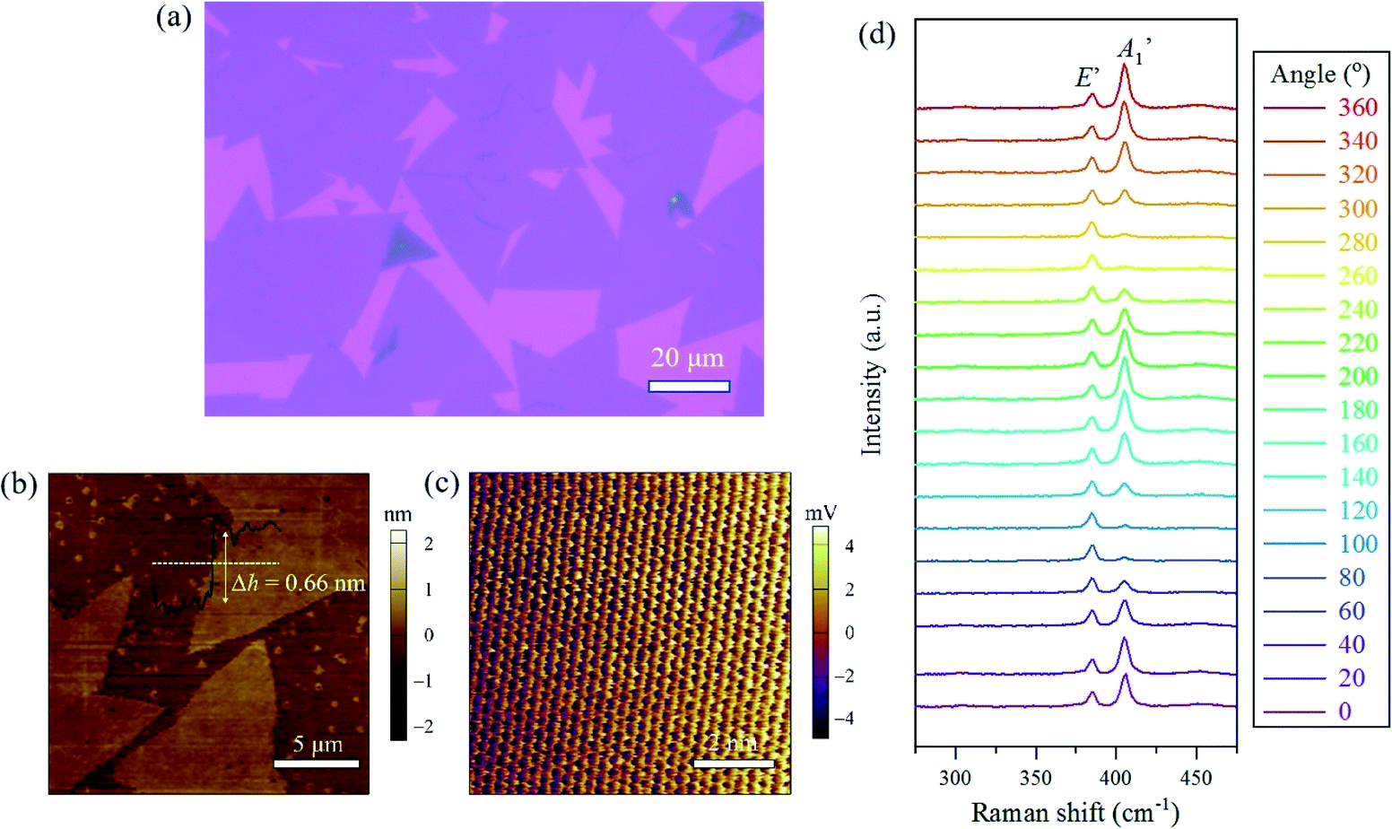 | ||
| Fig. 1 (a) Optical microscopy image of the MoS2 monolayers synthesized on the Si/SiO2 substrate. (b) AFM topography image of MoS2 monolayers synthesized on the Si/SiO2 substrate, together with the corresponding height analysis. (c) Magnified AFM lateral deflection image of MoS2, exhibiting the hexagonal lattice structure. (d) A series of Raman spectra of the MoS2 monolayer, along with the polarization angles between the incident light and the scattered radiation. | ||
Bulk MoS2 belongs to the space group of D6h, possessing a dozen of vibration modes at the high-symmetric Γ point,8 four of which are first-order active, named in terms of the vibration mode symmetry, as E22g, E1g, E12g, and A1g. The E1g mode is forbidden, while E12g and A1g modes are allowed when the incident excitation light propagates along the MoS2 c-axis as the light path configuration used in our experiments. The low-wavenumber E22g mode is not in view in this study. For the MoS2 monolayer, the A- and E-mode symmetries will become  and E′. Besides, the monolayer nature of MoS2 samples can be easily identified by distinguishing the peak position interval between the
  and E′ modes, which is prevailingly adopted to determine the thickness of ultrathin MoS2 nanoflakes42 and confirmed by PL spectrum as a supplement.26,27 As a direct-gap semiconductor, the PL spectrum of the MoS2 monolayer on Si/SiO2 exhibits a strong excitonic emission (ESI, Fig. S2†).
The schematic of the experimental set-up for micro-zone Raman signal collection under the magnetic fields is shown in Fig. 2a. From the top view, the linear polarizer in front of the notch filter enables the collection of the polarization-resolved optical signal. During the process of signal collection, we began along the parallel direction (φ = 0°) and continuously rotated the polarizer with the step of 10° until a cycle of 360° was finished. For compactness and simplicity, only 19 measured Raman spectra, along with the polarization angles between the incident light and the scattered radiation with the step of 20° are plotted in Fig. 1d. Two dominant peaks at 384 and 404 cm−1, corresponding to the E′ and  modes, are clearly observed. As shown in this series of Raman spectra (Fig. 1d), the breathing mode along the c-axis of S atoms
  exhibits a noteworthy polar dependence and can be negligible when the polarization angle reaches 90°, where the polarized incident light and the scattered light are orthogonal. In comparison, the intensities of the in-plane shearing motion (E′) vary very slightly. The polar behavior of these two modes, regardless of the MoS2 crystalline orientation, only shows the relationship with the polarization angles between the incident and scattered lights when no magnetic field is applied (ESI, Fig. S3†), which can be easily understood by the optical selection rules based on the symmetry of MoS2 Raman tensors (more discussion later).8
 | ||
| Fig. 2 (a) A schematic of the experimental set-up for micro-zone magneto-Raman measurements. Positive magnetic field is defined as the upward direction. The excitation laser is a 532 nm continuous wave (CW) laser. (b) Polarization-dependence of Raman spectra corresponding to the monolayer MoS2 A′ mode, measured at selected magnetic fields; the corresponding value of the applied perpendicular magnetic field is labelled above each contour image. | ||
As depicted from the side view of the magneto-Raman measurement experimental set-up (Fig. 2a), a superconducting magnet (attoDRY2100, attocube) was used to maintain the perpendicular magnetic field of up to ±5 T. In our experiments, the incident and scattered lights, and the direction of the magnetic field are all perpendicular to the surface of the MoS2 sample, viz the c-plane. The positive magnetic field is defined as the upward direction. In the presence of magnetic field, the time-reversal symmetry breaking will induce the  mode in the MoS2 monolayer to be presented in the form of A′, while the E′ mode remains unchanged. The Raman characteristic peak located at 521 cm−1 corresponding to the Si substrate is recorded as reference throughout the whole measurement process (ESI, Fig. S4†). Polarization-resolved Raman spectra through a full 360° were collected from the MoS2 monolayer at selected magnetic fields. There exists no obvious difference in the frequency values of E′ and A′ modes no matter how the magnetic field strength changes. Since the E′ mode remains constant and shows no direct relationship to the magnetic field under all polarization angle configurations, we mainly focus on the wavenumber ranging from 400 cm−1 to 410 cm−1 where the A′ mode is located. As shown in Fig. 2b, the A′ mode exhibits a conspicuous response to the magnetic field. As the perpendicular magnetic field ranges from negative (−5 T) to positive (+5 T), the polar behavior of the A′ mode shows a monotonous evolution. Polar plots of the E′ and A′ integrated intensities as a function of the polarization angles between the incident light and the scattered radiation (Fig. 3a–k) can reveal the evolution trend of the polar behavior of these two modes more clearly. The Raman scattering pattern shows a gigantic rotation with the changes in the magnetic field strength. The linearly polarized inelastically scattered light rotates by ∼∓125° (∓2.2 rad) when the perpendicular magnetic field reaches ±5 T (Fig. 3l).
 | ||
| Fig. 3 Polar plots of the integrated intensities of E′ and A′ modes as a function of polarization angles between the incident light and the scattered radiation at B = (a) −5 T, (b) −4 T, (c) −3 T, (d) −2 T, (e) −1 T, (f) 0 T, (g) +1 T, (h) +2 T, (i) +3 T, (j) +4 T, and (k) +5 T. (l) The polarization angle where the maximum of A′ mode lies versus the perpendicular magnetic field strength. Systematic error induced by Faraday effects or Faraday rotation has been considered and excluded. | ||
MoS2 has a honeycomb-like crystal lattice structure.10 The MoS2 material possesses the point-group symmetry of D6h in the bulk form and becomes D3d in the bilayer form. The symmetry is further reduced to D3h when the MoS2 material decreases to monolayer, at which the center inversion symmetry is broken. The polarization dependence of the scattering intensity can be expressed as Is ∝ |eiχes|2, where ei and es are the unit vectors describing the polarized states of the incident and scattered lights, respectively, and χ is the Raman tensor. In this study, the polarization of the incident light is fixed along the horizontal direction, while that of the scattered light is selected with an angle φ to the horizontal by a polarizer,
 | (1) |
In consideration of
 | (2) |
 modes follow d2 and a2
![[thin space (1/6-em)]](https://www.rsc.org/images/entities/char_2009.gif) cos2φ dependence, respectively, and are clearly demonstrated by our fitting results, as shown in Fig. 3f. Here, d and a are the elements of the Raman tensor, and the absolute value of these two does not matter. For the MoS2 monolayer, when B//c-axis, the point-group symmetry of D3h will be further reduced compared to that of C3h. In general, in the presence of magnetic field, the time-reversal symmetry breaking can add an anti-symmetric component to the A-mode Raman tensor, shown as A′, which can partly explain the rotation in the scattered light polarization,
cos2φ dependence, respectively, and are clearly demonstrated by our fitting results, as shown in Fig. 3f. Here, d and a are the elements of the Raman tensor, and the absolute value of these two does not matter. For the MoS2 monolayer, when B//c-axis, the point-group symmetry of D3h will be further reduced compared to that of C3h. In general, in the presence of magnetic field, the time-reversal symmetry breaking can add an anti-symmetric component to the A-mode Raman tensor, shown as A′, which can partly explain the rotation in the scattered light polarization,
 | (3) |
But it's unpredictable that this scattering rotation is remarkably large.43
The preliminary analysis indicates that the giant rotation of the A′ polar pattern closely related to the magnetic field requires a systematic investigation into the Raman scattering process. From a microcosmic viewpoint, the Raman scattering process includes the absorption of photons to activate the system to an excited state, the excitation of phonons via electron–phonon interactions in the intermediate step accompanied by decaying to a low-energy virtual state, and the emission of photons to return to the ground state. It is reasonable that if the intermediate states of electrons are perturbed by magnetic field, which is externally applied perpendicular to the MoS2 c-plane, the property of radiated phonons during the Raman scattering process will make a difference. The intensity of the Raman scattering signal strongly relies on the second-order electronic susceptibility α, which can be expressed as a function of normal coordinates and external magnetic fields. The Lorentz force upon electrons induced from the magnetic field perpendicular to the sample c-plane will generate an additional transverse component to the in-plane electron motion. The behavior of the 2D electron motion can be described and quantified in the form of equations as
 | (4) |
Taking the Lorentz force into consideration, the dependence of the second-order electronic susceptibility on the magnetic field, α(B), can be derived based on the expressions provided in eqn (4) as
 | (5) |
 | (6) |
The polarization-resolved Raman intensity of the A′ modes can finally be derived as
 | (7) |
Since the integrated intensities of Raman modes rely on numerous factors, including excitation power density, integral time, and collection efficiency, the absolute values of the Raman tensor elements, a and c, make no great sense. By exploiting eqn (7) to fit the polarization-dependence in Fig. 3a–k, we obtained the value of |B0| = 3.25 ± 0.23 T, where the influence from the magnetic field on the polarization-resolved optical signal intensity approaches the maximum. It should be pointed out that if the magnetic field B reaches very high, the influence of Landau levels (LLs, ℏwc = ℏeB/m*) will become non-neglected (ESI, Fig. S5†). In short, the emergence of LLs with high degeneracy under magnetic fields will subtly modify the original band structures and perhaps remarkably affect the optical transitions, which may result in a Raman resonance if the allowed optical transition energetically matches LLs. In magneto-optical measurements, the magnetic field induces a beam deflection for light beams traversing along the magnetic field due to the Faraday effect, which can also be called Faraday rotation.43,44 We determined this Faraday rotation to be −1.09° T−1 (ESI Fig. S6†) in our measurement system by analyzing the linearly polarized scattering light rotation on bare Si/SiO2 substrates under various magnetic fields. The polarization angle where the maximum of MoS2 A′ mode lies versus the perpendicular magnetic field strength is plotted in Fig. 3l, where the Faraday rotation has already been compensated.
We also performed the magneto-PL measurements on the MoS2 monolayer45–48 (see the experimental set-up in ESI, Fig. S7†). The circular polarized magneto-PL spectra were recorded under a resonant excitation wavelength of 633 nm (HeNe laser). The selection of the excitation wavelengths is very important (ESI, Fig. S8†). The magnetic field is still applied perpendicularly to the MoS2 sample c-plane. The circular polarization-resolved PL spectra (obtained at B = −5 T, 0 T, and +5 T) of the MoS2 monolayer on the Si/SiO2 substrate are shown in Fig. 4a. The left circularly polarized (σ+) light couples to the K valley, and the right circularly polarized (σ−) light couples to the K′ valley. The A excitonic transition energies are extracted by the Lorentzian line shape fitting. For the MoS2 monolayer on Si/SiO2 at B = 0 T (Fig. 4a, middle plot), the (σ+ → σ+) and (σ− → σ−) PL spectra, where the excited and the detected light with the same chirality, are identical with each other, indicating no energy splitting in these two sets of degenerate-but-inequivalent valleys, required by the time-reversal symmetry. The A excitonic energy is extracted to be 1.82 eV, similar to the previously reported value. In contrast, under a negative magnetic field (−5 T), a small valley splitting can be discerned (Fig. 4a, top plot). The A excitonic transition at the K valley, corresponding to the (σ+ → σ+) spectrum, shifts to a higher photon energy, whereas that at the K′ valley, corresponding to the (σ− → σ−) spectrum, shifts to a lower photon energy. The valley splitting is calculated and defined as the equation, Δ ≡ E(σ+) − E(σ−), where E(σ+) and E(σ−) represent the fitting peak energies in (σ+ → σ+) and (σ− → σ−) spectra, respectively. For the MoS2 monolayer, Δ is +1.18 meV at −5 T, in agreement with the previously reported value. The valley splitting Δ changes sign and has a value of −1.05 meV at +5 T (Fig. 4a, bottom plot).
 | ||
| Fig. 4 (a) Normalized polarization-resolved PL spectra under the 0 and ±5 T magnetic fields. The circular polarized magneto-PL spectra were measured, under resonant excitation wavelength of 633 nm (HeNe laser). The σ− and σ+ polarization-resolved spectra almost completely overlap in absence of magnetic field (0 T), and they split inversely under positive and negative magnetic fields (±5 T). (b) Valley splitting (Δ) versus the magnetic field strength. For MoS2 monolayer on Si/SiO2 substrate, Δ changes with the magnetic field strength monotonously, with a linear slope of ∼−0.24 meV T−1. | ||
The origin for Zeeman splitting in the MoS2 monolayer can be understood by studying the contribution of the spin, valley, and atomic orbital magnetic moments to the electronic energy levels at K and K′ valleys. Given the time-reversal symmetry in the absence of magnetic field (0 T), the energies of electrons at K and K′ valleys are intrinsically degenerate. In the presence of a perpendicular magnetic field (B⊥c-plane), this degeneracy is broken, resulting in an energy splitting between the two K and K′ valleys due to the Zeeman effect. The detailed description is provided in the ESI, Fig. S9.† To elucidate the field-induced Zeeman splitting, we plot the field-dependent valley Zeeman splitting Δ in Fig. 4b. For the MoS2 monolayer, Δ increases with the magnetic field at a linear slope of −0.24 ± 0.02 meV T−1. The observed valley splitting can be expressed as gμBB, where μB means the Bohr magneton, extracting the effective g factor to be 4.14 ± 0.17, in agreement with reported values previously obtained from the differential reflection spectra.47 However, as we can see from Fig. 4b, not only the value of the polarization-resolved photon energy splitting on the scale of milli electron-volt is very small but also the value error is considerable. This magnetic field-induced Zeeman splitting effect is much weaker than the observed Raman scattering rotation under the same measurement conditions. In contrast, Raman spectroscopy provides a more feasible and sensitive probe for exploring the magneto-optical effect induced by external perturbations.
Conclusions
In summary, we have successfully conducted polarization-resolved micro-zone Raman and PL spectroscopy investigation on the non-magnetic MoS2 monolayer in the presence of magnetic fields. The relationship between the A-mode and the polarization angle between the excited and scattered lights can be efficiently modulated by the perpendicular magnetic field. A gigantic linearly polarized inelastically scattered light rotation (∼125°) as well as the modest Zeeman splitting (∼1.2 meV) were observed. The experimental observation results and analysis reveal the mechanism of the magneto-Raman effect in MoS2, which is related to the behavior of electron motion in the presence of a perpendicular magnetic field, originating from the symmetry breaking induced by the external field, which dominates the electron motion during the scattering process. Such a tremendous magneto-optical effect at a monolayer scale and the underlying technological potentials for novel magneto-optical devices should arouse a new ramification of the research upon the inelastic scattering light. Our findings demonstrate the ultrathin vdWs materials as a unique platform for investigating numerous ground-breaking magneto-optical effects, which are sensitive to external perturbations.Methods
Material preparation
Monolayer MoS2 was synthesized on 285 nm Si/SiO2 substrates via the CVD method inside a two-zone tube furnace using S (99.999%) and MoO3 (99.99%) powders as the solid-state precursors, PTAS organics as the seeding promoter by catalyzing reduced metal oxides onto substrate surfaces, and high-purity Ar as the transport gas.Sample characterization
The detailed morphology of MoS2 was investigated by AFM (Cypher S, Asylum Research). The room-temperature polarization-dependent Raman spectra of MoS2 were collected on a commercial Raman confocal system (Alfa300R, WITec) excited by a 2.33 eV (532 nm) laser and dispersed by a spectrometer equipped with a diffraction grating of 1800 grooves per mm. The excitation beam was focused onto the sample surface by a 100× objective lens. The emitted and scattered lights were collected by the same lens. The PL and Raman spectroscopy mapping images were captured by the same system.Magneto-Raman measurement
The magneto-Raman spectra were captured by a home-built optical measurement system in the Faraday geometry based on a closed-cycle helium cryostat (attoDRY2100, attocube). The perpendicular magnetic fields of ±5 T were generated and applied by the superconducting solenoidal magnet around the vacuum cryostat. The 2.33 eV excitation laser spot of 3 μm diameter was focused at normal incidence onto the sample surface by a 50× objective lens. In magneto-Raman measurements, the optical signals were dispersed by a spectrometer (Andor SR500) equipped with a diffraction grating of 1200 groove/mm and a slit of 10 μm, enabling the wavelength resolution <0.1 nm with a 25 μm pixel charge-coupled device (CCD) detector. In consideration of the thermal conduction and the stability of the superconducting magnets, all the magneto-optical spectra in this study were taken at 270 K, slightly lower than room temperature.Conflicts of interest
The authors declare no competing financial interest.Acknowledgements
This work was supported by the National Natural Science Foundation of China (No. 12004182, 51522206, 11774173, 11574151, 51790492, 61521004, 11804160 and 61874003), Jiangsu Province Science Foundation for Youth (No. BK20200481 and BK20170821), and the Fundamental Research Funds for the Central Universities (No. 30920021152, 30915011203, 30918011334 and 30919011403).References
- H. Yu, X. Cui, X. Xu and W. Yao, Natl. Sci. Rev., 2015, 2, 57–70 CrossRef CAS
.
- Q. H. Wang, K. Kalantar-Zadeh, A. Kis, J. N. Coleman and M. S. Strano, Nat. Nanotechnol., 2012, 7, 699 CrossRef CAS
- X. Xu, W. Yao, D. Xiao and T. F. Heinz, Nat. Phys., 2014, 10, 343 Search PubMed
- G. Aivazian, Z. Gong, A. M. Jones, R.-L. Chu, J. Yan, D. G. Mandrus, C. Zhang, D. Cobden, W. Yao and X. Xu, Nat. Phys., 2015, 11, 148–152 Search PubMed
- S. Sahoo, A. P. S. Gaur, M. Ahmadi, M. J. F. Guinel and R. S. Katiyar, J. Phys. Chem. C, 2013, 117, 9042–9047 CrossRef CAS
- M. Thripuranthaka, R. V. Kashid, C. Sekhar Rout and D. J. Late, Appl. Phys. Lett., 2014, 104, 081911 CrossRef
- J. Zhao, N. Li, H. Yu, Z. Wei, M. Liao, P. Chen, S. Wang, D. Shi, Q. Sun and G. Zhang, Adv. Mater., 2017, 29, 1702076 CrossRef
- Y. Wang, C. Cong, C. Qiu and T. Yu, Small, 2013, 9, 2857–2861 CrossRef CAS
- B. Chakraborty, A. Bera, D. V. S. Muthu, S. Bhowmick, U. V. Waghmare and A. K. Sood, Phys. Rev. B, 2012, 85, 161403 CrossRef
- J. Ji, A. Zhang, J. Fan, Y. Li, X. Wang, J. Zhang, E. W. Plummer and Q. Zhang, Proc. Natl. Acad. Sci. U. S. A., 2016, 113, 2349 CrossRef CAS
- L. Du, Z. Jia, Q. Zhang, A. Zhang, T. Zhang, R. He, R. Yang, D. Shi, Y. Yao, J. Xiang, G. Zhang and Q. Zhang, 2D Mater., 2018, 5, 035028 CrossRef
- K.-z. Du, X.-z. Wang, Y. Liu, P. Hu, M. I. B. Utama, C. K. Gan, Q. Xiong and C. Kloc, ACS Nano, 2015, 10, 1738–1743 CrossRef
- X. Wang, K. Du, Y. Y. F. Liu, P. Hu, J. Zhang, Q. Zhang, M. H. S. Owen, X. Lu, C. K. Gan and P. Sengupta, 2D Mater., 2016, 3, 031009 CrossRef
- J.-U. Lee, S. Lee, J. H. Ryoo, S. Kang, T. Y. Kim, P. Kim, C.-H. Park, J.-G. Park and H. Cheong, Nano Lett., 2016, 16, 7433–7438 CrossRef CAS
- B. Huang, G. Clark, E. Navarro-Moratalla, D. R. Klein, R. Cheng, K. L. Seyler, D. Zhong, E. Schmidgall, M. A. McGuire and D. H. Cobden, Nature, 2017, 546, 270 CrossRef CAS
- C. Gong, L. Li, Z. Li, H. Ji, A. Stern, Y. Xia, T. Cao, W. Bao, C. Wang and Y. Wang, Nature, 2017, 546, 265 CrossRef CAS
- Y. Deng, Y. Yu, Y. Song, J. Zhang, N. Z. Wang, Z. Sun, Y. Yi, Y. Z. Wu, S. Wu and J. Zhu, Nature, 2018, 563, 94 CrossRef CAS
- A. Oseroff and P. S. Pershan, Phys. Rev. Lett., 1968, 21, 1593–1596 CrossRef CAS
- K. Y. Choi, S. A. Zvyagin, G. Cao and P. Lemmens, Phys. Rev. B, 2004, 69, 104421 CrossRef
- J. Dillon Jr, H. Kamimura and J. Remeika, J. Phys. Chem. Solids, 1966, 27, 1531–1549 CrossRef
- D. L. Peterson, A. Petrou, M. Dutta, A. K. Ramdas and S. Rodriguez, Solid State Commun., 1982, 43, 667–669 CrossRef CAS
- D. L. Peterson, D. U. Bartholomew, U. Debska, A. K. Ramdas and S. Rodriguez, Phys. Rev. B, 1985, 32, 323–340 CrossRef CAS
- V. B. Podobedov, D. B. Romero, A. Weber, J. P. Rice, R. Schreekala, M. Rajeswari, R. Ramesh, T. Venkatesan and H. D. Drew, Appl. Phys. Lett., 1998, 73, 3217–3219 CrossRef CAS
- V. A. Amelitchev, B. Güttler, O. Y. Gorbenko, A. R. Kaul, A. A. Bosak and A. Y. Ganin, Phys. Rev. B, 2001, 63, 104430 CrossRef
- M. N. Iliev and M. V. Abrashev, J. Raman Spectrosc., 2001, 32, 805–811 CrossRef CAS
- K. F. Mak, C. Lee, J. Hone, J. Shan and T. F. Heinz, Phys. Rev. Lett., 2010, 105, 136805 CrossRef
- A. Splendiani, L. Sun, Y. Zhang, T. Li, J. Kim, C.-Y. Chim, G. Galli and F. Wang, Nano Lett., 2010, 10, 1271–1275 CrossRef CAS
- T. Cao, G. Wang, W. Han, H. Ye, C. Zhu, J. Shi, Q. Niu, P. Tan, E. Wang, B. Liu and J. Feng, Nat. Commun., 2012, 3, 887 CrossRef
- H. Zeng, J. Dai, W. Yao, D. Xiao and X. Cui, Nat. Nanotechnol., 2012, 7, 490–493 CrossRef CAS
- K. F. Mak, K. He, J. Shan and T. F. Heinz, Nat. Nanotechnol., 2012, 7, 494–498 CrossRef CAS
- T. F. Jaramillo, K. P. Jørgensen, J. Bonde, J. H. Nielsen, S. Horch and I. Chorkendorff, Science, 2007, 317, 100 CrossRef CAS
- Y. Wan, Z. Zhang, X. Xu, Z. Zhang, P. Li, X. Fang, K. Zhang, K. Yuan, K. Liu, G. Ran, Y. Li, Y. Ye and L. Dai, Nano Energy, 2018, 51, 786–792 CrossRef CAS
- B. Radisavljevic, A. Radenovic, J. Brivio, V. Giacometti and A. Kis, Nat. Nanotechnol., 2011, 6, 147–150 CrossRef CAS
- M. Zhao, Y. Ye, Y. Han, Y. Xia, H. Zhu, S. Wang, Y. Wang, D. A. Muller and X. Zhang, Nat. Nanotechnol., 2016, 11, 954 CrossRef CAS
- H. S. Lee, S.-W. Min, Y.-G. Chang, M. K. Park, T. Nam, H. Kim, J. H. Kim, S. Ryu and S. Im, Nano Lett., 2012, 12, 3695–3700 CrossRef CAS
- O. Lopez-Sanchez, D. Lembke, M. Kayci, A. Radenovic and A. Kis, Nat. Nanotechnol., 2013, 8, 497 CrossRef CAS
- X. Wang, P. Wang, J. Wang, W. Hu, X. Zhou, N. Guo, H. Huang, S. Sun, H. Shen, T. Lin, M. Tang, L. Liao, A. Jiang, J. Sun, X. Meng, X. Chen, W. Lu and J. Chu, Adv. Mater., 2015, 27, 6575–6581 CrossRef CAS
- Y.-H. Lee, X.-Q. Zhang, W. Zhang, M.-T. Chang, C.-T. Lin, K.-D. Chang, Y.-C. Yu, J. T.-W. Wang, C.-S. Chang, L.-J. Li and T.-W. Lin, Adv. Mater., 2012, 24, 2320–2325 CrossRef CAS
- J. Lee, S. Pak, P. Giraud, Y.-W. Lee, Y. Cho, J. Hong, A. R. Jang, H.-S. Chung, W.-K. Hong, H. Y. Jeong, H. S. Shin, L. G. Occhipinti, S. M. Morris, S. Cha, J. I. Sohn and J. M. Kim, Adv. Mater., 2017, 29, 1702206 CrossRef
- A. J. Marsden, M. Phillips and N. R. Wilson, Nanotechnology, 2013, 24, 255704 CrossRef CAS
- C. Lee, Q. Li, W. Kalb, X.-Z. Liu, H. Berger, R. W. Carpick and J. Hone, Science, 2010, 328, 76 CrossRef CAS
- S.-L. Li, H. Miyazaki, H. Song, H. Kuramochi, S. Nakaharai and K. Tsukagoshi, ACS Nano, 2012, 6, 7381–7388 CrossRef
- B. Huang, J. Cenker, X. Zhang, E. L. Ray, T. Song, T. Taniguchi, K. Watanabe, M. A. McGuire, D. Xiao and X. Xu, Nat. Nanotechnol., 2020, 15, 212–216 CrossRef CAS
- J. A. Stamper and B. H. Ripin, Phys. Rev. Lett., 1975, 34, 138–141 CrossRef
- A. Srivastava, M. Sidler, A. V. Allain, D. S. Lembke, A. Kis and A. Imamoğlu, Nat. Phys., 2015, 11, 141 Search PubMed
- G. Aivazian, Z. Gong, A. M. Jones, R.-L. Chu, J. Yan, D. G. Mandrus, C. Zhang, D. Cobden, W. Yao and X. Xu, Nat. Phys., 2015, 11, 148 Search PubMed
- A. V. Stier, K. M. McCreary, B. T. Jonker, J. Kono and S. A. Crooker, Nat. Commun., 2016, 7, 10643 Search PubMed
- Y. Wang, L. Deng, Q. Wei, Y. Wan, Z. Liu, X. Lu, Y. Li, L. Bi, L. Zhang, H. Lu, H. Chen, P. Zhou, L. Zhang, Y. Cheng, X. Zhao, Y. Ye, W. Huang, S. J. Pennycook, K. P. Loh and B. Peng, Nano Lett., 2020, 20, 2129–2136 CrossRef CAS
Footnotes |
| † Electronic supplementary information (ESI) available. See DOI: 10.1039/d0ra09350e |
| ‡ These authors contributed equally to this work, and they should be viewed as first authors. |
| This journal is © The Royal Society of Chemistry 2021 |