
 Open Access Article
 This Open Access Article is licensed under a Creative Commons Attribution-Non Commercial 3.0 Unported Licence
Characterization of optical manipulation using microlens arrays depending on the materials and sizes in organic photovoltaics†
Dongwook Koa,
Bongjun Gua,
Yoohan Maab,
Sungjin Joc,
Dong Choon Hyund,
Chang Su Kime,
Hyeon-Ju Oh*f and
Jongbok Kim *abf
*abf
aDepartment of Materials Science and Engineering, Kumoh National Institute of Technology, Gumi 39177, Republic of Korea. E-mail: smju26@kumoh.ac.kr; jbkim@kumoh.ac.kr
bDepartment of Energy Engineering Convergence, Kumoh National Institute of Technology, Gumi 39177, Republic of Korea
cSchool of Architectural, Civil, Environmental, and Energy Engineering, Kyungpook National University, Daegu 41566, Republic of Korea
dDepartment of Polymer Science and Engineering, Kyungpook National University, Daegu 41566, Republic of Korea
eDepartment of Advanced Functional Thin Films, Korea Institute of Materials Science (KIMS), Changwon 51508, Republic of Korea
fAdvanced Materials Research Center, Kumoh National Institute of Technology, Gumi 39177, Republic of Korea
First published on 15th March 2021
Abstract
Various physical structures have improved light-harvesting and power-conversion efficiency in organic photovoltaic devices, and optical simulations have supported the improvement of device characteristics. Herein, we experimentally investigated how microlens arrays manipulate light propagation in microlens films and material stacks for organic photovoltaics to understand the influence of the constituent materials and sizes of the microlens. As materials to fabricate a microlens array, poly(dimethylsiloxane) and Norland Optical Adhesive 63 were adopted. The poly(dimethylsiloxane) microlens array exhibited higher total transmittance and higher diffuse transmittance, further enhancing the effective optical path and light extinction in material stacks for organic photovoltaics. This resulted in more current generation in an organic photovoltaic device with a poly(dimethylsiloxane) microlens array than in a Norland Optical Adhesive 63 microlens array. The sizes of the microlenses were controlled from 0.5 to 10 μm. The optical characteristics of microlens array films and material stacks with microlenses generally increased with size of the microlens, leading to a 10.6% and 16.0% improvement in the light extinction and power-conversion efficiency, respectively. In addition, electron and current generation in material stacks for organic photovoltaics were calculated from light extinction. The theoretical current generation matched well with experimental values derived from organic photovoltaic devices. Thus, the optical characterization of physical structures helps to predict how much more current can be generated in organic photovoltaic cells with a certain physical structure; it can also be used for screening the physical structures of organic photovoltaic cells.
Introduction
Organic photovoltaic cells (OPVs) are devices having an organic light absorption layer, which comprises a mixture of organic donor and acceptor, to absorb sunlight and convert it to electricity. Because more absorption is expected to generate more excitons and electrical current, synthesizing new donors and acceptors with high absorptivity such as 2-alkyl-benzo[d][1,2,3]triazole (BTz) and IT-4F has been one of the main strategies to generate more electricity in the OPV field for a long time.1–8 Then, to further improve the light absorption inside the photoactive layer, ternary photoactive layers comprising a pair of two donors and one acceptor or one donor and two acceptors were suggested.9–14 The third species of photoactive materials widen the light absorption range to infrared or ultraviolet regions, leading to greater absorption in the photoactive layer. Although the development of the photoactive layer itself, including synthesizing new materials or designing new photoactive architectures, could enhance organic photovoltaic performance, it is very difficult to find a new excellent material or architecture for OPVs because new materials and systems must satisfy many prerequisites including high mobility, a suitable energy level for high open-circuit voltage and good exciton dissociation, and high absorptivity; this indicates that new strategies to improve power conversion efficiency (PCE) are required.Another strategy to enhance light absorption without synthesizing new photoactive materials or modifying photoactive layer architecture is to induce the microcavity effect in OPVs.15–25 Light can be trapped between two reflecting mirrors through the cavity effect.23–25 Similarly, two electrodes, a transparent electrode and a reflective metal electrode in OPVs, can trap incident light, which is called the microcavity effect. To trap incident light between two electrodes, a transparent electrode is usually modified and newly designed with a pair of materials comprised of a metallic material and a dielectric material because the transparent electrode is not reflective.15,17,18,20 In a pair of materials systems, ultrathin metals such as silver or gold first provide electrical paths for conduction and optical transparency because they have low resistance as well as high transmittance.19,20,22 In addition, their high refractive indices increase the probability of total reflection, allowing them to be reflective and inducing a microcavity effect between two electrodes.15–18 Second, dielectric materials prevent oxidation of the metal, allowing the bottom electrodes to remain robust for the microcavity effect.19–22 In addition, they have a large difference in refractive indices compared to metallic materials, inducing constructive interference and enhancing light harvesting in the photoactive layer.24 However, while the specific wavelength of light that satisfies the constructive resonant condition can be trapped in the material stack and well absorbed in the photoactive layer through the microcavity effect, other wavelengths can lose energy via destructive interference. Therefore, it is difficult to design functional bottom electrodes with proper refractive index, high transmittance, and high conductivity for inducing the microcavity effect over a wide wavelength range. In addition, if the photoactive materials are changed to the materials having different light absorption spectra, the design of the bottom electrode has to be changed.
The introduction of physical structures is a representative external approach to enhancing light absorption without changing functional materials and device architectures.26–43 It allows continuous use of identical functional materials and device architectures because physical structures, including biomimetic moth-eye structures,26–31 nanocone arrays,32–35 and various types of pyramids,36–40 are attached out of OPV devices or functional materials are stacked on them. Although these structures do not require changing the materials or device architectures, they are efficient in increasing light harvesting because they reduce the reflection of incident light from the surface of OPVs, leading to more light coming into the photoactive layer, and they manipulate light path, increasing light absorption according to Lambert–Beer law.44 For example, the biomimetic moth-eye structure decreased the reflection of incident light from 12 to 5%, enhancing power conversion efficiency by 22.24%.31 A composite structure with wrinkles and folds was reported to control light propagation and increase the optical path and power-conversion efficiency by 40%.43 Although various device performances and simulations with and without physical structures have been presented to prove the effects of physical structures, studies are yet to analyze the amount of incident light that goes straight through or diffuses in a physical structure and light that disappears in the material stack depending on the features of the physical structures.
In this study, we explored the ability of microlens arrays to change light propagation in the microlens itself and in a device structure with microlens arrays for OPVs depending on the materials used to prepare the microlens and their sizes. Poly(dimethylsiloxane) (PDMS) and polyurethane-related polymers were used to construct a microlens array. The size of the microlens was controlled from 0.5 to 10 μm. The materials and sizes of microlens arrays changed the transmittance, reflectance, and extinction of incident light and affected the performance of organic photovoltaic cells. We also examined the correlation between the optical behavior of incident light and the current generation of OPVs. The currents of OPVs with different microlens sizes correlated well with extinction values inside the device stack and the calculated current generation from them.
Results and discussion
Light propagation in material stacks for OPVs with and without microlens arrays
Fig. 1 shows the light propagation in the material stack for OPVs with and without a microlens array. The OPV consists of a photoactive layer, an electronic transport layer, and a hole transport layer, which are sandwiched between a metal electrode and a transparent conductive electrode. When the OPV is exposed to light illumination, most of the light penetrates the photoactive layer through the transparent electrode while some is reflected from its surface. Because the incident light enters the photoactive layer straight and then comes out straight in the general architecture without a microlens array (Fig. 1a), the optical path through and the time to stay in the photoactive layer are very short. Absorption probability and exciton generation are proportional to the effective optical path in the photoactive layer. Thus, the short optical path and short residence time result in low light absorption efficiencies and PCEs in material stacks without a microlens array. When there is a microlens array on a transparent electrode, the incident light is refracted at various angles (Fig. 1b). Inclined entry of the incident light increases the optical path and the residence time in the photoactive layer, thereby increasing the light absorption efficiency. In addition, when this light is reflected from the metal electrode, the light has more varied reflection angles. This increases the probability that light is trapped in the functional layer stack, enhancing light absorption efficiencies and PCEs. Therefore, it is important to know how much the light is diffused to enter the photoactive layer through a microlens array and how much more light is absorbed in the photoactive layer.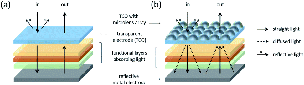 | ||
| Fig. 1 A scheme describing how incident light propagates in a material stack for organic photovoltaic devices in the (a) absence and (b) presence of a microlens array. | ||
Various microlens arrays with different materials and sizes
PDMS prepolymer and Norland Optical Adhesive (NOA) 63 prepolymer were introduced as the materials for the microlens arrays. Because the two materials have different chemical structures (Fig. 2a and b) and refractive indices. (The refractive index of PDMS is 1.43,45 while NOA 63 has a refractive index of 1.56.46), they were expected to induce different optical manipulation. The size of the microlens arrays was controlled from 0.5–10 μm by changing the sizes of the polystyrene microspheres while fabricating the master pattern. To confirm whether the arrays were well fabricated and desirably size-controlled, their morphologies were observed using AFM. Fig. 2c–h show AFM images of various microlens arrays of different sizes. All microlenses were well packed and ideally constructed without huge defects. The diameters of the microlenses were 0.5, 3, 5, 7, and 10 μm, respectively. Microlens arrays with different sizes had different curvatures for light incidence, which were expected to induce different optical manipulation in OPV devices. | ||
| Fig. 2 (a and b) The chemical structures of two different polymers used to prepare the microlens arrays; (a) poly(dimethylsiloxane) and (b) polyurethane-related polymer. (c–h) Atomic force microscope images of (c) a flat surface without a physical structure and microlens arrays having diameters of (d) 0.5 μm, (e) 3 μm, (f) 5 μm, (g) 7 μm, and (h) 10 μm, respectively. The scanning dimension of insets was 10 μm by 10 μm. | ||
Optical manipulation by microlens arrays with different materials
The optical manipulation capability of microlens arrays with different materials on ITO glass was measured with a half-sphere detector, as shown in Fig. 3a. First, to measure the amount of light reflected from the surface, a half-sphere detector was installed outside the microlens arrays. Because it covered 180° on the incoming side of the light, all reflective light from the microlens arrays was detected with a half-sphere detector, indicating total reflectance of the microlens arrays with different materials. Then, a half-sphere detector was installed inside the microlens arrays. Similarly, all light passing through the microlens arrays was detected, indicating the total transmittance of the microlens array. However, the total transmittance includes specular light going straight through the sample and diffused light refracting through the sample. To decouple two portions of the transmission light, a point detector was introduced and installed at the point where the light came in a straight line. This allowed us to measure the specular transmittance, and subtracting it from the total transmittance indicated the diffuse transmittance.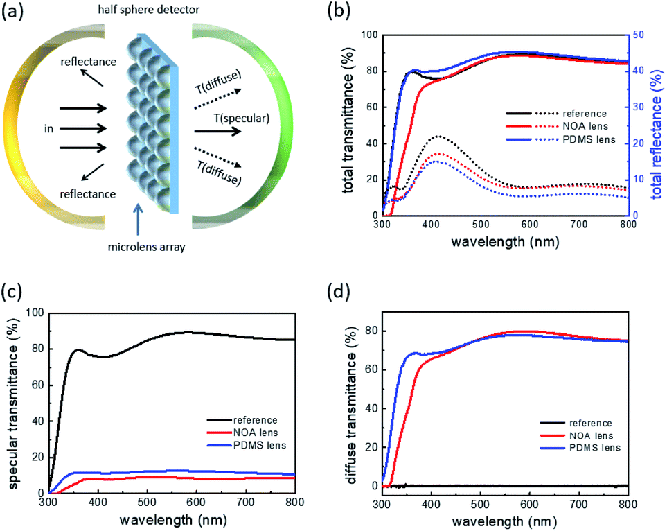 | ||
| Fig. 3 (a) A scheme to investigate the total reflectance and total transmittance of microlens array using a half-sphere detector. (b) Total transmittance (solid line), total reflectance (dashed line), (c) specular transmittance, and (d) diffuse transmittance of the reference without a microlens array and an ITO glass with a Norland Optical Adhesive microlens array and a poly(dimethylsiloxane) microlens array. | ||
Fig. 3b shows the total reflectance and total transmittance of the reference without a microlens array, an ITO glass with a NOA microlens array, and an ITO glass with a PDMS microlens array. The size of the microlens was fixed at 10 μm. The reference exhibited the highest reflectance of 21.9% and an average reflectance of 12.2% in the PTB7:PCBM absorption range (350–750 nm) for OPVs. When the microlens fabricated from NOA was introduced to ITO glass, the highest reflectance and average reflectance in the PTB7:PCBM absorption range were 17.2% and 10.3%, respectively, indicating an approximately 15.6% reduction in total reflectance compared to the reference. The PDMS microlens further reduced the total reflectance. It showed the highest reflectance of 15.1% and an average reflectance of 8.3% in the PTB7:PCBM absorption range. This indicates that most of the light can enter through ITO substrates with a PDMS microlens array. The total transmittance also changed with the materials of microlens. While the reference and NOA microlens showed an average total transmittance of approximately 83% in the PTB7:PCBM absorption range, the PDMS lens increased the total transmittance, leading to an average total transmittance of 86.4%.
However, although the total transmittance is high, the effective optical path may be short if all incident light goes straight. To separate the light that goes straight and the light that is distributed in various directions from the total transmittance, the specular transmittances were measured with a point detector, and diffuse transmittance was calculated by subtracting specular transmittance from the total transmittance. Fig. 3c and d show the specular and diffuse transmittance of the reference, an ITO glass with a NOA microlens array, and an ITO glass with a PDMS microlens array. In the reference, while specular transmittance was very high, diffuse transmittance was extremely low. Their averages were approximately 84% and below 1% in the absorption range, respectively. This indicates that most of the incident light goes straight through, so the effective optical path is short. When adopting the NOA microlens, the specular transmittance decreased, showing an average specular transmittance of 8.4% in the absorption range. On the other hand, the NOA microlens dramatically increased diffuse transmittance, representing an average diffuse transmittance of 73.7%. The ratio between specular and dispersive transmittance was approximately 9, indicating that most of the light is refracted through the microlens arrays, increasing the effective optical path. The PDMS microlens also decreased the specular transmittance and increased diffuse transmittance. They were approximately 11.9% and 74.6% in the PTB7:PCBM absorption range, respectively. In particular, it showed relatively high diffuse transmittance in the blue region compared to the NOA lens; the average diffuse transmittances from 350–450 nm were 62.3% and 69.0% in the NOA and PDMS microlens, respectively. Because blue has high energy, the high total and diffuse transmittance in the blue range indicates that more excitons were generated in the PDMS lens.
To probe that the better optical properties of microlens arrays induce higher light absorption, the extent of light extinction from the stacks of whole functional materials for OPVs was measured. Fig. 4 represents the total transmittance and total reflectance of whole stacks having microlens arrays that were prepared with different materials and the extinctions that were calculated from them. Because light excluding the reflected and transmitted light among incident light refers to the light that disappeared in the material stack, a simple calculation allows us to obtain the corresponding extinction value. The outer layer of OPV devices comprises a very reflective metal electrode. Therefore, the light cannot pass through the metal electrode, showing very low and comparable total transmittance through the material stack regardless of the material used for the microlens array. It was below 1% on average in the PTB7:PCBM absorption range. However, the reflectance was different depending on the materials used to fabricate the microlens array. While the NOA lens showed a 15.6% average reflectance in the absorption range, the average reflectance was 14.9% with the PDMS microlens array. This resulted in different extinction graphs depending on the materials used for the microlens array. As seen in Fig. 4b, the average extinction of the NOA lens in the absorption range was 84.3%, but PDMS had a higher extinction value of 85.0% while the reference showed an average extinction of 76.1%. Considering the UV absorption ability of NOA 63, which indicates that not all light is extinct in the photoactive layer, and the higher extinction value in the material stack with the PDMS microlens, the OPV with the PDMS microlens is expected to generate more electricity.
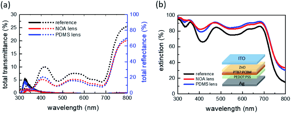 | ||
| Fig. 4 (a) Total transmittance (solid line), total reflectance (dashed line), and (b) extinction of material stacks for organic photovoltaics in the absence and presence of a microlens array. The inset represents the materials and architecture of material stacks. | ||
Optical manipulation by microlens arrays of different sizes
Microlens arrays with different sizes have different curvatures, inducing different light collecting and reflecting capabilities. To investigate the dependence of light manipulation capability on the microlens sizes, the total reflectance and transmittance of the microlens arrays (0.5–10 μm in size) on ITO glass without functional layer stacks were measured; because microlens over 10 μm showed comparable photovoltaic performance, optical analysis was performed up to 10 μm microlens (Fig. S1†). All microlenses were fabricated with PDMS. Fig. 5a shows the total reflectance and total transmittance of the microlens arrays having their sizes from 0.5 to 10 μm. Compared to the reflectance of the reference without a microlens array, the introduction of the microlens gradually decreased the total reflectance with increasing their sizes. Specifically, the reference showed 12.1% of average reflectance in the PTB7:PCBM absorption range, but microlens arrays with the size of 5 and 10 μm presented an average total reflectance of 8.9% and 8.2%, respectively, indicating a reduction in total reflectance of up to 32.2% with the PDMS microlens array compared to the reference. Decreasing total reflectance induced an increase in total transmittance with microlens arrays, leading to an average total transmittance of ∼87% with a 10 μm microlens array in the PTB7:PCBM absorption range from ∼84% in the reference. Then, the total transmittance was decoupled into specular and diffuse transmittance by measuring the specular transmittance and subtracting it from the total transmittance. Fig. 5b and c show specular and diffuse transmittance of ITO glass with microlens arrays of various sizes. As mentioned in the above section, the reference had very high specular transmittance and very low diffuse transmittance. The specular transmittance significantly decreased, and the diffuse transmittance dramatically increased with increasing microlens size. Specifically, the average specular transmittance and diffuse transmittance in the PTB7:PCBM absorption range were 80.1% and 3.8%, respectively, with a 0.5 μm microlens array. They became 45.9% and 39.6%, respectively, with a 3 μm microlens. After the sizes of the microlens reached 5 μm, the specular transmittance and diffuse transmittance were comparable. They were ∼12% and ∼75%, respectively. This indicates that the ratio between the specular and diffuse transmittance increased from below 0.1 in the reference to ∼6 with a 10 μm microlens. Haze also gradually increased with microlens size, representing about 80% in all spectral ranges with a 10 μm microlens (Fig. 5d). The dependence of refraction on the relative size of the physical structure to the wavelength of light resulted in different shapes of haze spectra depending on the microlens sizes. Because diffused light has a longer optical path compared to specular light, increasing the dispersive-to-specular transmittance ratio and haze are expected to induce high light absorption and exciton generation.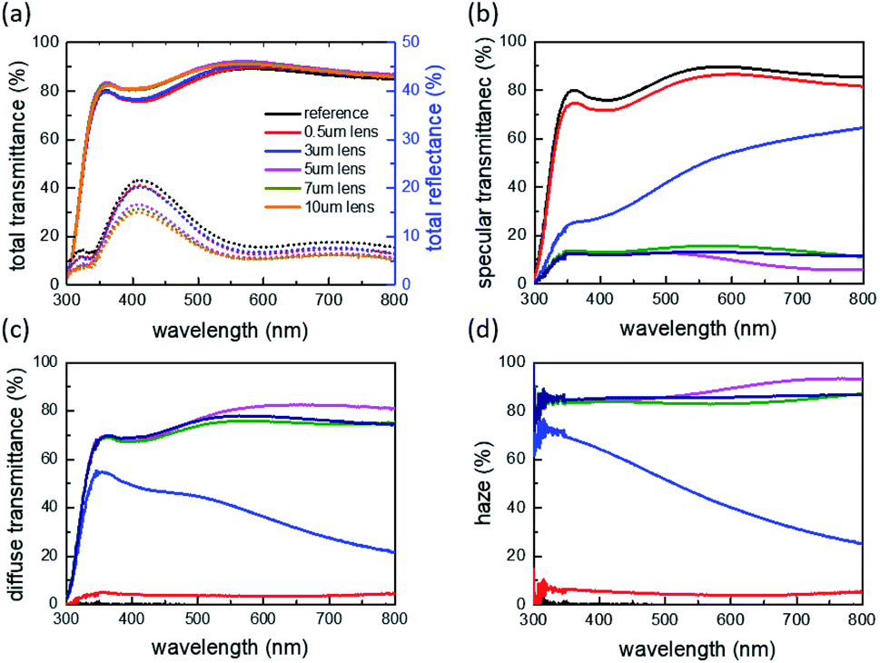 | ||
| Fig. 5 (a) Total transmittance (solid line), total reflectance (dashed line), (b) specular transmittance, (c) diffuse transmittance, and (d) haze of microlens arrays with different sizes from 0.5 to 10 μm. | ||
To ensure that a microlens with high total transmittance, high diffuse-to-specular transmittance ratio, and haze induced the better light absorption, total transmittance, and total reflection in the stacks of whole functional materials for OPVs were measured, followed by the calculation of extinction. Fig. 6a shows the total transmittance and total reflectance of whole material stacks having microlens arrays of different sizes. Similar to the above section, the material stack adopts a thin metal as the top electrode, so all material stacks with different microlens arrays showed very low average total transmittance values below 1% in the PTB7:PCBM absorption range. The total reflectance showed a similar shape because the microlenses were fabricated with the same materials but in different sizes. They showed the highest reflectance at blue wavelength and low reflectance at green and red wavelengths. However, the average reflectance in the PTB7:PCBM absorption range was strongly dependent on the size of the microlens. The highest reflectance at a peak near 425 nm was 34.4% in the reference. However, it began to decrease with increasing microlens size. It was 32.6% and 32.1% with 0.5 μm and 3 μm microlens, respectively. Then, it dramatically decreased with a 5 μm microlens, exhibiting 24.9% total reflectance, reaching 21.7% with a 10 μm microlens. The average reflectance in the PTB7:PCBM absorption range also decreased from 21.2% to 19.8%, 19.4%, 15.6%, 14.9%, and 13.5% for microlenses with sizes of 0.5 μm, 3 μm, 5 μm, 7 μm, and 10 μm, respectively. Different total reflectance depending on microlens sizes resulted in different extinctions. Fig. 6b shows the extinction values of various microlens arrays with different sizes. Similar to the reflectance graph, all showed similar features regardless of the microlens sizes. However, the average extinction in the PTB7:PCBM absorption range increased from 78.8% in the reference to 80.6% with a 3 μm microlens. It continued to increase with increasing microlens size, reaching 86.4% extinction with a 10 μm microlens array. It indicated that the microlens with a size of 10 μm can acquire approximately 10% more integrated photon energy in the PTB7:PCBM absorption range compared to the reference. The values were 752.2 eV in the reference and 823.2 eV with a 10 μm microlens, respectively, when integrating photon energy of extinction curves by multiplying the photon energy at each wavelength with the extinction value.
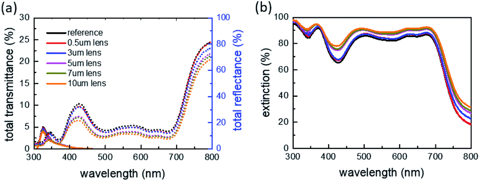 | ||
| Fig. 6 (a) Total transmittance (solid line), total reflectance (dashed line), and (b) extinction of materials stack for PTB7:PCBM devices with microlens arrays having different sizes from 0.5 to 10 μm. | ||
Correlation between optical characteristics and photovoltaic performance
To investigate whether high expectations really induce high performance in OPVs, the current density–voltage (J–V) characteristics of OPV devices with various microlens arrays were measured, and the real values of current generation were extracted from them. The real values were then correlated with the estimated current generation of material stacks for OPVs with various microlens arrays that were calculated with the extinctions and as-reported internal quantum efficiency.47–49 Fig. 7a shows the J–V characteristics of representative PTB7:PCBM OPVs with microlens arrays prepared with different materials. A PTB7:PCBM device without a microlens exhibited an open-circuit voltage of 0.76 ± 0.0 V and a short-circuit current density of 15.85 ± 0.83 mA cm−2, achieving a PCE of 7.54 ± 0.41%. When adopting microlens arrays, they exhibited comparable open-circuit voltage of approximately 0.77 V regardless of the materials used for the fabrication of the microlens because the open-circuit voltage is mainly determined by the energy level of the donor and acceptor materials,50,51 and identical material pairs were used to fabricate all photovoltaic devices. However, the short-circuit current density increased with the microlens array and was dependent on the materials of microlens array. Specifically, when a NOA microlens was used to fabricate the microlens array, the short-circuit current density increased by 5.7%, representing a short-circuit current density of 16.75 ± 0.58 mA cm−2. The PDMS microlens further enhanced the short-circuit current density. It showed a short-circuit current density of 17.60 ± 1.00 mA cm−2, which was 11.0% higher than that of the reference. This indicates that the estimation from optical properties of microlens arrays matched well with the real values from the J–V characteristics of various OPV devices with and without a microlens array. Therefore, we conclude that the PDMS microlens has higher total transmittance and more diffused light, inducing more light extinction and achieving greater electricity generation.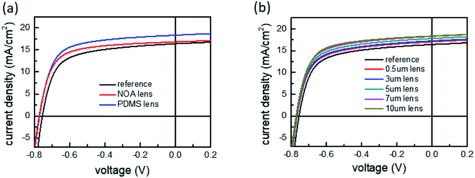 | ||
| Fig. 7 Current density–voltage characteristics of PTB7:PCBM organic photovoltaics with (a) microlens arrays that were prepared with different materials and (b) with microlens arrays with different sizes from 0.5 to 10 μm. | ||
Then, the actual current generation and the estimated current generation, depending on microlens sizes, were compared. Fig. 7b shows the J–V characteristics of representative PTB7:PCBM devices with PDMS microlens arrays of different sizes. Similar to the previous paragraph, all devices showed comparable open-circuit voltage at approximately 0.77 V because the same materials were used to fabricate the OPVs. The short-circuit current sequentially increased with increasing microlens size. They were 16.39 ± 0.89 mA cm−2, 16.45 ± 0.88 mA cm−2, 17.12 ± 0.92 mA cm−2, 17.47 ± 1.01 mA cm−2, and 17.60 ± 1.00 mA cm−2 in the reference and devices with microlens having diameters of 0.5 μm, 3 μm, 5 μm, 7 μm, and 10 μm, respectively. The device with 10 μm microlens array exhibited the best performance, showing a PCE of 9.45%, as summarized in Table 1. This trend was the same as the expectation from extinctions depending on microlens sizes.
| VOC (V) | JSC (mA cm−2) | FF | PCE (%) | |
|---|---|---|---|---|
| Reference | 0.76 ± 0.00 | 15.85 ± 0.83 | 0.63 ± 0.01 | 7.54 ± 0.41 (7.97*) |
| 0.5 μm lens | 0.77 ± 0.01 | 16.39 ± 0.89 | 0.63 ± 0.01 | 7.92 ± 0.45 (8.43*) |
| 3 μm lens | 0.77 ± 0.01 | 16.45 ± 0.88 | 0.63 ± 0.01 | 8.00 ± 0.48 (8.56*) |
| 5 μm lens | 0.77 ± 0.01 | 17.12 ± 0.92 | 0.64 ± 0.01 | 8.40 ± 0.49 (8.91*) |
| 7 μm lens | 0.77 ± 0.01 | 17.47 ± 1.01 | 0.64 ± 0.02 | 8.62 ± 0.65 (9.28*) |
| 10 μm lens | 0.77 ± 0.01 | 17.60 ± 1.00 | 0.65 ± 0.02 | 8.75 ± 0.71 (9.45*) |
To investigate the correlation between the estimated current generation and real current generation, the electron and current generation were calculated by multiplying the photon flux of the solar spectrum with the external quantum efficiency. External quantum efficiencies were acquired from the internal quantum efficiency and extinctions. The internal quantum efficiency was assumed to be 81%, which is similar to the value that has been previously reported.47–49 Fig. 8 shows the photon flux of the solar spectrum, the number of generated electrons, and the current generation depending on the wavelength. The reference device exhibited a total electron generation of 9.89 × 10²⁰ m−2, leading to a current generation of 15.85 mA cm−2. The device with a 3 μm microlens was expected to exhibit an electron generation of 1.02 × 10²¹ m−2, meaning a current of 16.32 mA cm−2. The 5 μm and 10 μm microlens were expected to generate more electrons and currents, reaching an electron generation of 1.07 × 10²¹ m−2 and 1.1 × 10²¹ m−2, and current generation of 17.17 mA cm−2 and 17.70 mA cm−2, respectively. The estimated values matched well with the real values from the J–V characteristics of various OPV devices with microlens arrays of different sizes. Therefore, measuring basic optical properties, such as the dispersive-to-specular transmittance ratio, helps to predict the final performance of OPV devices with physical structures.
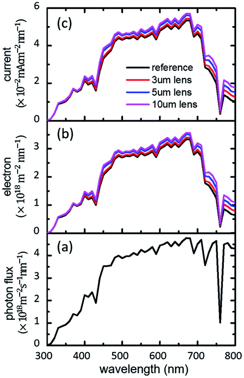 | ||
| Fig. 8 (a) Photon flux of solar spectrum (AM 1.5 G), and the estimated (b) electron and (c) current generation of materials stacks for PTB7:PCBM organic photovoltaics in the absence and presence of microlens arrays with sizes 3 μm, 5 μm, and 10 μm. | ||
Experimental
Construction of microlens arrays with different materials and sizes
To construct microlens arrays with different materials and sizes, master patterns with the engraved shape of the microlens were fabricated using the imprinting process. For the imprinting process, flat PDMS rubber with a thickness of 30 mm was prepared by mixing its prepolymer and curing agent (Sylgard 184 A& B, Dow Corning) at a weight ratio of 10![[thin space (1/6-em)]](https://www.rsc.org/images/entities/char_2009.gif) :1 and curing it in the flat Petri dishes at 80 °C for 4 h. Polystyrene microspheres (Alfa Aesar) with various sizes from 0.5 to 10 μm were aligned on a flat PDMS rubber using water transfer or rubbing methods, as reported elsewhere.52–54 Then, a silicon wafer was ultrasonically cleaned with acetone (Daejung) and isopropyl alcohol (IPA, Daejung) at 60 °C for 10 min. After drying at 100 °C for 30 min, SU-8 2015(Microchem) was coated on it at 800 rpm for 10 s and then 3000 rpm for 120 s. Finally, SU-8 on the silicon wafer was imprinted using a PDMS stamp with polystyrene spheres, followed by curing under 365 nm ultraviolet light illumination for 1 h and delaminating the PDMS stamp from SU-8. Because the array of polystyrene spheres had an embossed microlens structure and polystyrenes were not chemically reacted with the SU-8 substrate, pressing SU-8 with polystyrene spheres changed the shape of the non-hardened SU-8 into the engraved microlens structure and polystyrenes were stuck in SU-8 during the imprinting process. Then, polystyrene spheres on SU-8 were dissolved in toluene (Samchun), completing the fabrication of SU-8 master patterns with engraved structures of various sizes depending on the size of the microspheres. To construct microlens arrays for OPVs from the master patterns, the prepolymer, PDMS prepolymer or urethane-related prepolymer (NOA 63), was poured into the master mold, followed by curing. The PDMS prepolymer was cured at 80 °C for 4 h, while NOA 63 was cured under 365 nm ultraviolet light for 1 h. The delamination of the polymer from the master patterns was completed to construct microlens arrays with different materials and sizes. The morphology of the microlens arrays was observed using an atomic force microscope (AFM, XE-100, Park Systems) to confirm that they were well constructed.
:1 and curing it in the flat Petri dishes at 80 °C for 4 h. Polystyrene microspheres (Alfa Aesar) with various sizes from 0.5 to 10 μm were aligned on a flat PDMS rubber using water transfer or rubbing methods, as reported elsewhere.52–54 Then, a silicon wafer was ultrasonically cleaned with acetone (Daejung) and isopropyl alcohol (IPA, Daejung) at 60 °C for 10 min. After drying at 100 °C for 30 min, SU-8 2015(Microchem) was coated on it at 800 rpm for 10 s and then 3000 rpm for 120 s. Finally, SU-8 on the silicon wafer was imprinted using a PDMS stamp with polystyrene spheres, followed by curing under 365 nm ultraviolet light illumination for 1 h and delaminating the PDMS stamp from SU-8. Because the array of polystyrene spheres had an embossed microlens structure and polystyrenes were not chemically reacted with the SU-8 substrate, pressing SU-8 with polystyrene spheres changed the shape of the non-hardened SU-8 into the engraved microlens structure and polystyrenes were stuck in SU-8 during the imprinting process. Then, polystyrene spheres on SU-8 were dissolved in toluene (Samchun), completing the fabrication of SU-8 master patterns with engraved structures of various sizes depending on the size of the microspheres. To construct microlens arrays for OPVs from the master patterns, the prepolymer, PDMS prepolymer or urethane-related prepolymer (NOA 63), was poured into the master mold, followed by curing. The PDMS prepolymer was cured at 80 °C for 4 h, while NOA 63 was cured under 365 nm ultraviolet light for 1 h. The delamination of the polymer from the master patterns was completed to construct microlens arrays with different materials and sizes. The morphology of the microlens arrays was observed using an atomic force microscope (AFM, XE-100, Park Systems) to confirm that they were well constructed.
Fabrication of organic photovoltaic devices
The transparent conducting electrode, ITO, was cleaned with acetone and IPA at 60 °C for 15 min to construct organic photovoltaic cells. After preparing the zinc oxide precursor solution with zinc acetate dehydrate (Sigma Aldrich), as reported elsewhere,55,56 it was spin-coated on pre-cleaned ITO glass at 2000 rpm for 100 s. Annealing at 200 °C for 10 min completed the formation of an 85 nm thick zinc oxide electron transport layer. Then, a cosolution of poly[4,8-bis[(2-ethylhexyl)oxy]benzo[1,2-b:4,5-b]dithiophene-2,6-diyl][3-fluoro-2-[(2-ethylhexyl)carbonyl]thieno[3,4-b]thiophenediyl] ((C41H53FO4S4)n, PTB7) and [6,6]-phenyl-C71-butyric acid (C82H14O2, PC71BM) was spin-coated on the zinc oxide layer at 1000 rpm for 60 s as a photoactive layer to absorb incident light. The photoactive layer solution was prepared by mixing PTB7 (8 mg, 1-materials) and PCBM (12 mg, Nano-c) in chlorobenzene (970 μL, Sigma Aldrich), followed by the addition of 1,8-diiodooctane (30 μL, Sigma Aldrich). The hole transport layer was formed on the photoactive layer by spin-coating a diluted poly(3,4-ethylenedioxythiophene):poly (styrene sulfonate) (PEDOT:PSS, Clevios PVP Al 4083, Heraeus) solution in IPA (1:10 v/v) at 5000 rpm for 60 s, and then dried at 120 °C for 1 min. Thermal evaporation of a 100 nm thick silver electrode through a stencil mask was completed to construct PTB7:PCBM organic photovoltaics with an inverted architecture.
Characterization of light manipulation capability and photovoltaic performance
The optical manipulation using the microlens itself and the functional layer stacks with microlens arrays for OPVs were measured through ultraviolet-visible (UV/Vis, Cary 6000, Agilent) spectroscopy with point and half-sphere detectors. To evaluate the optical manipulation capability of the microlens itself, total transmittance, specular transmittance, and total reflectance were measured after loading the microlens array film into the sample holder of UV-Vis spectroscopy. The diffuse transmittance was then calculated from the total transmittance and specular transmittance. To optically evaluate the microlens in the functional layer stacks, the microlens array was attached to the ITO glass of pre-fabricated PTB7:PCBM OPVs. After measuring the total transmittance and total reflectance with a half-sphere detector, the extinction, the light disappearing in the functional layer, was calculated by subtracting them from the input light. Photovoltaic performances were characterized by measuring the J–V characteristics under AM 1.5 G 100 mW cm−2 illumination. A solar simulator (ORIEL LCS-100, Newport) and a Keithley 2400 were used as the light source and power source meter, respectively.Conclusions
We analyzed how incident light propagates in microlens array films and functional material stacks for OPVs depending on the materials and sizes of the microlens array. PDMS exhibited less reflection of incident light and higher diffuse transmittance than NOA 63, resulting in higher extinction and current generation in the OPV architecture. The microlens sizes also controlled the total and diffuse transmittance, affecting light extinction and current generation. The total and diffuse transmittance generally increased with increasing microlens size, exhibiting an average extinction of 86.4% and the highest PCE of 9.45% with a 10 μm microlens. The estimated current density from extinction correlated well with the real current generation of OPV devices with microlens arrays. This indicates that the optical characterization of physical structures, including the control of light propagation, allows to expect the improvement of current generation in OPVs.Conflicts of interest
There are no conflicts to declare.Acknowledgements
This work was supported by the Energy Technology Development Project of the Korea Institute of Energy Technology Evaluation and Planning (KETEP) granted financial resource from the Ministry of Trade, Industry & Energy, Republic of Korea (No. 1711026557), and the National Research Foundation of Korea Grant funded by the Korean Government (NRF-2018R1A6A1A03025761). J. Kim also acknowledges the Basic Science Research Program through the National Research Foundation of Korea (NRF) funded by the Ministry of Education (NRF-2018R1D1A1B07049736).References
- K. Gao, Y. Kan, X. Chen, F. Liu, B. Kan, L. Nian, X. Wan, Y. Chen, X. Peng, T. P. Russell, Y. Cao and A. K.-Y. Jen, Adv. Mater., 2020, 32, 1906129 CrossRef PubMed.
- S. M. McAfee, S. V. Dayneko, A. D. Hendsbee, P. Josse, P. Blanchard, C. Cabanetos and G. C. Welch, J. Mater. Chem. A, 2017, 5, 11623 RSC.
- G. Zhang, J. Zhao, P. C. Y. Chow, K. Jiang, J. Zhang, Z. Zhu, J. Zhang, F. Huang and H. Yan, Chem. Rev., 2018, 118, 3447 CrossRef CAS PubMed.
- T.-W. Chen, C.-C. Chang, Y.-T. Hsiao, C. Chan, L. Hong, L. Zhong, W.-T. Chuang, J. Hou, Y. Li and C.-S. Hsu, ACS Appl. Mater. Interfaces, 2019, 11, 31069 CrossRef CAS.
- G. Li, W. Yang, S. Wang, T. Liu, C. Yan, G. Li, Y. Zhang, D. Li, X. Wang, P. Hao, J. Li, L. Huo, H. Yan and B. Tang, J. Mater. Chem. C, 2019, 7, 10901 RSC.
- T. Wang, R. Sun, S. Xu, J. Guo, W. Wang, J. Guo, X. Jiao, J. Wang, S. Jia, X. Zhu, Y. Li and J. Min, J. Mater. Chem. A, 2019, 7, 14070 RSC.
- W. Zhao, S. Li, H. Yao, S. Zhang, Y. Zhang, B. Yang and J. Hou, J. Am. Chem. Soc., 2017, 139, 7148 CrossRef CAS.
- S. Zhang, Y. Qin, J. Zhu and J. Hou, Adv. Mater., 2018, 30, 180868 Search PubMed.
- H.-H. Gao, Y. Sun, X. Wan, X. Ke, H. Feng, B. Kan, Y. Wang, Y. Zhang, C. Li and Y. Chen, Adv. Sci., 2018, 5, 1800307 CrossRef.
- Y. Xie, F. Yang, Y. Li, M. A. Uddin, P. Bi, B. Fan, Y. Cai, X. Hao, H. Y. Woo, W. Li, F. Liu and Y. Sun, Adv. Mater., 2018, 30, 1803045 CrossRef.
- J. Song, C. Li, L. Zhu, J. Guo, J. Xu, X. Zhang, K. Weng, K. Zhang, J. Min, X. Hao, Y. Zhang, F. Liu and Y. Sun, Adv. Mater., 2019, 31, 1905645 CrossRef CAS PubMed.
- L. Zhan, S. Li, T.-K. Lau, Y. Cui, X. Lu, M. Shi, C.-Z. Li, H. Li, J. Hou and H. Chen, Energy Environ. Sci., 2020, 13, 635 RSC.
- J. Gao, W. Gao, X. Ma, Z. Hu, C. Xu, X. Wang, Q. An, C. Yang, X. Zhang and F. Zhang, Energy Environ. Sci., 2020, 13, 958 RSC.
- Y. Lin, B. Adilbekova, Y. Firdaus, E. Yengel, H. Faber, M. Sjjad, X. Zheng, E. Yarali, A. Seitkhan, O. M. Bakr, A. El-Labban, U. Schwingenschlögl, V. Tung, I. McCulloch, F. Laquai and T. D. Anthopoulos, Adv. Mater., 2019, 31, 1902965 CrossRef CAS.
- B. O`Connor, C. Haughn, K.-H. An, K. P. Pipe and M. Shtein, Appl. Phys. Lett., 2008, 93, 223304 CrossRef.
- J. Zhong, Z. Xiao, W. Liang, Y. Wu, Q. Ye, H. Xu, H. Deng, L. Shen, X. Feng and Y. Long, ACS Appl. Mater. Interfaces, 2019, 11, 47992 CrossRef CAS.
- S. Schubert, J. Meiss, L. Müller-Meskamp and K. Leo, Adv. Energy Mater., 2013, 3, 438 CrossRef CAS.
- K.-S. Chen, H.-L. Yip, J.-F. Salinas, Y.-X. Xu, C.-C. Chueh and A. K.-Y. Jen, Adv. Mater., 2014, 26, 3349 CrossRef CAS PubMed.
- S. Chen, H. Dong, L. He, S. Xiang and J. Huang, Org. Electron., 2020, 79, 105636 CrossRef CAS.
- Y. Wang, P. Shem, J. Liu, Y. Xue, Y. Wang, M. Yao and L. Shen, Sol. RRL, 2019, 3, 1900181 CrossRef.
- H. Li, Y. Lv, X. Zhang, X. Wang and X. Liu, Sol. Energy Mater. Sol. Cells, 2015, 136, 86 CrossRef CAS.
- W. J. Dong, J. Y. Park, J. Ham, G. H. Jung, I. Lee and J.-L. Lee, Adv. Funct. Mater., 2016, 26, 5437 CrossRef CAS.
- Q.-D. Ou, Y.-Q. Li and J.-X. Tang, Adv. Sci., 2016, 3, 1600123 CrossRef PubMed.
- C.-C. Chueh, M. Crump and A. K.-Y. Jen, Adv. Funct. Mater., 2016, 26, 321 CrossRef CAS.
- X. Yu, Y. Yuan, J. Xu, K.-T. Yong, J. Qu and J. Song, Laser Photonics Rev., 2019, 13, 1800219 CrossRef.
- K. Li, Y. Zhang, H. Zhen, H. Wang, S. Liu, F. Yan and Z. Zheng, J. Mater. Chem. A, 2017, 5, 969 RSC.
- K. Li, R. Wu, Y. Ruan, L. Zhang and H. Zhen, Sol. Energy, 2018, 170, 800 CrossRef.
- D. H. Kim, B. Dudem, J. W. Jung and J. S. Yu, ACS Appl. Mater. Interfaces, 2018, 10, 13113 CrossRef CAS.
- C. Fang, Z. Yang, J. Zhang, Y. Zhuang, S. Liu, X. He and Y. Zhang, Sol. Energy Mater. Sol. Cells, 2020, 206, 110305 CrossRef CAS.
- Y. Chen, M. Elshobaki, Z. Ye, J.-M. Park, M. A. Noack, K.-M. Ho and S. Chaudhary, Phys. Chem. Chem. Phys., 2013, 15, 4297 RSC.
- J.-D. Chen, L. Zhou, Q.-D. Ou, Y.-Q. Li, S. Shen, S.-T. Lee and J.-X. Tang, Adv. Energy Mater., 2014, 4, 1301777 CrossRef.
- M. Tai, X. Zhao, H. Shen, Y. Guo, M. Zhang, Y. Zhou, X. Li, Z. Yao, X. Yin, J. Han, X. Li and H. Lin, Chem. Eng. J., 2019, 361, 60 CrossRef CAS.
- M. M. Tavakoli, A. Simchi, R. Tavakoli and Z. Fan, J. Phys. Chem. C, 2017, 121, 9757 CrossRef CAS.
- R. M. Howden, E. J. Flores, V. Bulović and K. K. Cleason, Org. Electron., 2013, 14, 2257 CrossRef CAS.
- S.-F. Leung, Q. Zhang, F. Xiu, D. Yu, J. C. Ho, D. Li and Z. Fan, J. Phys. Chem. Lett., 2014, 5, 1479 CrossRef CAS PubMed.
- L. Meng, H. Chai, X. Yang, Z. Lv and T. Yang, Sol. Energy Mater. Sol. Cells, 2019, 191, 459 CrossRef CAS.
- X. Wang, Z. Liu, Z. Yang, J. He, X. Yang, T. Yu, P. Gao and J. Ye, Small, 2018, 14, 1704493 CrossRef.
- P. Singh, S. K. Srivastava, B. Sivaiah, P. Prathap and C. M. S. Rauthan, Sol. Energy, 2018, 170, 221 CrossRef CAS.
- S. Esiner, T. Bus, M. M. Wienk, K. Hermans and R. A. J. Janssen, Adv. Energy Mater., 2013, 3, 1013 CrossRef CAS.
- C. Cho, H. Kim, S. Jeong, S.-W. Paek, J.-W. Seo, D. Han, K. Kim, Y. Park, S. Yoo and J.-Y. Lee, Sol. Energy Mater. Sol. Cells, 2013, 115, 36 CrossRef CAS.
- Y. Li, Y. Zhang, J. Lin, C. Fang, Y. Ke, H. Tao, W. Wang, X. Zhao, Z. Li and Z. Lin, Appl. Surf. Sci., 2018, 462, 105 CrossRef CAS.
- S. Y. Ryu, J. H. Seo, H. Hafeez, M. Song, J. Y. Shin, D. H. Kim, Y. C. Jung and C. S. Kim, J. Phys. Chem. C, 2017, 121, 9191 CrossRef CAS.
- J. B. Kim, P. Kim, N. C. Pégard, S. J. Oh, C. R. Kagan, J. W. Fleischer, H. A. Stone and Y.-L. Loo, Nat. Photonics, 2012, 6, 327 CrossRef CAS.
- B. Olyaeefar, A. Asgari and S. Ahmadi-kandjani, Sol. Energy Mater. Sol. Cells, 2020, 215, 110688 CrossRef CAS.
- V. Prajzler, M. Neruda and P. Nekvindova, J. Mater. Sci.: Mater. Electron., 2018, 29, 5878 CrossRef CAS.
- J. D. Myers, W. Cao, S.-H. Eom, R. Zhou, L. Yang, W. You and J. Xue, Energy Environ. Sci., 2012, 5, 6900 RSC.
- Q. Amargos-Reyes, J. Maldonado, D. Romero-Borja, D. Barreiro-Arguelles, I. Caballero-Quintana, O. Barbosa-Garcia and J. A. Gaspar, J. Mater. Sci., 2019, 54, 2427 CrossRef.
- S. M. Menke, A. Cheminal, P. Conaghan, N. A. Ran, N. C. Greehnam, G. C. Bazan, T.-Q. Nguyen, A. Rao and R. H. Friend, Nat. Commun., 2018, 9, 277 CrossRef.
- L. J. A. Koster, S. E. Shaheen and J. C. Hummelen, Adv. Energy Mater., 2012, 2, 1246 CrossRef CAS.
- S. Gunes, H. Neugebauer and N. S. Sariciftci, Chem. Rev., 2007, 107, 1324 CrossRef PubMed.
- J. B. Kim, Z.-L. Guan, A. L. Shu, A. Kahn and Y.-L. Loo, Langmuir, 2011, 27, 11265 CrossRef CAS PubMed.
- J. C. Yang and J. Y. Park, ACS Appl. Mater. Interfaces, 2016, 8, 7381 CrossRef CAS.
- K. Koh, H. Hwang, C. Park, J. Y. Lee, T. Y. Jeon, S.-H. Kim, J. K. Kim and U. Jeong, ACS Appl. Mater. Interfaces, 2016, 8, 28149 CrossRef CAS.
- C. Park, T. Lee, Y. Xia, T. J. Shin, J. Myoung and U. Jeong, Adv. Mater., 2014, 26, 4633 CrossRef CAS.
- D. Ko, B. Gu, S. J. Kang, S. Jo, D. C. Hyun, C. S. Kim and J. Kim, J. Mater. Chem. A, 2019, 7, 14536 RSC.
- H. Song, Y. Ma, D. Ko, S. Jo, D. C. Hyun, C. S. Kim, H.-J. Oh and J. Kim, Appl. Surf. Sci., 2020, 512, 145660 CrossRef CAS.
Footnote |
| † Electronic supplementary information (ESI) available. See DOI: 10.1039/d0ra09262b |
| This journal is © The Royal Society of Chemistry 2021 |