
A naphthalene diimide side-chain polymer as an electron-extraction layer for stable perovskite solar cells†
Khaled
Al Kurdi
 a,
Declan P.
McCarthy
a,
David P.
McMeekin
bc,
Sebastian O.
Furer
bc,
Marie-Hélène
Tremblay
a,
Stephen
Barlow
a,
Udo
Bach
bc and
Seth R.
Marder
*a
a,
Declan P.
McCarthy
a,
David P.
McMeekin
bc,
Sebastian O.
Furer
bc,
Marie-Hélène
Tremblay
a,
Stephen
Barlow
a,
Udo
Bach
bc and
Seth R.
Marder
*a
aSchool of Chemistry and Biochemistry, Georgia Institute of Technology, Atlanta, GA 30332, USA. E-mail: seth.marder@chemistry.gatech.edu
bAustralian Research Council Centre of Excellence in Exciton Science, Department of Chemical Engineering, Monash University, Clayton, Victoria 3800, Australia
cDepartment of Chemical Engineering, Monash University, Clayton, Victoria 3800, Australia
First published on 5th November 2020
Abstract
Poly(N-(5-(5-norbornene-2-carbonyl)oxy)pentyl)-N′-n-hexyl-naphthalene-1,8:4,5-bis(dicarboximide) has been synthesized by esterification of (N-(5-hydroxypentyl)-N′-n-hexyl-naphthalene-1,8:4,5-bis(dicarboximide)) with exo-5-norbornene-2-carboxylic acid, and has been polymerized using the first-generation Grubbs initiator. This side-chain polymer exhibits good transparency throughout the visible (absorption onset at ca. 400 nm), good solubility in common low- and medium-polarity organic solvents, good resistance to dimethylformamide, and appropriate electron affinity for use as an electron-extraction layer in lead-halide perovskite solar cells. The performance of this polymer in n-i-p perovskite solar cells was compared to that of several small-molecule naphthalene-1,8:4,5-bis(dicarboximide) derivatives and of SnO2. Solar cells using the polymer exhibited open-circuit voltages of up to 1.02 V, short-circuit currents of over 21 mA cm−2, and power conversion efficiencies (PCE) reaching 14% which stabilize at 13.8% upon 90 s of illumination. Meanwhile control SnO2 devices exhibited a PCE of ca. 16%, and small-molecule devices gave PCE values of less than 10%. The devices employing the polymer exhibited improved long-term stability relative to the SnO2 control devices under continuous illumination.
Introduction
Lead-halide perovskite solar cells (PSCs) have received increasing attention since their debut in 2009.1,2 In recent years, further optimizations of the various layers and interfaces have allowed the emergence of PSCs with efficiencies exceeding 25%.3 Hole- and electron-transport materials (HTMs and ETMs, respectively) in PSCs serve not only to transport charges, but also to improve the stability of the cells and to reduce charge recombination. A variety of organic and inorganic ETMs have been incorporated into n-i-p (negative-intrinsic-positive) and p-i-n (positive-intrinsic-negative) PSCs.4–7The “regular” (n-i-p) architecture for PSCs requires the ETM to be deposited prior to the perovskite, and, therefore, for solution-processed cells, to be insoluble in the perovskite precursor solution. Insoluble metal oxides (e.g., SnO2, TiO2) offer one possible solution.8–10 Although many approaches require high-temperature (often 450–500 °C for TiO28,9) sintering subsequent to casting the precursors from solution, limiting compatibility with flexible substrates, recently room-temperature methods for the deposition of efficient SnO2 layers have been reported.11 Nevertheless, these oxides can possess trap states that hinder charge extraction and TiO2 can even act as a photocatalyst. There is also considerable interest in organic ETMs as alternatives that can be processed at low temperature, while also exhibiting good charge-transport abilities and transparency.12–15 These include both vacuum-processable and solution-processed materials;16 in some cases solution-processable ETMs have been crosslinked subsequent to deposition to prevent their dissolution during subsequent perovskite deposition.17,18 Although fullerenes have been widely used, non-fullerene electron acceptors with similar reduction potentials may be advantageous in terms of transparency, cost, and/or tunability of reduction potential. Rylene diimides have attracted attention as ETMs for n-i-p cells. These include perylene diimides, such as B (Fig. 1), and related thermally evaporable small molecules,19 solution-processable small molecules,20 and solution-processable polymers.21 Naphthalene diimide (NDI) derivatives (such as D and E, Fig. 1) have been used in p-i-n devices,22–25 but there are few reports of their use in n-i-p devices. However, in one study an insoluble NDI (A, Fig. 1) was generated via high-annealing treatment of soluble solution-cast precursor for use in n-i-p devices.26 A coronene diimide small molecule (C, Fig. 1) has also been used.27 Unlike their perylene and coronene counterparts, naphthalene diimides (NDI) can exhibit minimal absorption within the visible spectrum.
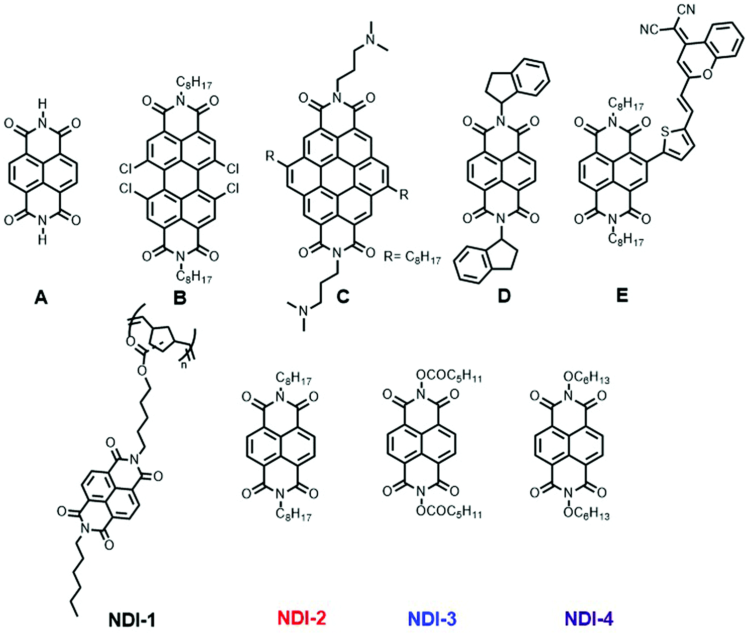 | ||
| Fig. 1 Examples of rylene diimide ETMs reported in the literature (A–E) in the context of PSCs and NDI-based ETMs used in this work (1–4). | ||
Since polymeric HTMs such as PEDOT:PSS, P3HT, PTAA, and polyTPD28–31 have been reported to give impressive performances in PSCs (PCE > 19%), it may be beneficial to examine electron-transporting polymers that are transparent in the visible, with appropriate electron affinities, electron mobility, solvent resistance, and solution processability. Moreover, such polymers may facilitate a “polymer sandwich” architecture in which both transport materials are polymeric, and which may be particularly useful for flexible devices.
In this work, we report a new NDI side-chain polymer (Fig. 1), which is transparent, solution processable, and thermally stable, and which can be used to fabricate n-i-p devices with efficiencies up to 14%. The utility of the polymer is illustrated by comparison to other NDI small molecules as well as SnO2 as a reference.
Results and discussion
Synthesis
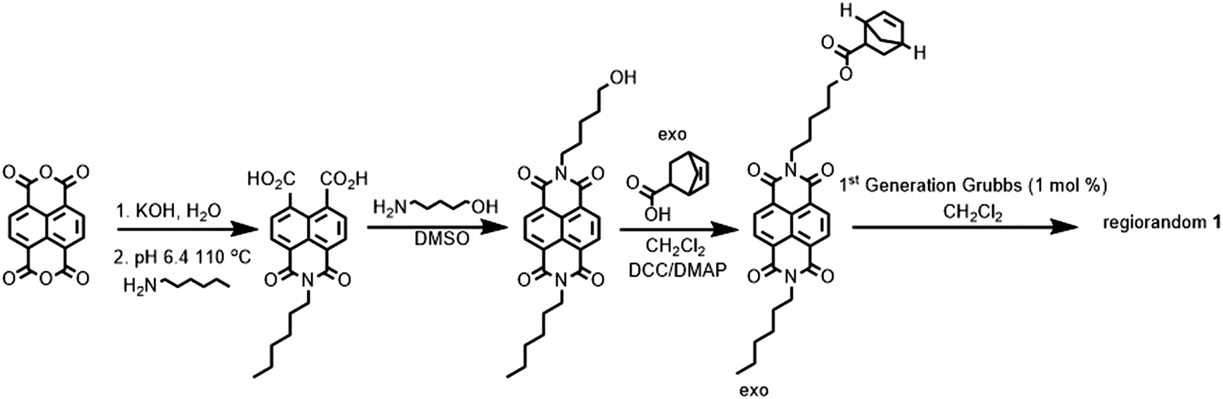
A naphthalene diimide polymer may help reduce aggregation and crystallization and, thus aid the formation of uniform continuous (i.e. pinhole free) thin films with reduced shunt paths between the transparent conducting oxide (TCO) and the perovskite. Although conjugated NDI polymers are well established and have been used in p-i-n cells, many absorb strongly throughout the visible spectrum, competing with perovskite layer light absorption.32 Accordingly, we chose to synthesize a side-chain polymer, which was expected to be colorless (NDI-1, Fig. 1). The polymer synthesis (Scheme 1) involves four steps, the first of which is an asymmetric imidization of the commercially available naphthalene tetracarboxy-1,8:4,5-dianhydride. The second step involves the imidization of N-hexyl-naphthalene-1,8-dicarboximide-4,5-di(carboxylic acid) with 5-amino-1-pentanol to afford the asymmetric hydroxyl-functionalized naphthalene diimide. Thirdly, the monomer is produced by esterification using exo-5-norbornenecarboxylic acid. Lastly, the regiorandom polymer NDI-1 (Mn = 13.3 kDa, Đ = 1.3) is produced via ring-opening metathesis polymerization using the Grubbs first-generation initiator, Ru(![[double bond, length as m-dash]](https://www.rsc.org/images/entities/char_e001.gif) CHPh)(PCy3)2Cl2 (Cy = cyclohexyl) (Fig. S1 and S2, ESI†). Several small-molecule NDI molecules (2–4) were synthesized for comparison according to published procedures,33 and were chosen to exhibit a range of reduction potentials.
CHPh)(PCy3)2Cl2 (Cy = cyclohexyl) (Fig. S1 and S2, ESI†). Several small-molecule NDI molecules (2–4) were synthesized for comparison according to published procedures,33 and were chosen to exhibit a range of reduction potentials.
 | ||
| Scheme 1 Synthesis of side chain NDI polymer (NDI-1) | ||
Characterization of the ETMs
Fig. 2A shows absorption spectra for NDI-1 in solution and in films, while Table 1 gives absorption maxima for NDIs 1–4. Both solution and films of the NDI derivatives exhibit absorptions onsets at wavelengths shorter than 400 nm. Although scattering is evident for films in the visible range, the transmittance for a 30 nm-thick film still exceeds 80% through the visible region (400–800 nm) (Fig. S7, ESI†). The electron affinities of ETMs are critical for efficient charge extraction from the perovskite; the reduction potentials were estimated from cyclic voltammetry (Fig. S3, ESI†, Table 1) and fall into a similar range to other molecular materials successfully used as ETMs in PSCs (such as C60 (−0.98 V), PCBM (−1.1 V), and N2200 (−1.1 V)).32,34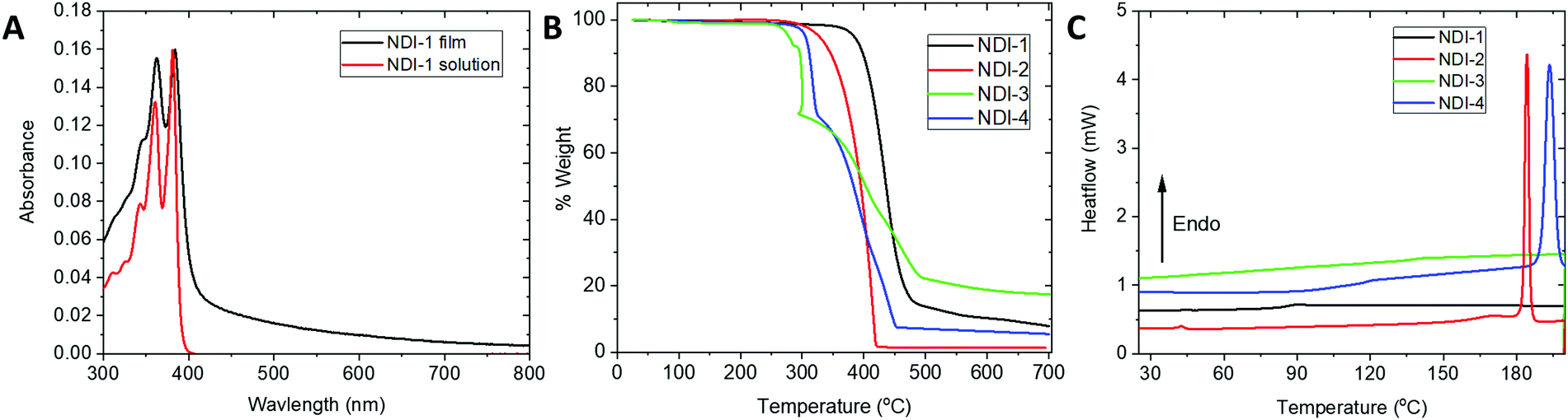 | ||
| Fig. 2 Absorption spectra of NDI-1 in solution and thin film (A), TGA (B) and DSC (C) plots of NDI molecules used in this work. TGA and DSC were performed under nitrogen gas at 10 °C min−1 scan rate. | ||
| Compound | λ max (nm) | E g (eV) | T m (°C) | T d (°C) | E 1/2 red (V) |
|---|---|---|---|---|---|
| a UV-vis is measured in chlorobenzene. b Optical bandgap is determined from absorption edge. c DSC/TGA is done under nitrogen gas at 10 °C min−1 scan rate, and Td is determined at 95% mass. d E 1/2 red vs. FeCp2+/0 (CH2Cl2/0.1 M NBu4PF6); data for NDI-1 were acquired using the corresponding monomer. | |||||
| NDI-1 | 381 | 3.1 | — | 384 | −1.11 |
| NDI-2 | 376 | 3.1 | 180 | 328 | −1.1433 |
| NDI-3 | 376 | 3.2 | — | 274 | −0.8833 |
| NDI-4 | 379 | 3.2 | 195 | 305 | −0.9633 |
The four NDI materials are highly soluble in common organic solvents (chloroform, dichloromethane, toluene), suggesting that they could be readily processed onto perovskite films for p-i-n devices without significant damage to the active layer. They exhibit varying resistance to N,N-dimethylformamide and dimethyl sulfoxide (DMF and DMSO respectively, Fig. S9 and S10, ESI†). The DMF resistance of NDI-1 is particularly promising for the fabrication of n-i-p device architectures; the small molecules are more easily removed by this solvent, although they are expected to less soluble in concentrated solutions of perovskite precursors and when protected by the alumina interlayer. Thermogravimetric analysis (TGA) and differential scanning calorimetry (DSC) show that the naphthalene diimides examined here exhibit decomposition temperatures above 250 °C and no thermal transitions below 150 °C, which is compatible with temperatures needed for subsequent deposition and annealing of many hybrid perovskites used in PSCs (Fig. 2B and C).
Device architecture and performance
The materials were incorporated into n-i-p devices (Fig. 3). The NDI layers were spin-coated from chlorobenzene on fluorinated-tin-oxide (FTO) coated glass (optimally performing layers having thicknesses of ca. 10 nm). A thin mesoporous layer of alumina nanoparticles was found to be very helpful in achieving subsequent good coating of the ETM by the perovskite. Although primarily used in the present case to enhance the wettability of the perovskite solution on the NDI films, the alumina nanoparticles may play other roles, as discussed in the literature.35–37 For example, at least when used between oxide transport materials and perovskites, a mesoporous alumina layer leads to improved contact between the transport and active layers,36 and in some cases the use of alumina leads to improved stability for the perovskite.37 They may also help protect the ETM from dissolution in the perovskite casting solvent (primarily DMF). Fig. 3A schematically shows the structure of the resulting solar cell incorporating the insulating alumina scaffold.38 Our control devices employed a SnO2 ETL layer instead of the NDI-based material. A mixed-cation perovskite Cs0.05FA0.79MA0.16PbI2.49Br0.51 (FA = formamidinium; MA = methylammonium) was then deposited via the solvent-quenching approach using chlorobenzene as an anti-solvent.39–42 Spiro-OMeTAD, with lithium bis(trifluoromethanesulfonyl)imide (LiTFSI) and 4-tert-butylpyridine (tBP) as additives, was then deposited on top as the hole transport layer, followed by evaporating 80 nm layer of gold as a counter electrode.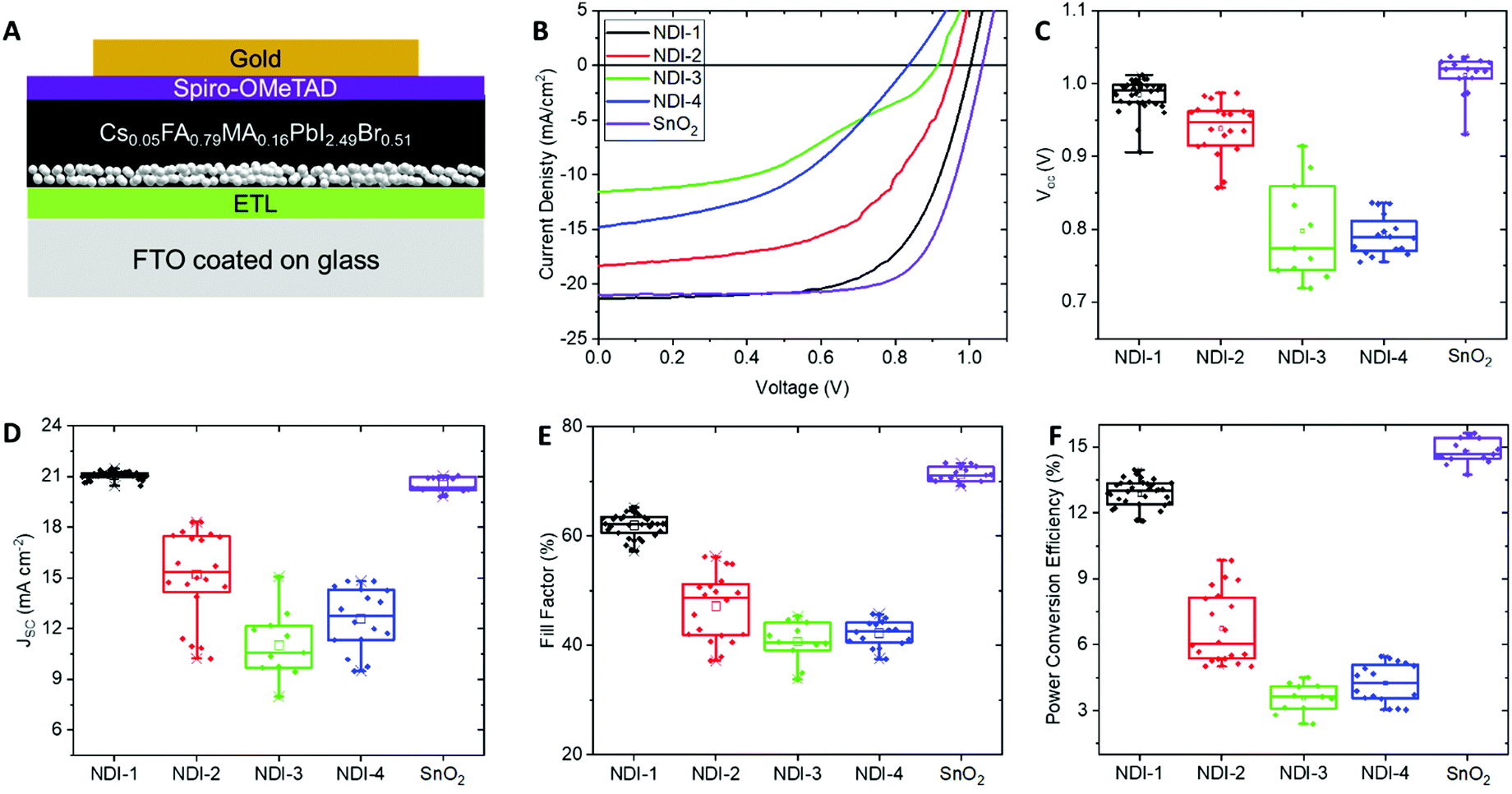 | ||
| Fig. 3 Schematic representation of device architecture, white dots in active layer represent alumina nanoparticles (A). Reverse Scan J–V plots of optimized devices (B). Box plots of open-circuit voltage (C), short-circuit current (D), fill factor (E), and power conversion efficiency (F) of optimized devices. | ||
Fig. 3B–F show that optimized devices using the polymer were superior to all optimized devices incorporating NDI small molecules, the power conversion efficiencies following the trend NID-1 ≫ NDI-2 > NDI-4 > NDI-3, with the small molecules all exhibiting lower open-circuit voltage (VOC), short-circuit current density (JSC), and fill factor (FF) than the polymer. The photovoltaic parameters of the champion and average devices incorporating the small molecules (NDI-2, NDI-3, NDI-4), the polymer (NDI-1), and SnO2 are summarized in Table 2.
| Material | V OC (V) | J SC (mA cm−2) | Fill factor (%) | PCE (%) | |
|---|---|---|---|---|---|
| SnO2 | Champion | 1.03 | 21.0 | 74 | 15.6 |
| Average | 0.99 (±0.02) | 20.9 (±0.4) | 73 (±1.3) | 15.0 (±0.5) | |
| NDI-1 | Champion | 1.02 | 21.5 | 65 | 14.0 |
| Average | 0.98 (±0.02) | 21.1 (±0.2) | 62 (±2.1) | 12.8 (±0.6) | |
| NDI-2 | Champion | 0.98 | 18.3 | 56 | 9.8 |
| Average | 0.94 (±0.04) | 15.2 (±2.6) | 47 (±6) | 6.7 (±1.6) | |
| NDI-3 | Champion | 0.91 | 11.6 | 43 | 4.5 |
| Average | 0.79 (±0.06) | 11.0 (±2.0) | 41 (±3.7) | 3.6 (±0.7) | |
| NDI-4 | Champion | 0.84 | 14.8 | 46 | 5.5 |
| Average | 0.79 (±0.02) | 12.6 (±1.8) | 42 (±2.4) | 4.3 (±0.9) | |
Devices with NDI-1 exhibited comparable VOC and JSC to those using tin oxide; however, they fell short in terms of FF and consequently the power conversion efficiency (PCE, Fig. 3). This might be due to higher series resistance of the devices with a polymer ETL, as the conductivity of SnO2 is likely higher than that of the undoped polymer. Nevertheless, the devices still exhibit a maximum power conversion efficiency of 14%. Both devices with organic and SnO2 ETMs suffered from non-negligible hysteresis, likely due to the Spiro-OMeTAD/additive HTM. However, a maximum power point tracking test showed a maximum efficiency of 13.8% after 90 s of illumination, representing only a 0.2% decrease from the reverse scan efficiency (Fig. 4A). Forward scan curves are presented in Fig. S5 (ESI†), and an example of maximum power point tracking (MPPT) evolution over time is given in Fig. S8 (ESI†). Fig. 4B shows external quantum efficiency and integrated current data in order to further characterize the efficiency of the perovskite absorber in the presence of NDI-1. Photoluminescence quenching of the perovskite was also measured and shown in the ESI.†
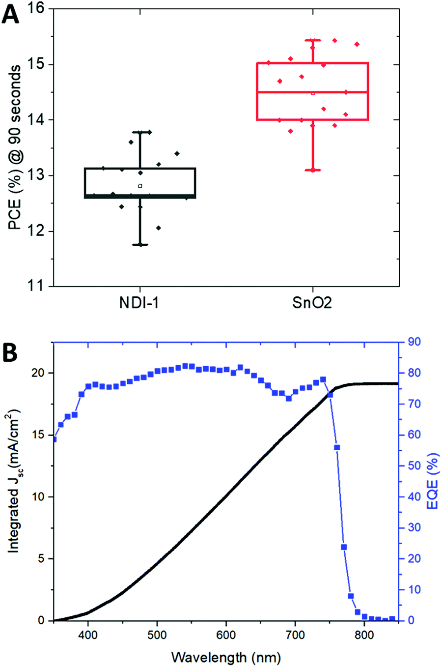 | ||
| Fig. 4 (A) Box plots of the power density of NDI-1 and SnO2 devices and (B) and external quantum efficiency (EQE) and integrated short-circuit current plots for the NDI-1 devices. | ||
Long-term stability
Both NDI-1 and SnO2 based devices were stable for multiple months when stored in a dry box (relative humidity < 5%) in the dark, showing no changes in performance and indicating a high shelf life for the devices. To compare the stability differences between devices employing NDI-1 to their tin oxide counterparts, we encapsulated (see Experimental section) full devices and aged them in an environmental chamber at open circuit voltage at 60 °C, in air. The study was conducted over 290 hours where the tin oxide device efficiency degraded to <10% of the initial value, whereas that of the devices incorporating the NDI-1 polymer retained ca. 35% of the original performance, the degradation being dominated by a loss of FF. Fig. 5 shows the evolution of PCE over aging time for champion and median devices. Although LiTFSI/tBP-doped Spiro-OMeTAD is the common HTM in both devices and has known instabilities that may ultimately limit the stability of the best devices here,43,44 those devices incorporating NDI-1 are more stable over the period of the study.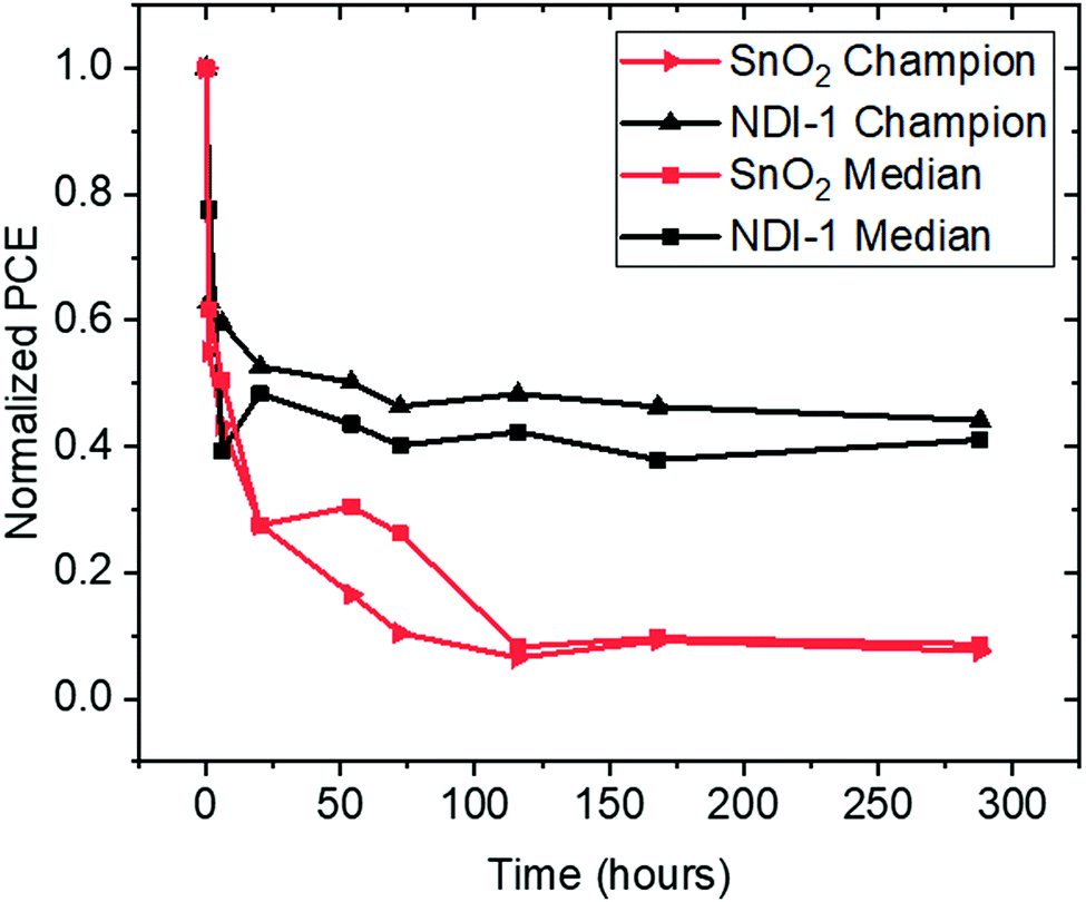 | ||
| Fig. 5 Long term stability of devices employing SnO2 and NDI-1. | ||
Conclusions
We demonstrate in this study a side chain NDI polymer that is superior in performance to several NDI small molecules in n-i-p PSCs. We achieved a champion device with 14% PCE using a undoped films of NDI-1. These devices exhibited greater stability than SnO2-based control devices when aged under 1 sun conditions for almost 300 hours and 60 °C. This provides a foundation for designing other possible naphthalene diimides or other moieties to be used as dopant-free solution-processable electron-transport materials to replace metal oxide ETMs. This low temperature processing route open new avenues for polymer-based flexible solar cells and the optical transparency for incorporation in tandem devices.Materials and methods
Commercially available precursors as well as the solvents were purchased form Sigma Aldrich and used without modifications. Detailed synthetic procedures and characterization data are presented in the ESI.†FTO coated glass slides (1 cm2) were cleaned by sonication in 2% Hellmanax in water, followed by deionized water, and ethanol for 15 min each. The slides were then dried and plasma etched for 10 min and used immediately. Organic ETM solutions were prepared by making 1.5 mg mL−1 solutions in chlorobenzene,45 which were spun at 2000 rpm for 30 s in air yielding layers of 10 nm thickness. When tin oxide was used as an ETM the layer was prepared by spin coating 10 mg mL−1 solution in isopropyl alcohol of SnCl2·5H2O at 2000 rpm for 20 s followed by annealing at 180 °C for 1 h. Plasma treatment for 1 min was done before SnO2 nanoparticles were deposited by diluting commercially available precursor in 1![[thin space (1/6-em)]](https://www.rsc.org/images/entities/char_2009.gif) :10 DI water then spin coating it at 2000 rpm for 20 s followed by annealing at 180 °C for 1 h. Alumina nanoparticles (<50 nm) were dispersed in isopropanol in 1:150 v/v ratio. 100 μL of this dispersion was then dynamically spun onto the ETL at 3000 rpm for 30 s and then dried at 60 °C for 1 min. The perovskite precursor was prepared by mixing 507.1 mg of PbI2, 73.4 mg PbBr2, 22.4 mg MABr, 172 mg FAI, with 41 μL of 1.5 M CsI solution (in DMSO) and 850 μL of a pre-mixed 4:1 DMF:DMSO. The perovskite was then spun using a two-step program by covering the film with 50 μL of the perovskite solution, and spinning that at 1000 rpm for 10 seconds, followed by 6000 rpm for 20 s. When 5 s were left to the end of the program, 260 μL of chlorobenzene was dropped to solvent quench the film. The films were rapidly moved to a hot hotplate to be annealed at 100 °C in the dark for 1 h where they turned black immediately. The Spiro-OMeTAD layer was prepared by preparing a 72 mg mL−1 solution of Spiro-OMeTAD in chlorobenzene followed by the addition of a 17.5 μL LiTFSI solution (52 mg mL−1 concentration in acetonitrile) and 28.8 μL of tBP. The mixed solution was spun dynamically at 2000 rpm for 30 s and devices were exposed to dry air in the dark for doping to take place overnight. Gold electrodes were evaporated using a metal sputter, using a shadow mask to fix the area at 0.16 cm2, and evaporated at 0.1 nm s−1 for the first 10 nm and 1 nm s−1 afterwards.
:10 DI water then spin coating it at 2000 rpm for 20 s followed by annealing at 180 °C for 1 h. Alumina nanoparticles (<50 nm) were dispersed in isopropanol in 1:150 v/v ratio. 100 μL of this dispersion was then dynamically spun onto the ETL at 3000 rpm for 30 s and then dried at 60 °C for 1 min. The perovskite precursor was prepared by mixing 507.1 mg of PbI2, 73.4 mg PbBr2, 22.4 mg MABr, 172 mg FAI, with 41 μL of 1.5 M CsI solution (in DMSO) and 850 μL of a pre-mixed 4:1 DMF:DMSO. The perovskite was then spun using a two-step program by covering the film with 50 μL of the perovskite solution, and spinning that at 1000 rpm for 10 seconds, followed by 6000 rpm for 20 s. When 5 s were left to the end of the program, 260 μL of chlorobenzene was dropped to solvent quench the film. The films were rapidly moved to a hot hotplate to be annealed at 100 °C in the dark for 1 h where they turned black immediately. The Spiro-OMeTAD layer was prepared by preparing a 72 mg mL−1 solution of Spiro-OMeTAD in chlorobenzene followed by the addition of a 17.5 μL LiTFSI solution (52 mg mL−1 concentration in acetonitrile) and 28.8 μL of tBP. The mixed solution was spun dynamically at 2000 rpm for 30 s and devices were exposed to dry air in the dark for doping to take place overnight. Gold electrodes were evaporated using a metal sputter, using a shadow mask to fix the area at 0.16 cm2, and evaporated at 0.1 nm s−1 for the first 10 nm and 1 nm s−1 afterwards.
Devices were measured under 1 sun illumination using a custom-built 16-device set-up in which the devices were light soaked for at least 90 s before measurements to ensure stabilization where the aperture size was fixed at 0.16 cm2. Encapsulation was achieved by dispensing UV-curable epoxy resin from Nagase (XNR5516Z-B1) onto the edges of a cover glass with a recess in the middle. The cover glass was then gently pressed on to the solar cell devices and were illuminated from the cover glass side under UV light.
UV-vis-NIR measurements were done on a Cary 5000 spectrophotometer. PL spectra were done on a Horiba instrument. EQE data were recorded through a Keithley 2400 Source Meter under 300 W xenon lamp irradiation with an Oriel Corner-stone 260¼ m monochromator. The monochromatic photon flux was quantified through a calibrated silicon cell (Peccell Technologies).46 DSC and TGA experiments were performed on Mettler-Toledo TA instruments under nitrogen gas atmosphere and at a scan rate of 10 °C min−1. Gel Premeation Chromatography (GPC) for polymer samples were performed using a Tosoh EcoSEC HLC 8320GPC system with TSKgel SuperHZ-L columns eluting CHCl3 containing 0.25% triethylamine at a flow rate of 0.45 mL min−1. All number-average molecular weights and dispersities were calculated from refractive index chromatograms using PStQuick Mp-M polystyrene standards. Electrochemical measurements were carried out under nitrogen atmosphere with 0.1 M tetra-n-butylammonium hexafluorophosphate in dry dichloromethane using a CH Instruments CHI620D Electrochemical Workstation CHI620D, and a conventional three-electrode cell with a glassy carbon working electrode, platinum wire counter electrode, and an Ag wire coated with AgCl as the pseudo-reference electrode. Potentials were referenced to ferrocenium/ferrocene by using ferrocene as an internal standard. Cyclic voltammograms were recorded at a scan rate of 50 mV s−1.
Conflicts of interest
There are no conflicts to declare.Acknowledgements
This material is based upon work supported by the International Network for Excellence in Photovoltaics, and by the U.S. Department of Energy's Office of Energy Efficiency and Renewable Energy (EERE) under the Solar Energy Technologies Office Award Number DE-EE0008747. D. P. McCarthy acknowledges support from the Department of Education Graduate Assistance in Areas of National Need (GAANN) program at the Georgia Institute of Technology (Award #P200A180075). D. P. McMeekin acknowledges financial support from the Australian Centre for Advanced Photovoltaics. KA acknowledges Dr Boer Tan, and Dr Sonia Ruiz Raga for the helpful discussions.Notes and references
- A. Kojima, K. Teshima, Y. Shirai and T. Miyasaka, Organometal Halide Perovskites as Visible-Light Sensitizers for Photovoltaic Cells, J. Am. Chem. Soc., 2009, 131, 6050–6051 CrossRef CAS.
- C. C. Stoumpos and M. G. Kanatzidis, Halide Perovskites: Poor Man's High-Performance Semiconductors, Adv. Mater., 2016, 28, 5778–5793 CrossRef.
- N. Arora, M. I. Dar, A. Hinderhofer, N. Pellet, F. Schreiber, S. M. Zakeeruddin and M. Grätzel, Perovskite solar cells with CuSCN hole extraction layers yield stabilized efficiencies greater than 20%, Science, 2017, 358, 768–771 CrossRef CAS.
- S. N. Habisreutinger, T. Leijtens, G. E. Eperon, S. D. Stranks, R. J. Nicholas and H. J. Snaith, Carbon Nanotube/Polymer Composites as a Highly Stable Hole Collection Layer in Perovskite Solar Cells, Nano Lett., 2014, 14, 5561–5568 CrossRef CAS.
- M. Saliba, S. Orlandi, T. Matsui, S. Aghazada, M. Cavazzini, J.-P. Correa-Baena, P. Gao, R. Scopelliti, E. Mosconi, K.-H. Dahmen, F. De Angelis, A. Abate, A. Hagfeldt, G. Pozzi, M. Graetzel and M. K. Nazeeruddin, A molecularly engineered hole-transporting material for efficient perovskite solar cells, Nat. Energy, 2016, 1, 15017 CrossRef CAS.
- Z. Zhu, Y. Bai, X. Liu, C.-C. Chueh, S. Yang and A. K. Y. Jen, Enhanced Efficiency and Stability of Inverted Perovskite Solar Cells Using Highly Crystalline SnO2 Nanocrystals as the Robust Electron-Transporting Layer, Adv. Mater., 2016, 28, 6478–6484 CrossRef CAS.
- S. S. Kim, S. Bae and W. H. Jo, A perylene diimide-based non-fullerene acceptor as an electron transporting material for inverted perovskite solar cells, RSC Adv., 2016, 6, 19923–19927 RSC.
- E. H. Anaraki, A. Kermanpur, L. Steier, K. Domanski, T. Matsui, W. Tress, M. Saliba, A. Abate, M. Grätzel, A. Hagfeldt and J.-P. Correa-Baena, Highly efficient and stable planar perovskite solar cells by solution-processed tin oxide, Energy Environ. Sci., 2016, 9, 3128–3134 RSC.
- S. H. Aung, L. Zhao, K. Nonomura, T. Z. Oo, S. M. Zakeeruddin, N. Vlachopoulos, T. Sloboda, S. Svanström, U. B. Cappel, A. Hagfeldt and M. Grätzel, Toward an alternative approach for the preparation of low-temperature titanium dioxide blocking underlayers for perovskite solar cells, J. Mater. Chem. A, 2019, 7, 10729–10738 RSC.
- J. Zhang, Y. Chen and W. Guo, Optimizing the efficiency of perovskite solar cells by a sub-nanometer compact titanium oxide electron transport layer, Nano Energy, 2018, 49, 230–236 CrossRef CAS.
- S. Shi, J. Li, T. Bu, S. Yang, J. Xiao, Y. Peng, W. Li, J. Zhong, Z. Ku, Y.-B. Cheng and F. Huang, Room-temperature synthesized SnO2 electron transport layers for efficient perovskite solar cells, RSC Adv., 2019, 9, 9946–9950 RSC.
- K. Mahmood, S. Sarwar and M. T. Mehran, Current status of electron transport layers in perovskite solar cells: materials and properties, RSC Adv., 2017, 7, 17044–17062 RSC.
- C. Sun, Z. Wu, H.-L. Yip, H. Zhang, X.-F. Jiang, Q. Xue, Z. Hu, Z. Hu, Y. Shen, M. Wang, F. Huang and Y. Cao, Amino-Functionalized Conjugated Polymer as an Efficient Electron Transport Layer for High-Performance Planar-Heterojunction Perovskite Solar Cells, Adv. Energy Mater., 2016, 6, 1501534 CrossRef.
- Z. Zhu, J.-Q. Xu, C.-C. Chueh, H. Liu, Z. A. Li, X. Li, H. Chen and A. K. Y. Jen, A Low-Temperature, Solution-Processable Organic Electron-Transporting Layer Based on Planar Coronene for High-performance Conventional Perovskite Solar Cells, Adv. Mater., 2016, 28, 10786–10793 CrossRef CAS.
- J. Lian, B. Lu, F. Niu, P. Zeng and X. Zhan, Electron-Transport Materials in Perovskite Solar Cells, Small Methods, 2018, 2, 1800082 CrossRef.
- C. Momblona, L. Gil-Escrig, E. Bandiello, E. M. Hutter, M. Sessolo, K. Lederer, J. Blochwitz-Nimoth and H. J. Bolink, Efficient vacuum deposited p-i-n and n-i-p perovskite solar cells employing doped charge transport layers, Energy Environ. Sci., 2016, 9, 3456–3463 RSC.
- K. Wojciechowski, I. Ramirez, T. Gorisse, O. Dautel, R. Dasari, N. Sakai, J. M. Hardigree, S. Song, S. Marder, M. Riede, G. Wantz and H. J. Snaith, Cross-Linkable Fullerene Derivatives for Solution-Processed n-i-p Perovskite Solar Cells, ACS Energy Lett., 2016, 1, 648–653 CrossRef CAS.
- M. Li, Z.-K. Wang, T. Kang, Y. Yang, X. Gao, C.-S. Hsu, Y. Li and L.-S. Liao, Graphdiyne-modified cross-linkable fullerene as an efficient electron-transporting layer in organometal halide perovskite solar cells, Nano Energy, 2018, 43, 47–54 CrossRef CAS.
- F. Pulvirenti, B. Wegner, N. K. Noel, G. Mazzotta, R. Hill, J. B. Patel, L. M. Herz, M. B. Johnston, M. K. Riede, H. J. Snaith, N. Koch, S. Barlow and S. R. Marder, Modification of the fluorinated tin oxide/electron-transporting material interface by a strong reductant and its effect on perovskite solar cell efficiency, Mol. Syst. Des. Eng., 2018, 3, 741–747 RSC.
- D. Zou, F. Yang, Q. Zhuang, M. Zhu, Y. Chen, G. You, Z. Lin, H. Zhen and Q. Ling, Perylene Diimide-Based Electron-Transporting Material forPerovskite Solar Cells with Undoped Poly(3-hexylthiophene) as Hole-Transporting Material, ChemSusChem, 2019, 12, 1155–1161 CrossRef CAS.
- M. Zhang, T. Li, G. Zheng, L. Li, M. Qin, S. Zhang, H. Zhou and X. Zhan, An amino-substituted perylene diimide polymer for conventional perovskite solar cells, Mater. Chem. Front., 2017, 1, 2078–2084 RSC.
- W. Yan, Z. Wang, Y. Gong, S. Guo, J. Jiang, J. Chen, C. Tang, R. Xia, W. Huang and H. Xin, Naphthalene-diimide selenophene copolymers as efficient solution-processable electron-transporting material for perovskite solar cells, Org. Electron., 2019, 67, 208–214 CrossRef CAS.
- W. Liu, D. B. Shaikh, P. S. Rao, R. S. Bhosale, A. A. Said, A. M. Mak, Z. Wang, M. Zhao, W. Gao, B. Chen, Y. M. Lam, W. Fan, S. V. Bhosale, S. V. Bhosale and Q. Zhang, Molecular Aggregation of Naphthalene Diimide(NDI) Derivatives in Electron Transport Layers of Inverted Perovskite Solar Cells and Their Influence on the Device Performance, Chem. – Asian J., 2020, 15, 112–121 CrossRef CAS.
- S.-K. Jung, J. H. Heo, D. W. Lee, S.-C. Lee, S.-H. Lee, W. Yoon, H. Yun, S. H. Im, J. H. Kim and O.-P. Kwon, Nonfullerene Electron Transporting Material Based on Naphthalene Diimide Small Molecule for Highly Stable Perovskite Solar Cells with Efficiency Exceeding 20%, Adv. Funct. Mater., 2018, 28, 1800346 CrossRef.
- T. Jia, C. Sun, R. Xu, Z. Chen, Q. Yin, Y. Jin, H.-L. Yip, F. Huang and Y. Cao, Naphthalene Diimide Based n-Type Conjugated Polymers as Efficient Cathode Interfacial Materials for Polymer and Perovskite Solar Cells, ACS Appl. Mater. Interfaces, 2017, 9, 36070–36081 CrossRef CAS.
- T. Nakamura, N. Shioya, T. Shimoaka, R. Nishikubo, T. Hasegawa, A. Saeki, Y. Murata, R. Murdey and A. Wakamiya, Molecular Orientation Change in Naphthalene Diimide Thin Films Induced by Removal of Thermally Cleavable Substituents, Chem. Mater., 2019, 31, 1729–1737 CrossRef CAS.
- Z. Zhu, J.-Q. Xu, C.-C. Chueh, H. Liu, Z. A. Li, X. Li, H. Chen and A. K.-Y. Jen, A Low-Temperature, Solution-Processable Organic Electron-Transporting Layer Based on Planar Coronene for High-performance Conventional Perovskite Solar Cells, Adv. Mater., 2016, 28, 10786–10793 CrossRef CAS.
- W. Hou, Y. Xiao, G. Han and J.-Y. Lin, The Applications of Polymers in Solar Cells: A Review, Polymers, 2019, 11, 143 CrossRef.
- X. Liu, Y. Cheng, C. Liu, T. Zhang, N. Zhang, S. Zhang, J. Chen, Q. Xu, J. Ouyang and H. Gong, 20.7% highly reproducible inverted planar perovskite solar cells with enhanced fill factor and eliminated hysteresis, Energy Environ. Sci., 2019, 12, 1622–1633 RSC.
- Z. Z. Safari M. B., A. Giuri, F. Bisconti, S. Carallo, A. Listorti, C. Esposito Corcione, M. R. Nateghi, A. Rizzo and S. Colella, Optimizing the Interface between Hole Transporting Material and Nanocomposite for Highly Efficient Perovskite Solar Cells, Nanomaterials, 2019, 11, 143 Search PubMed.
- Y. Zhang, M. Elawad, Z. Yu, X. Jiang, J. Lai and L. Sun, Enhanced performance of perovskite solar cells with P3HT hole-transporting materials via molecular p-type doping, RSC Adv., 2016, 6, 108888–108895 RSC.
- W. Wang, J. Yuan, G. Shi, X. Zhu, S. Shi, Z. Liu, L. Han, H.-Q. Wang and W. Ma, Inverted Planar Heterojunction Perovskite Solar Cells Employing Polymer as the Electron Conductor, ACS Appl. Mater. Interfaces, 2015, 7, 3994–3999 CrossRef CAS.
- E. A. B. Kantchev, H. S. Tan, T. B. Norsten and M. B. Sullivan, O,O′-Disubstituted N,N′-Dihydroxynaphthalenediimides (DHNDI): First Principles Designed Organic Building Blocks for Materials Science, Org. Lett., 2011, 13, 5432–5435 CrossRef CAS.
- L. Echegoyen and L. E. Echegoyen, Electrochemistry of fullerenes and their derivatives, Acc. Chem. Res., 1998, 31, 593–601 CrossRef CAS.
- L. Y. Botero, E. J. López-Rendón, D. Ramírez, M. D. Zapata and F. Jaramillo, From Clay Minerals to Al2O3 Nanoparticles: Synthesis and Colloidal Stabilization for Optoelectronic Applications, Minerals, 2020, 10 Search PubMed.
- D. Ramirez, K. Schutt, J. F. Montoya, S. Mesa, J. Lim, H. J. Snaith and F. Jaramillo, Meso-Superstructured Perovskite Solar Cells: Revealing the Role of the Mesoporous Layer, J. Phys. Chem. C, 2018, 122, 21239–21247 CrossRef CAS.
- D. Ramirez, E. Velilla, J. F. Montoya and F. Jaramillo, Mitigating scalability issues of perovskite photovoltaic technology through a p-i-n meso-superstructured solar cell architecture, Sol. Energy Mater. Sol. Cells, 2019, 195, 191–197 CrossRef CAS.
- D. Wang, Q. Chen, H. Mo, J. Jacobs, A. Thomas and Z. Liu, A bilayer TiO2/Al2O3 as the mesoporous scaffold for enhanced air stability of ambient-processed perovskite solar cells, Mater. Adv., 2020, 1, 2057–2067 RSC.
- M. Saliba, T. Matsui, J.-Y. Seo, K. Domanski, J.-P. Correa-Baena, M. K. Nazeeruddin, S. M. Zakeeruddin, W. Tress, A. Abate, A. Hagfeldt and M. Grätzel, Cesium-containing triple cation perovskite solar cells: improved stability, reproducibility and high efficiency, Energy Environ. Sci., 2016, 9, 1989–1997 RSC.
- N. J. Jeon, J. H. Noh, Y. C. Kim, W. S. Yang, S. Ryu and S. I. Seok, Solvent engineering for high-performance inorganic–organic hybrid perovskite solar cells, Nat. Mater., 2014, 13, 897–903 CrossRef CAS.
- We note that the use of chlorobenzene might lead to some dissolution of small quantities of ETL, although the alumina interlayer likely offers some protection. However, small quantities may play a role in passivating perovskite grain boundaries, as described for other ester-containing polymers (e.g. poly(methylmethacrylate) in ref. 42). In the case of the small molecules DMF may also cause some dissolution of the ETM (see Fig. S9, ESI†).
- D. Bi, C. Yi, J. Luo, J.-D. Décoppet, F. Zhang, S. M. Zakeeruddin, X. Li, A. Hagfeldt and M. Grätzel, Polymer-templated nucleation and crystal growth of perovskite films for solar cells with efficiency greater than 21%, Nat. Energy, 2016, 1, 16142 CrossRef CAS.
- C. C. Boyd, R. Cheacharoen, T. Leijtens and M. D. McGehee, Understanding Degradation Mechanisms and Improving Stability of Perovskite Photovoltaics, Chem. Rev., 2019, 119, 3418–3451 CrossRef CAS.
- The reference (SnO2) devices give slightly lower device performance than expected; there are many possible causes, but small variations in humidity and O2 levels during fabrication may play a role.
- Concentrations in the range 0.5–5.0 mg mL−1 were tried; however, the most efficient devices were obtained for concentrations of ca. 1.5 mg mL−1, which corresponded to film thicknesses of ca. 10 nm.
- Small inconsistencies in JSC between the integrated EQE data and the J–V data may result from imperfect EQE calibration.
Footnote |
| † Electronic supplementary information (ESI) available. See DOI: 10.1039/d0qm00685h |
| This journal is © the Partner Organisations 2021 |