
 Open Access Article
 This Open Access Article is licensed under a
 Creative Commons Attribution 3.0 Unported Licence
Imaging atomic motion of light elements in 2D materials with 30 kV electron microscopy†
Sytze
de Graaf
 *a,
Majid
Ahmadi
a,
Ivan
Lazić
b,
Eric G. T.
Bosch
b and
Bart J.
Kooi
*a
*a,
Majid
Ahmadi
a,
Ivan
Lazić
b,
Eric G. T.
Bosch
b and
Bart J.
Kooi
*a
aZernike Institute for Advanced Materials, University of Groningen, Nijenborgh 4, 9747 AG Groningen, The Netherlands. E-mail: sytze.de.graaf@rug.nl; b.j.kooi@rug.nl
bThermo Fisher Scientific, Achtseweg Noord 5, 5651 GG Eindhoven, The Netherlands
First published on 30th November 2021
Abstract
Scanning transmission electron microscopy (STEM) is the most widespread adopted tool for atomic scale characterization of two-dimensional (2D) materials. However, damage free imaging of 2D materials with electrons has remained problematic even with powerful low-voltage 60 kV-microscopes. An additional challenge is the observation of light elements in combination with heavy elements, particularly when recording fast dynamical phenomena. Here, we demonstrate that 2D WS2 suffers from electron radiation damage during 30 kV-STEM imaging, and we capture beam-induced defect dynamics in real-time by atomic electrostatic potential imaging using integrated differential phase contrast (iDPC)-STEM. The fast imaging of atomic electrostatic potentials with iDPC-STEM reveals the presence and motion of single sulfur atoms near defects and edges in WS2 that are otherwise invisible at the same imaging dose at 30 kV with conventional annular dark-field STEM, and has a vast speed and data processing advantage over electron detector camera based STEM techniques like electron ptychography.
Introduction
Two-dimensional materials are a hot topic of research for their large potential in future applications by virtue of their reduced dimensions and tunable properties. Also, novel properties can emerge that are not present in the bulk. Semiconducting transition metal dichalcogenides (TMDs) are among the most extensively investigated 2D materials, and have found their use in various fields such as spintronics,1 neuromorphics,2 optoelectronics,3 sensing4 and catalysis.5Scanning transmission electron microscopy is the most popular tool for the direct observation of crystalline structures, grain boundaries and defects of 2D materials that contribute to their macroscopic properties. Moreover, STEM is the only available tool capable of (sub) nanometer sculpting e.g. to create nanometer sized holes for DNA sequencing,6 and for the manipulation of single atoms.7,8 Another major advantage of scanning an electron probe (with STEM) over parallel electron wave illumination (with TEM), is the ability to simultaneously employ multiple electron detectors for imaging as well as for spectroscopy purposes, such that atomically resolved images and chemical maps can be acquired simultaneously. Also, direct control of resolution and depth-of-focus is possible with STEM and not with TEM.9–12 Moreover, the interpretation of atomic resolution STEM images is generally also more straightforward, since atoms may appear white or black when deviating from perfect focus with TEM, although this can be largely resolved with extra aberration correction hardware.13
The development of low-voltage aberration corrected microscopes has been crucial for the (largely) damage free imaging of 2D materials. Nowadays, modern microscopes operating at 60 kV are widely and routinely used to image 2D materials with atomic resolution. Although radiation damage of pristine graphene is then fully prevented, defects in graphene and insulating and semiconducting 2D materials remain susceptible to radiation damage despite the milder imaging conditions. In an effort to further understand and potentially reduce radiation damage, state-of-the-art S/TEM systems have been developed in recent years, operating at low-voltages of 30 kV,14,15 20 kV (ref. 16) and even 15 kV.17,18 Where particular the SALVE microscope has been leading the electron radiation damage research by atomic resolution low-voltage TEM imaging of various 2D materials.13,16,19–21 However, specifically these low-voltage STEM systems have only demonstrated real atomic resolution on graphene and not on any other 2D materials, leaving the investigations of semiconducting 2D materials like TMDs and the electron–matter interactions with low-voltage STEM unexplored.
Enhancing imaging sensitivity is as important as pushing the imaging resolution at reduced voltages, i.e. resolution is useless without contrast. Emerging techniques such as integrated differential phase contrast (iDPC)-STEM22,23 and the recently demonstrated super-resolution electron ptychography24,25 are capable of reaching substantially higher sensitivity than the conventional annular dark-field (ADF)-STEM. With this latter technique, relatively light elements are invisible or have reduced contrast, possibly below the noise level, as it images the square of the electrostatic potential,9,23 providing nearly atomic number squared (Z1.6–2.0) contrast.26 On the other hand, iDPC-STEM and electron ptychography are capable of atomic electrostatic potential imaging, which is about linear in Z.22,24,25,27 This substantially improves sensitivity as we have recently demonstrated by the direct imaging of hydrogen atoms in titanium hydride using iDPC-STEM.28
Observing dynamical phenomena, like phase transitions or single atom motion, is generally more valuable for the fundamental understanding of materials than single snapshots of static materials. However, such experiments require a STEM imaging technique that is both sensitive and fast, which to date has not been demonstrated.
Here we observe beam-induced radiation damage and defect dynamics in semiconducting 2D WS2 by recording atomic electrostatic potential movies with iDPC-STEM using a primary electron energy of 30 keV. Imaging with iDPC-STEM enables the use of lower electron doses or higher framerates relative to conventional STEM techniques, and produces electrostatic potential images in real-time during acquisition. WS2 is a member of the family of TMDs, which have a characteristic layered structure that is easily separable into their monolayer constituents by virtue of the weak interlayer van der Waals forces. The intralayer forces have a mixed covalent-ionic nature and the monolayer consists of a plane of tungsten (W) atoms that is sandwiched between two planes of sulfur (S) atoms. In the WS2 that we study here, the W atoms are trigonal prismatically coordinated (2H structure) with six S atoms, rendering the WS2 monolayer a direct semiconductor. The S atoms overlap when viewed perpendicular to the plane as a result of the trigonal prismatic coordination. The projected atomic number of W and the two S atom stack (which we refer to as S2) is Z = 74 and Z = 32, respectively. A single sulfur vacancy (VS) has a projected atomic number of Z = 16, and a single tungsten vacancy (VW) or a double sulfur vacancy (V2S) yields a local vacuum. The relatively large contrast in projected atomic number is the rationale for using here an atomic electrostatic potential imaging technique.
Experimental
Monolayer parts of 2H WS2 were exfoliated from a bulk single crystal (HQ Graphene) using the scotch tape method, and also grown directly on a silicon wafer using chemical vapor deposition. The 2D WS2 flakes were identified using optical microscopy and transferred to a Quantifoil TEM grid using a polymer free method. A double aberration corrected 30–300 kV Thermo Fisher Scientific Themis Z S/TEM operating at 30 kV was used to image 2D WS2 with atomic resolution. Geometrical and chromatic aberrations were minimized by careful alignment of the probe corrector, and by excitation of the monochromator, respectively. The probe convergence semi-angle was 33 mrad, the probe current 2.5–7.5 pA (depending on energy selecting aperture size), probe step size 15.92–22.52 pm, and the dwell time 40–50 μs. The collection angles of the segmented DF4 detector (for iDPC-STEM imaging) and ADF detector were 9–36 mrad and 39–200 mrad, respectively. Detailed information on the sample preparation and the electron microscopy acquisition can be found in the ESI.† The data is available at the University of Groningen data repository.29Results and discussion
In Fig. 1 we compare simultaneously acquired atomic resolution iDPC-STEM and ADF-STEM images of a 2H WS2 monolayer. The two selected regions (Fig. 1a–d and e–h) contain various elements and defects: W, S2, VW, VS and V2S. All of these features are present in the atomic electrostatic potential images captured using iDPC-STEM, with clearly distinguishable contrast between S2, VS and V2S, matching quantitatively with image simulations (ESI, Fig. S2†). The ADF-STEM images also contain signals from both W and S2, however, without appreciable contrast between S2, VS and V2S. The intensity line profiles shown in Fig. 1i and j quantify the critical improvement in sensitivity of iDPC-STEM compared to ADF-STEM to detect all atoms and defects present.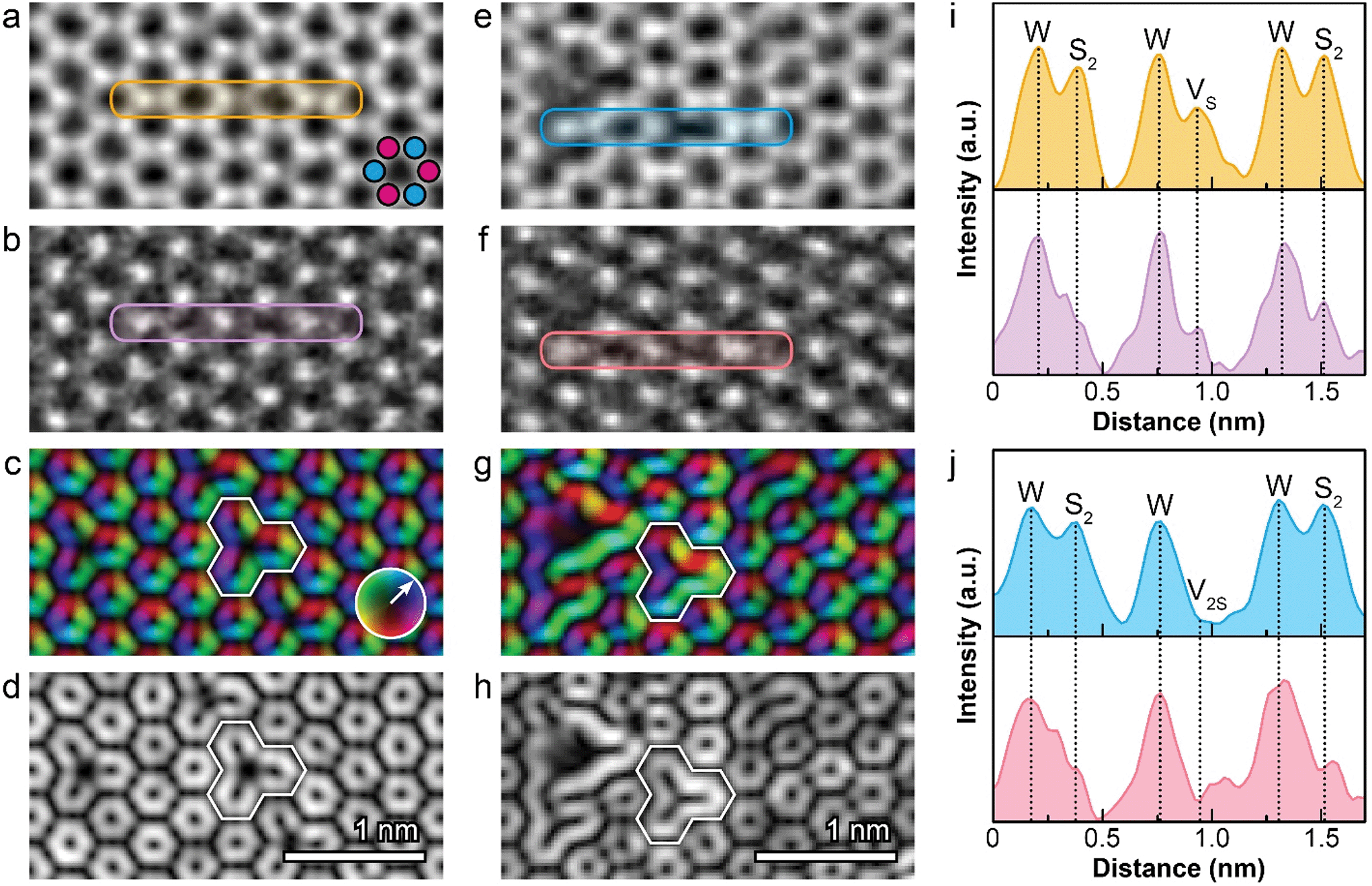 | ||
| Fig. 1 Atomically resolved experimental 30 kV-STEM images of a 2H WS2 monolayer with single (VS) and a double (V2S) sulfur vacancies. Simultaneously acquired images of two regions with different defects are shown in (a–d) and (e–h). The images in (a–d) and (e–h) are, from top to bottom: electrostatic potential (iDPC-STEM), square of the electrostatic potential (ADF-STEM), electric vector field (DPC-STEM) and magnitude of electric field (magnitude of DPC-STEM). The lower image quality of (e–h) is caused by a combination of crystal misalignment and minor residual low-order aberrations, which is particularly visible by the reduced sulfur atom signal in the ADF-STEM image. Line profiles of W, S2, VS and V2S are extracted from the marked rectangles in the iDPC-STEM (a, e) and ADF-STEM (b, f) images and are plotted in (i, j). The WS2 schematic in (a) indicates the position of W and S2 with magenta and cyan dots, respectively, and applies to all images. The VS and V2S defects are indicated in (c, d) and (g, h). Field strength in (c, g) is represented according to the color wheel inset in (c). | ||
The atomic electric field is displayed as a (colorized) vector field and vector magnitude image in Fig. 1c, d and g, h. These images are two different representations of the same differential phase contrast (DPC)-STEM vector image that is complementing the atomic electrostatic potential (iDPC-STEM) scalar image.22,27,30 In these images, nodes exist at positions where the projected electric field is zero. This occurs at high-symmetry points where the electric field cancels out i.e. at the atom positions, bridge sites and hollow sites. Anomalies such as VS and V2S are readily detected by their distinct shape in atomic electric field images as outlined in Fig. 1c, d, g and h. Moreover, the sulfur atoms and its vacancies remain detectable even when the WS2 is tilted a few degrees with respect to the electron beam optical axis (ESI Fig. S3†). Hence, both atomic electrostatic potentials and atomic electric fields, which are retrieved from the same detector data, have robust single atom sensitivity and are a powerful method to detect light elements.
We observe the formation of point defects, defect complexes and agglomerates, one-dimensional (1D) defects and holes under influence of the 30 keV electron beam (Movies S1–S3†). To capture these dynamics with a large field of view and a practically useful framerate (e.g. 10–20 seconds per frame of a 10 × 10 nm2 area), a lower effective electron dose than in Fig. 1 has to be used. The five times lower electron dose (from 7.4 × 10⁴ e Å−2 to 1.5 × 10⁴ e Å−2, see ESI†) typically causes loss of signal from the light elements such as S2 and S in the ADF-STEM images, such that then only contrast from W remains (ESI Fig. S5–S7†). This is not the case for the atomic electrostatic potential image where all features remain detectable, as has been demonstrated with ultralow-dose imaging of zeolites23,31 and metal–organic frameworks,32 due to the intrinsic high sensitivity and noise suppression property of iDPC-STEM.22,23
We first show the creation and dynamics of VW, VS and V2S point defects by four subsequent frames in Fig. 2. The defects present are schematically indicated in the electric field magnitude images Fig. 2e–h. The time interval between the frames is in this case 14.0 seconds, but these frames were cut from a larger overview and the actual time to record each field of view shown was 1.0 second. In the first frame, VS and V2S are randomly distributed, which agglomerate in the second frame. Hence, the point defects are mobilized under influence of the 30 keV electron beam. The defects are particularly visible in the electric field and atomic electrostatic potential images but are practically invisible in the ADF-STEM image. The third frame shows that a W atom, originally residing at the center of the sulfur vacancy agglomerate, has moved about 1 nm to a W–W bridge position. The ejected W atom was likely destabilized due to undercoordination at its original position in the sulfur defect agglomerate. Finally, in the fourth frame the W atom has moved back to its original site and sulfur defects have lined up to create a 1D sulfur vacancy line (SVL).33,34 Note that this process is largely invisible in the ADF-STEM image, except for the short moment (single frame) the tungsten vacancy is present.
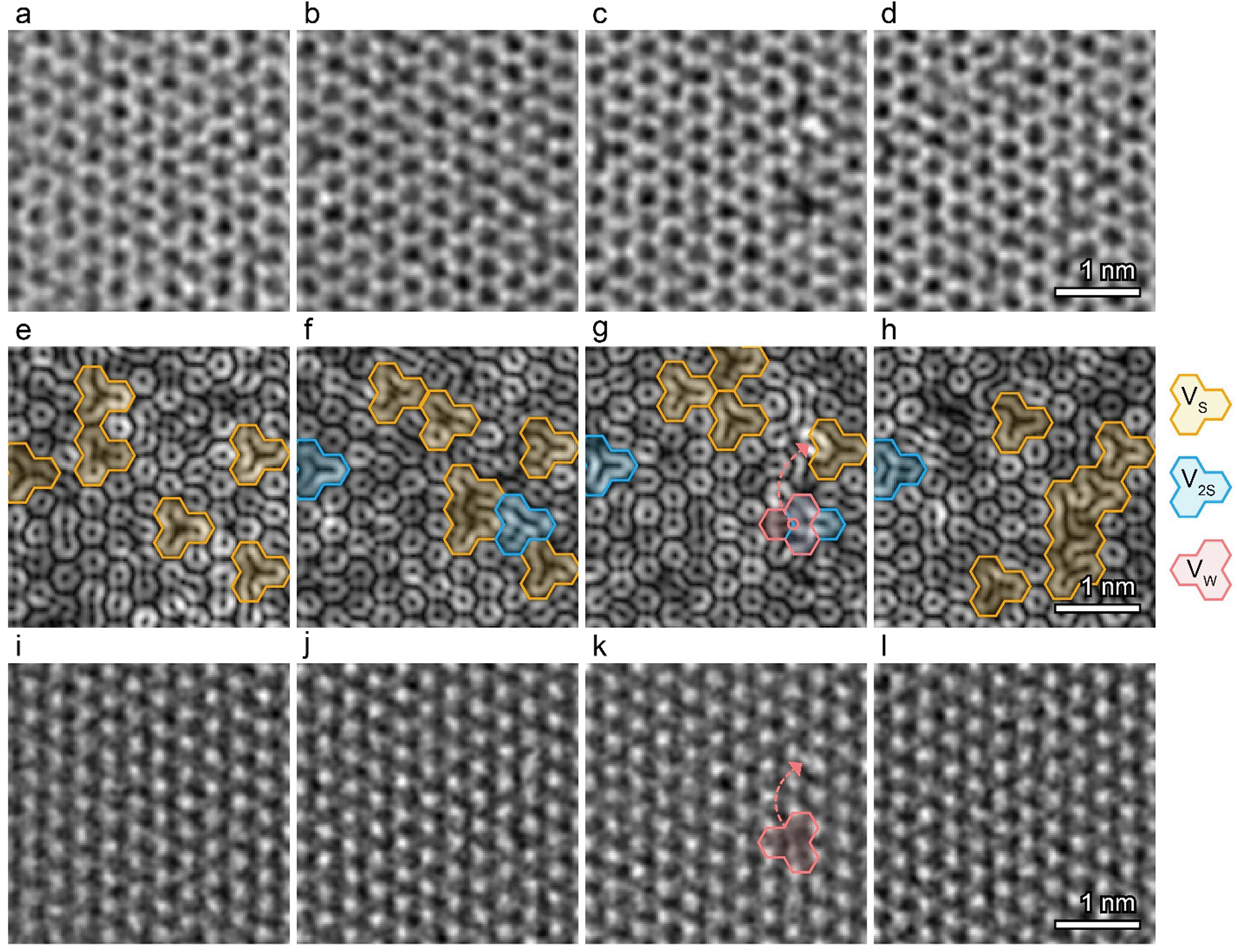 | ||
| Fig. 2 Four frame sequence displaying point defect creation and motion induced by the 30 keV electron beam. The rows display simultaneously acquired images of the electrostatic potential (iDPC-STEM) (a–d), electric field magnitude (DPC-STEM) (e–h), and square of the electrostatic potential (ADF-STEM) (i–l). The defects present are schematically indicated in the electric field magnitude images. | ||
We observed that formation of SVLs is the dominant mechanism to accommodate sulfur vacancies in WS2 upon exposure to the 30 keV electron beam, similar to what has been observed for MoS2 with an electron beam energy of 60 keV or when the specimen is heated to elevated temperatures.20,35,36 An example of this process is shown in Fig. 3, where the same area as in Fig. 2 is presented, but 15 frames later.
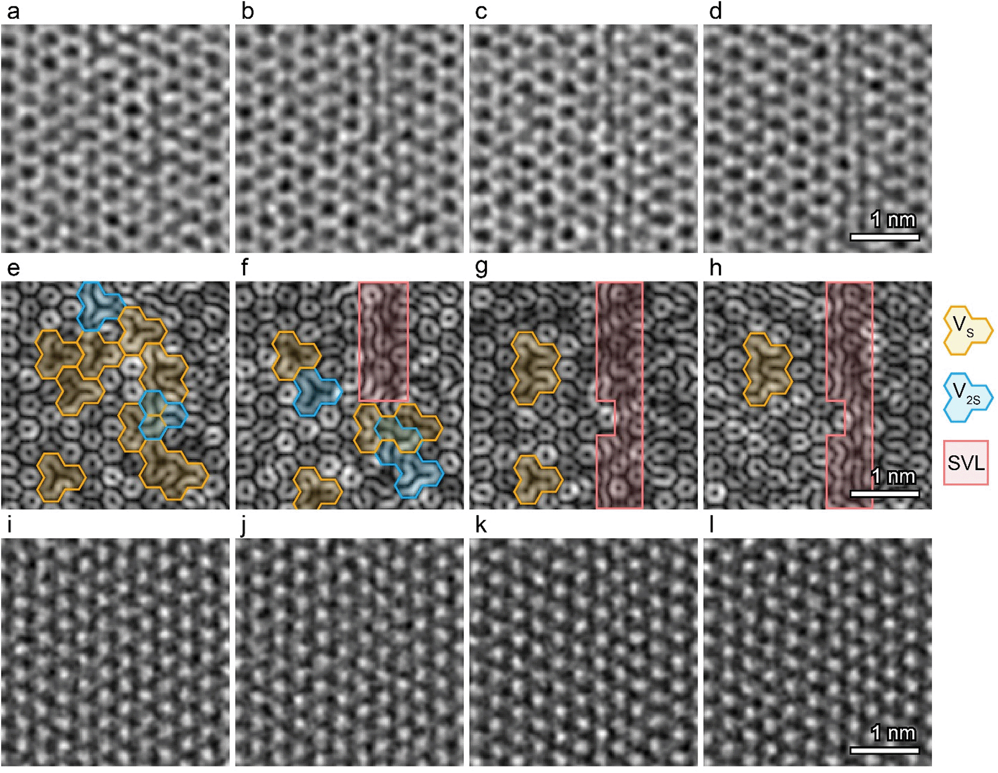 | ||
| Fig. 3 Four frame sequence showing how point defects agglomerate into line defects induced by the 30 keV electron beam. The columns display simultaneously acquired images of the electrostatic potential (iDPC-STEM) (a–d), electric field magnitude (DPC-STEM) (e–h), and square of the electrostatic potential (ADF-STEM) (i–l). The defects present are schematically indicated in the electric field magnitude images. | ||
Holes are created as well in WS2 after prolonged exposure (nearly 50 frames after Fig. 3) to the 30 keV electron beam. Prior to this, the WS2 is in a highly defective state with a high density of point defects and SVLs. Further exposure first leads to loss of W atoms and is then (within several frames) followed by rapidly growing holes. We observe single atom motion at the exposed hole edges, of which the dynamics at W-terminated zigzag edges are displayed in Fig. 4.
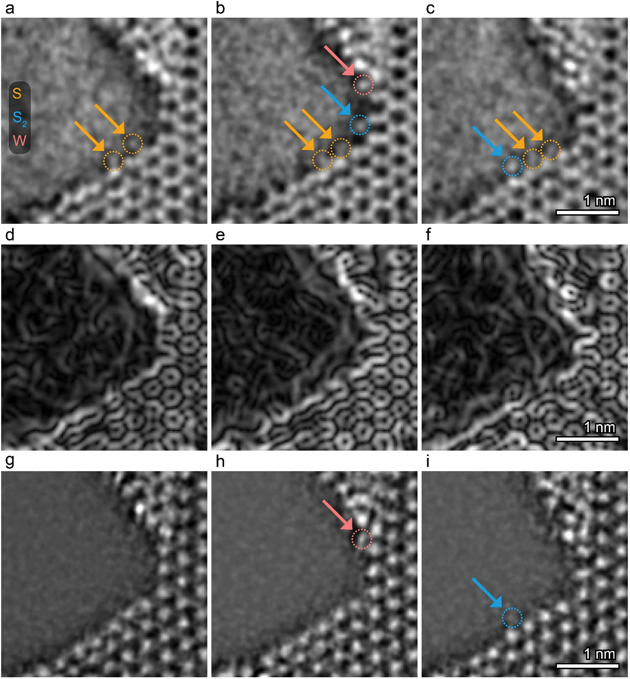 | ||
| Fig. 4 Sequence of frames revealing single atom motion at WS2 edges induced by the 30 keV electron beam. The rows display simultaneously acquired images of the atomic electrostatic potential (iDPC-STEM) (a–c), atomic electric field magnitude (DPC-STEM) (d–f), and square of the electrostatic potential (ADF-STEM) (g–i). Colored arrows point at specific edge atoms present. | ||
The two edges are both terminated by W atoms, but they have a different symmetry, because one of the edges is a true W-terminated zigzag edge (diagonal edge), whereas the other edge (vertical edge) was originally an S-terminated edge, where the S atoms have been removed by the electron beam. Here we show how W and S atoms are appearing at the edges and bond to exposed undercoordinated W edge atoms. This is evident beyond any doubt in the atomic electrostatic potential images (see also Fig. S8†), and just noticeable in the electric field images as well, although more difficult to interpret if the latter would have to stand alone. In contrast, in the ADF-STEM image only the W atom is robustly visible, and a lot of atomic structure details are thus missing.
Attaining atomic resolution with 30 keV electrons is fundamentally more challenging than using more conservative energies of 60 keV and 80 keV, because the resolution is proportionally limited by the electron wavelength, which, at 30 keV, is longer by about 43% and 67% compared to 60 and 80 keV, respectively. To achieve atomic resolution with the longer wavelength, advanced and highly-stable geometrical aberration correctors are required that enable the increase of the numerical aperture of the probe forming lens (see ESI†). In addition, a more monochromatic electron beam is necessary to minimize probe broadening due to chromatic aberrations. This can be achieved with a cold field-emission electron gun or an electron monochromator as we use here, which limits the available electron dose and thus demands the use of a dose efficient imaging technique such as iDPC-STEM.
The strong efforts in the last decade to achieve atomic resolution at accelerating voltages much lower than the traditional 200 and 300 kV were strongly motivated by prospects of reduced electron beam damage allowing materials to be studied in their intrinsic state for prolonged times. Indeed, the knock-on displacement damage is greatly reduced when lowering the accelerating voltage to 80 or 60 kV. In particular for carbon-based materials, like carbon nanotubes and graphene, this development towards lower accelerating voltages has been very successful. However, caution is required since damage by other mechanisms, in particular radiolysis, aggravate for less conductive materials such as semiconductors and insulators.
The active radiation damage mechanisms for semiconducting 2D materials have only been experimentally investigated using low-voltage TEM. Such experiments have recently uncovered a possible new two-step damage mechanism that is only activated at ultralow electron beam energies: long lived electronic excitations may enable knock-on damage when electrons arrive at a sufficiently high rate, which were previously considered to be independent physical processes.21 However, since the energy delivery process by the electron beam is different for STEM compared to TEM, with local illumination, substantially higher dose rates, lower beam current, longer time between impinging electrons and sequential scanning, also different radiation damage mechanisms may be active, such that it is crucial to investigate the radiation damage of semiconducting 2D materials using also 30 kV-STEM.
The present results show that the 2D WS2 analyzed here is not inert to the 30 keV electron beam. Sulfur vacancies are readily created, and they diffuse through the material as is evident from the formation of SVLs. The mechanisms that provide energy for such processes must be dominantly related to ionization effects and to a much lesser extent knock-on displacement. In particular, the ionization cross-section increases with decreasing electron beam energy and is more profound in semiconducting materials (which is the case here for the 2H WS2).37,38 On the other hand, 30 keV is well below the knock-on displacement threshold of S and W, since, respectively, only about 2.1 eV and 370 meV is transferred upon head-on collision of the primary 30 keV electron beam with the atom nuclei.39 A comparison with 60 keV for the same WS2 material shows that the dynamics of damage formation is rather different for 30 and 60 kV, even worsening the situation at the lower accelerating voltage. Results of this comparison are presented in a follow-up paper.40 More in general, the electron beam damage mechanisms at play at these low beam energies are not fully understood, and remain an active area of research.21,41
The ability to image atomic electrostatic potentials of 2D WS2 with high framerate at 30 kV is an improvement over the previously reported 30 kV ADF-STEM image of graphene.14 Mainly due to the fact that graphene is not susceptible to beam damage at these low voltages, such image quality can be improved by increasing the electron dose. The 2D WS2 that we study here, however, is sensitive to ionization damage and directly restricts the electron dose. We have demonstrated that the image quality of ADF-STEM deteriorates under these conditions, whereas atomic electrostatic potential imaging remains of high quality due to the inherent high sensitivity and noise suppression property of iDPC-STEM.
Consequently, capturing the atomic electrostatic potential image with high framerate is not only possible from an image quality perspective, but also from a technical perspective, because iDPC-STEM employs solid-state electron detectors that have equivalent readout speeds to, for example, ADF detectors. In the iDPC-STEM images, however, the contrast between W and S2 is limited, such that the combination of the ADF-STEM and iDPC-STEM image is still necessary to differentiate between them. There are two reasons that contribute to this effect. The dominant contribution is of fundamental nature: the finite resolution of the electron microscope bandwidth limits the potential from W atoms more strongly than the S atoms,42 reducing the contrast of IW/IS2 from about 1.8 to 1.25. The other smaller contribution is the finite accuracy of iDPC-STEM to image atomic electrostatic potentials, which increases the relative intensity of S compared to W (see ESI and Fig. S4†).
Atomic electrostatic potential imaging can be achieved with absolute accuracy with electron ptychography, or when truly integrated center-of-mass (iCOM)-STEM imaging is performed,22,23 which is only approximated (although rather well with even only four detector segments) by iDPC-STEM. The advantage of electron ptychography is that it can further improve contrast with its super-resolution capabilities. However, iDPC-STEM is considerably more suitable for dynamical phenomena studies than electron ptychography, due to its direct imaging and vast speed advantage, because the several solid-state electron detectors that iDPC-STEM employs are two to three orders of magnitude faster than electron detecting cameras used for electron ptychography and 4D STEM, although the speed of such camera detectors are expected to improve in the near future.43,44 For instance, four image frames of 512 × 512 pixels are acquired in about 1 minute with iDPC-STEM in this work (and up to 100 times higher frame rates are readily possible), but take at least 35 minutes with 4D STEM, which additionally produce large datasets (68 GB versus 17 MB for iDPC-STEM) and require time consuming and complex reconstructions schemes for electron ptychography.24,25,45 We note, however, that even the fastest iDPC-STEM acquisition of a reasonable field-of-view is limited to a frame time of 0.1–1.0 second, by no means fast enough for many physical phenomena occurring on shorter timescales. Nevertheless, the fact that iDPC-STEM is not intrinsically limited by the readout speed of the detectors, but rather the electron dose, is promising for potential high-speed imaging capabilities when instrumental advancements enable much higher electron dose rate. Moreover, the accuracy of iDPC-STEM can be readily improved, approaching the absolute accuracy of iCOM-STEM, by employing more solid-state electron detectors than the four that we use here, without compromising speed.
Furthermore, simultaneous imaging and electron energy loss spectroscopy (EELS) cannot be performed with electron ptychography, because all electrons are blocked by the camera, although recently the idea of performing electron ptychography using a camera with a central hole has been reported.46 iDPC-STEM is directly compatible with EELS, as its detector already has a central hole. This is of particular importance considering the advent of ultra-high energy resolution EELS,47 and fast and sensitive direct electron detectors for EELS48 that are opening up new fields in electron microscopy e.g. the ability to directly measure vibrational spectra to investigate phonon modes in nanostructured materials at atomic resolution.49–52
Conclusions
In summary, we have demonstrated that defect dynamics in 2D WS2 can be imaged with enhanced sensitivity and high framerates using the low electron beam energy of 30 keV. This has been enabled by the atomic electrostatic potential imaging capability of iDPC-STEM and advancements in electron optics. At present, this is the only STEM imaging technique that combines high sensitivity and high framerates. The real-time iDPC-STEM movies reveal light sulfur atoms and their dynamics in WS2 that are invisible with the traditional ADF-STEM. This approach can be directly applied to visualize light elements, like oxygen, carbon and nitrogen, next to heavy ones in all 2D materials, and can be generalized to all other beam sensitive materials that require low electron dose and low beam energies. The possibility of combining this fast and sensitive imaging technique with powerful emerging electron spectroscopic capabilities has the potential to solve challenging problems in materials science.Conflicts of interest
E. G. T. B. and I. L. are employees of Thermo Fisher Scientific. The other authors declare no competing interests.Acknowledgements
Financial support from the Zernike Institute for Advanced Materials and the Groningen Cognitive Systems and Materials Center is gratefully acknowledged. T. S. Ghiasi, J. Peiro, A. Kaverzin are thanked for all their time and support in TEM specimen preparation. M. Liang is acknowledged for the CVD grown WS2.References
- N. Tombros, C. Jozsa, M. Popinciuc, H. T. Jonkman and B. J. van Wees, Electronic spin transport and spin precession in single graphene layers at room temperature, Nature, 2007, 448, 571–574 CrossRef CAS PubMed.
- X. Zhu, D. Li, X. Liang and W. D. Lu, Ionic modulation and ionic coupling effects in MoS 2 devices for neuromorphic computing, Nat. Mater., 2019, 18, 141–148 CrossRef CAS PubMed.
- K. F. Mak and J. Shan, Photonics and optoelectronics of 2D semiconductor transition metal dichalcogenides, Nat. Photonics, 2016, 10, 216–226 CrossRef CAS.
- J. Ping, Z. Fan, M. Sindoro, Y. Ying and H. Zhang, Recent Advances in Sensing Applications of Two-Dimensional Transition Metal Dichalcogenide Nanosheets and Their Composites, Adv. Funct. Mater., 2017, 27, 1605817 CrossRef.
- D. Deng, K. S. Novoselov, Q. Fu, N. Zheng, Z. Tian and X. Bao, Catalysis with two-dimensional materials and their heterostructures, Nat. Nanotechnol., 2016, 11, 218–230 CrossRef CAS PubMed.
- S. J. Heerema and C. Dekker, Graphene nanodevices for DNA sequencing, Nat. Nanotechnol., 2016, 11, 127–136 CrossRef CAS PubMed.
- T. Susi, J. C. Meyer and J. Kotakoski, Manipulating low-dimensional materials down to the level of single atoms with electron irradiation, Ultramicroscopy, 2017, 180, 163–172 CrossRef CAS PubMed.
- O. Dyck, S. Kim, S. V. Kalinin and S. Jesse, Placing single atoms in graphene with a scanning transmission electron microscope, Appl. Phys. Lett., 2017, 111, 113104 CrossRef.
- E. G. T. Bosch and I. Lazić, Analysis of HR-STEM theory for thin specimen, Ultramicroscopy, 2015, 156, 59–72 CrossRef CAS PubMed.
- E. G. T. Bosch and I. Lazić, Analysis of depth-sectioning STEM for thick samples and 3D imaging, Ultramicroscopy, 2019, 207, 112831 CrossRef CAS PubMed.
- R. Ishikawa, N. Shibata, T. Taniguchi and Y. Ikuhara, Three-Dimensional Imaging of a Single Dopant in a Crystal, Phys. Rev. Appl., 2020, 13, 034064 CrossRef CAS.
- R. Ishikawa, A. R. Lupini, Y. Hinuma and S. J. Pennycook, Large-angle illumination STEM: Toward three-dimensional atom-by-atom imaging, Ultramicroscopy, 2015, 151, 122–129 CrossRef CAS PubMed.
- M. Linck, P. Hartel, S. Uhlemann, F. Kahl, H. Müller, J. Zach, M. Haider, M. Niestadt, M. Bischoff, J. Biskupek, Z. Lee, T. Lehnert, F. Börrnert, H. Rose and U. Kaiser, Chromatic Aberration Correction for Atomic Resolution TEM Imaging from 20 to 80 kV, Phys. Rev. Lett., 2016, 117, 076101 CrossRef PubMed.
- H. Sawada, T. Sasaki, F. Hosokawa and K. Suenaga, Atomic-Resolution STEM Imaging of Graphene at Low Voltage of 30 kV with Resolution Enhancement by Using Large Convergence Angle, Phys. Rev. Lett., 2015, 114, 166102 CrossRef CAS PubMed.
- O. Cretu, Y.-C. Lin and K. Suenaga, Inelastic electron irradiation damage in hexagonal boron nitride, Micron, 2015, 72, 21–27 CrossRef CAS PubMed.
- U. Kaiser, J. Biskupek, J. C. Meyer, J. Leschner, L. Lechner, H. Rose, M. Stöger-Pollach, A. N. Khlobystov, P. Hartel, H. Müller, M. Haider, S. Eyhusen and G. Benner, Transmission electron microscopy at 20 kV for imaging and spectroscopy, Ultramicroscopy, 2011, 111, 1239–1246 CrossRef CAS PubMed.
- S. Morishita, M. Mukai, K. Suenaga and H. Sawada, Atomic Resolution Imaging at an Ultralow Accelerating Voltage by a Monochromatic Transmission Electron Microscope, Phys. Rev. Lett., 2016, 117, 153004 CrossRef PubMed.
- T. Sasaki, H. Sawada, F. Hosokawa, Y. Sato and K. Suenaga, Aberration-corrected STEM/TEM imaging at 15 kV, Ultramicroscopy, 2014, 145, 50–55 CrossRef CAS PubMed.
- H.-P. Komsa, J. Kotakoski, S. Kurasch, O. Lehtinen, U. Kaiser and A. V. Krasheninnikov, Two-Dimensional Transition Metal Dichalcogenides under Electron Irradiation: Defect Production and Doping, Phys. Rev. Lett., 2012, 109, 035503 CrossRef PubMed.
- H.-P. Komsa, S. Kurasch, O. Lehtinen, U. Kaiser and A. V. Krasheninnikov, From point to extended defects in two-dimensional MoS2: Evolution of atomic structure under electron irradiation, Phys. Rev. B: Condens. Matter Mater. Phys., 2013, 88, 035301 CrossRef.
- S. Kretschmer, T. Lehnert, U. Kaiser and A. V. Krasheninnikov, Formation of Defects in Two-Dimensional MoS2 in the Transmission Electron Microscope at Electron Energies below the Knock-on Threshold: The Role of Electronic Excitations, Nano Lett., 2020, 20, 2865–2870 CrossRef CAS PubMed.
- I. Lazić, E. G. T. Bosch and S. Lazar, Phase contrast STEM for thin samples: Integrated differential phase contrast, Ultramicroscopy, 2016, 160, 265–280 CrossRef PubMed.
- I. Lazić and E. G. T. Bosch, Analytical review of direct STEM imaging techniques for thin samples, Advances in Imaging and Electron Physics, ed. P. W. Hawkes, Elsevier, 2017, vol. 199, pp. 75–184 Search PubMed.
- Y. Jiang, Z. Chen, Y. Han, P. Deb, H. Gao, S. Xie, P. Purohit, M. W. Tate, J. Park, S. M. Gruner, V. Elser and D. A. Muller, Electron ptychography of 2D materials to deep sub-ångström resolution, Nature, 2018, 559, 343–349 CrossRef CAS PubMed.
- Z. Chen, Y. Jiang, Y.-T. Shao, M. E. Holtz, M. Odstrčil, M. Guizar-Sicairos, I. Hanke, S. Ganschow, D. G. Schlom and D. A. Muller, Electron ptychography achieves atomic-resolution limits set by lattice vibrations, arXiv:2101.00465 [cond-mat].
- O. L. Krivanek, M. F. Chisholm, V. Nicolosi, T. J. Pennycook, G. J. Corbin, N. Dellby, M. F. Murfitt, C. S. Own, Z. S. Szilagyi, M. P. Oxley, S. T. Pantelides and S. J. Pennycook, Atom-by-atom structural and chemical analysis by annular dark-field electron microscopy, Nature, 2010, 464, 571–574 CrossRef CAS PubMed.
- E. Yücelen, I. Lazić and E. G. T. Bosch, Phase contrast scanning transmission electron microscopy imaging of light and heavy atoms at the limit of contrast and resolution, Sci. Rep., 2018, 8, 2676 CrossRef PubMed.
- S. de Graaf, J. Momand, C. Mitterbauer, S. Lazar and B. J. Kooi, Resolving hydrogen atoms at metal-metal hydride interfaces, Sci. Adv., 2020, 6, eaay4312 CrossRef CAS PubMed.
- S. de Graaf, M. Ahmadi, I. Lazić, E. G. T. Bosch and B. J. Kooj, Imaging atomic motion of light elements in 2D materials with 30 kV electron microscopy, DataverseNL, 2021 DOI:10.34894/PH7AQX.
- K. Müller, F. F. Krause, A. Béché, M. Schowalter, V. Galioit, S. Löffler, J. Verbeeck, J. Zweck, P. Schattschneider and A. Rosenauer, Atomic electric fields revealed by a quantum mechanical approach to electron picodiffraction, Nat. Commun., 2014, 5, 5653 CrossRef PubMed.
- B. Shen, X. Chen, D. Cai, H. Xiong, X. Liu, C. Meng, Y. Han and F. Wei, Atomic Spatial and Temporal Imaging of Local Structures and Light Elements inside Zeolite Frameworks, Adv. Mater., 2020, 32, 1906103 CrossRef CAS PubMed.
- B. Shen, X. Chen, K. Shen, H. Xiong and F. Wei, Imaging the node-linker coordination in the bulk and local structures of metal-organic frameworks, Nat. Commun., 2020, 11, 2692 CrossRef CAS PubMed.
- S. Wang, G.-D. Lee, S. Lee, E. Yoon and J. H. Warner, Detailed Atomic Reconstruction of Extended Line Defects in Monolayer MoS2, ACS Nano, 2016, 10, 5419–5430 CrossRef CAS PubMed.
- S. Fang, Y. Wen, C. S. Allen, C. Ophus, G. G. D. Han, A. I. Kirkland, E. Kaxiras and J. H. Warner, Atomic electrostatic maps of 1D channels in 2D semiconductors using 4D scanning transmission electron microscopy, Nat. Commun., 2019, 10, 1127 CrossRef PubMed.
- Q. Chen, H. Li, S. Zhou, W. Xu, J. Chen, H. Sawada, C. S. Allen, A. I. Kirkland, J. C. Grossman and J. H. Warner, Ultralong 1D Vacancy Channels for Rapid Atomic Migration during 2D Void Formation in Monolayer MoS2, ACS Nano, 2018, 12, 7721–7730 CrossRef CAS PubMed.
- J. Lin, S. T. Pantelides and W. Zhou, Vacancy-Induced Formation and Growth of Inversion Domains in Transition-Metal Dichalcogenide Monolayer, ACS Nano, 2015, 9, 5189–5197 CrossRef CAS PubMed.
- R. F. Egerton, P. Li and M. Malac, Radiation damage in the TEM and SEM, Micron, 2004, 35, 399–409 CrossRef CAS PubMed.
- R. F. Egerton, Mechanisms of radiation damage in beam-sensitive specimens, for TEM accelerating voltages between 10 and 300 kV, Microsc. Res. Tech., 2012, 75, 1550–1556 CrossRef CAS PubMed.
- N. Jiang, Electron beam damage in oxides: a review, Rep. Prog. Phys., 2015, 79, 016501 CrossRef PubMed.
- S. de Graaf and B. J. Kooi, Radiation damage and defect dynamics in 2D WS2: A low-voltage scanning transmission electron microscopy study, 2D Mater., 2022, 9, 015009 CrossRef.
- T. Susi, J. C. Meyer and J. Kotakoski, Quantifying transmission electron microscopy irradiation effects using two-dimensional materials, Nat. Rev. Phys., 2019, 1, 397–405 CrossRef.
- R. Close, Z. Chen, N. Shibata and S. D. Findlay, Towards quantitative, atomic-resolution reconstruction of the electrostatic potential via differential phase contrast using electrons, Ultramicroscopy, 2015, 159, 124–137 CrossRef CAS PubMed.
- J. Ciston, I. J. Johnson, B. R. Draney, P. Ercius, E. Fong, A. Goldschmidt, J. M. Joseph, J. R. Lee, A. Mueller, C. Ophus, A. Selvarajan, D. E. Skinner, T. Stezelberger, C. S. Tindall, A. M. Minor and P. Denes, The 4D Camera: Very High Speed Electron Counting for 4D-STEM, Microsc. Microanal., 2019, 25, 1930–1931 CrossRef.
- P. Ercius, I. Johnson, H. Brown, P. Pelz, S.-L. Hsu, B. Draney, E. Fong, A. Goldschmidt, J. Joseph, J. Lee, J. Ciston, C. Ophus, M. Scott, A. Selvarajan, D. Paul, D. Skinner, M. Hanwell, C. Harris, P. Avery, T. Stezelberger, C. Tindall, R. Ramesh, A. Minor and P. Denes, The 4D Camera – An 87 kHz Frame-rate Detector for Counted 4D-STEM Experiments, Microsc. Microanal., 2020, 26, 1896–1897 CrossRef.
- M. W. Tate, P. Purohit, D. Chamberlain, K. X. Nguyen, R. Hovden, C. S. Chang, P. Deb, E. Turgut, J. T. Heron, D. G. Schlom, D. C. Ralph, G. D. Fuchs, K. S. Shanks, H. T. Philipp, D. A. Muller and S. M. Gruner, High Dynamic Range Pixel Array Detector for Scanning Transmission Electron Microscopy, Microsc. Microanal., 2016, 22, 237–249 CrossRef CAS PubMed.
- B. Song, Z. Ding, C. S. Allen, H. Sawada, F. Zhang, X. Pan, J. Warner, A. I. Kirkland and P. Wang, Hollow Electron Ptychographic Diffractive Imaging, Phys. Rev. Lett., 2018, 121, 146101 CrossRef CAS PubMed.
- O. L. Krivanek, N. Dellby, J. A. Hachtel, J.-C. Idrobo, M. T. Hotz, B. Plotkin-Swing, N. J. Bacon, A. L. Bleloch, G. J. Corbin, M. V. Hoffman, C. E. Meyer and T. C. Lovejoy, Progress in ultrahigh energy resolution EELS, Ultramicroscopy, 2019, 203, 60–67 CrossRef CAS PubMed.
- B. Plotkin-Swing, G. J. Corbin, S. De Carlo, N. Dellby, C. Hoermann, M. V. Hoffman, T. C. Lovejoy, C. E. Meyer, A. Mittelberger, R. Pantelic, L. Piazza and O. L. Krivanek, Hybrid pixel direct detector for electron energy loss spectroscopy, Ultramicroscopy, 2020, 217, 113067 CrossRef CAS PubMed.
- M. J. Lagos, A. Trügler, U. Hohenester and P. E. Batson, Mapping vibrational surface and bulk modes in a single nanocube, Nature, 2017, 543, 529–532 CrossRef CAS PubMed.
- X. Yan, C. Liu, C. A. Gadre, L. Gu, T. Aoki, T. C. Lovejoy, N. Dellby, O. L. Krivanek, D. G. Schlom, R. Wu and X. Pan, Single-defect phonons imaged by electron microscopy, Nature, 2021, 589, 65–69 CrossRef CAS PubMed.
- J. A. Hachtel, J. Huang, I. Popovs, S. Jansone-Popova, J. K. Keum, J. Jakowski, T. C. Lovejoy, N. Dellby, O. L. Krivanek and J. C. Idrobo, Identification of site-specific isotopic labels by vibrational spectroscopy in the electron microscope, Science, 2019, 363, 525–528 CrossRef CAS PubMed.
- J. C. Idrobo, A. R. Lupini, T. Feng, R. R. Unocic, F. S. Walden, D. S. Gardiner, T. C. Lovejoy, N. Dellby, S. T. Pantelides and O. L. Krivanek, Temperature Measurement by a Nanoscale Electron Probe Using Energy Gain and Loss Spectroscopy, Phys. Rev. Lett., 2018, 120, 095901 CrossRef CAS PubMed.
Footnote |
| † Electronic supplementary information (ESI) available. See DOI: 10.1039/d1nr06614e |
| This journal is © The Royal Society of Chemistry 2021 |