
 Open Access Article
 This Open Access Article is licensed under a Creative Commons Attribution-Non Commercial 3.0 Unported Licence
Dimensionality-driven metal–insulator transition in spin–orbit-coupled IrO2†
E.
Arias-Egido
 ab,
M. A.
Laguna-Marco
*abc,
C.
Piquer
ab,
P.
Jiménez-Cavero
ab,
I.
Lucas
ab,
L.
Morellón
ab,
F.
Gallego
d,
A.
Rivera-Calzada
d,
M.
Cabero-Piris
e,
J.
Santamaria
dfg,
G.
Fabbris
h,
D.
Haskel
h,
R.
Boada
ij and
S.
Díaz-Moreno
j
ab,
M. A.
Laguna-Marco
*abc,
C.
Piquer
ab,
P.
Jiménez-Cavero
ab,
I.
Lucas
ab,
L.
Morellón
ab,
F.
Gallego
d,
A.
Rivera-Calzada
d,
M.
Cabero-Piris
e,
J.
Santamaria
dfg,
G.
Fabbris
h,
D.
Haskel
h,
R.
Boada
ij and
S.
Díaz-Moreno
j
aInstituto de Nanociencia y Materiales de Aragón (INMA), CSIC - Universidad de Zaragoza, Zaragoza 50009, Spain. E-mail: anlaguna@unizar.es
bDepartamento de Física de la Materia Condensada, Universidad de Zaragoza, Zaragoza 50009, Spain
cInstituto de Ciencia de Materiales de Madrid, CSIC, Cantoblanco, 28049 Madrid, Spain
dGFMC, Universidad Complutense de Madrid, 28040 Madrid, Spain
eICTS - Centro Nacional de Microscopía Electrónica, Universidad Complutense de Madrid, 28040 Madrid, Spain
fLaboratorio de Heteroestructuras con aplicación en spintrónica, Unidad Asociada UCM/CSIC, 28049 Madrid, Spain
gGFMC, Instituto de Magnetismo Aplicado, Universidad Complutense de Madrid, 28040 Madrid, Spain
hAdvanced Photon Source, Argonne National Laboratory, Argonne, IL 60439, USA
iDepartment of Chemistry Universitat Autonoma de Barcelona 08193 Bellaterra, Barcelona, Spain
jDiamond Light Source Ltd Harwell Science and Innovation Campus Didcot, Oxfordshire OX11 0DE, UK
First published on 4th October 2021
Abstract
A metal–insulator transition is observed in spin–orbit-coupled IrO2 thin films upon reduction of the film thickness. In the epitaxially grown samples, the critical thickness (t ∼ 1.5–2.2 nm) is found to depend on growth orientation (001), (100) or (110). Interestingly from the applied point of view, the insulating behavior is found even in polycrystalline ultrathin films. By analyzing the experimental electrical response with various theoretical models, we find good fits to the Efros–Shklovskii-VRH and the Arrhenius-type behaviors, which suggests an important role of electron correlations in determining the electrical properties of IrO2. Our magnetic measurements also point to a significant role of magnetic order. Altogether, our results would point to a mixed Slater- and Mott-type of insulator.
1. Introduction
In the last decade, iridium oxides have generated significant excitement due to the observation of unexpected properties such as localized-like transport and magnetism.1–4 The ground state of these compounds results from a delicate balance between competing interactions so that it is possible to modify it and tailor their electrical and magnetic behaviors through interface and strain engineering.5–14 Upon approaching the two-dimensional limit, the coordination of iridium ions at the interfaces is reduced, typically resulting in a decrease in the electronic bandwidth W. Similarly, strain engineering resulting in longer bond lengths or octahedral rotations typically results in a decrease of W. Hence, by thickness (dimensionality) control and/or strain engineering, a critical point may be reached where a metal–insulator transition (MIT) is induced.Benefitting from this tunability, one can not only change the electronic structure and electrical/magnetic behavior but also shed light on the mechanisms determining the electronic and magnetic properties of iridates. Three mechanisms have been proposed to describe the modification of the electronic structure as the result of the reduction of bandwidth, namely, the reduction of W may (i) result in an increase in the effective correlation (U/W, where U is the on-site Coulomb repulsion), (ii) make the disorder (D) more effective in causing Anderson (weak) localization (i.e. D/W increases) and (iii) lead to an antiferromagnetic ordering transition resulting in a Slater insulator. In consequence, the origin of the MIT in iridates is still under extensive debate (Mott vs. Anderson vs. Slater) as illustrated by numerous works on the compounds of the Ruddlesden–Popper series, Srn+1 Irn O3n+1 (n = 1, 2, ∞).1,8,10–13,15–17
In IrO2, U/W and D/W are expected to be smaller than in other iridates, such as the Ruddlesden–Popper series, due to its higher connectivity based on the three-dimensional corner-sharing and edge-sharing octahedral network. In fact, there is a wide consensus regarding the metallic and paramagnetic nature of bulk IrO2. On the other hand, theoretical studies suggest that the metallic paramagnetic ground state of IrO2 can be tuned through structural modifications. In this context, Panda et al.18 predicted that IrO2 may transform into an antiferromagnetic metal and eventually into an antiferromagnetic insulator when U/W increases. Similarly, Kahk et al.19 predicted that epitaxial strain may strongly affect the electronic structure through its different effects on orbitals within (dx2−y2) and perpendicular (dxz, dyz) to the edge sharing planes. With a similar view, Ming et al.20 focused on the evolution of the electronic structure as a function of the IrO2 layer thickness, m, in (IrO2)m(TiO2)10 heterostructures, and predicted by the density-functional theory that the heterostructures exhibit a thickness-controlled MIT. According to their work, the subtle interplay between electron correlation and spin–orbit coupling (SOC) leads to an almost pure Jeff = 1/2 spin–orbit insulating state at the level of the atomically-thin monolayer. These predicted emerging insulating and magnetic states are still awaiting experimental confirmation.
Here, we investigate the electrical and magnetic properties of (001)-, (100)-, and (110)-epitaxially grown thin IrO2 films of different thicknesses to directly address the effect of dimensionality and strain. We find that an MIT occurs at a film thickness of ∼1.5 nm, i.e. ∼4 unit cells (u.c.). Moreover, our results point to the possibility of achieving an MIT also in polycrystalline (110)-textured films. The mechanisms responsible for the MIT have been studied by fitting the resistivity curves to several models. In addition, our magnetization and XMCD data suggest the appearance of magnetic ordering in IrO2 through thickness reduction as proposed by theoretical predictions.18,20 Our study highlights ultra-thin IrO2 as a novel building block for engineering the interplay of spin–orbit coupling, electrical resistivity and magnetism.
2. Experimental
Epitaxial IrO2 films of thicknesses 5 nm and 100 nm were deposited on TiO2 single-crystal substrates with (100), (001) and (110) orientation by pulsed laser deposition (PLD) using a KrF excimer laser with 248 nm wavelength, 3 Hz repetition rate, and 1.5 × 10⁹ W cm−2 irradiance in an ultrahigh-vacuum chamber using a deposition temperature of 380 °C. Epitaxial films thinner than 5 nm were deposited on TiO2 substrates with (100), (001) and (110) orientation by high pressure sputtering in pure oxygen atmosphere, a technique which has shown the growth of complex oxides with good epitaxial properties.21‡ The substrate to target distance was fixed at 1.5 cm, so that the plasma is tangent to the target surface. The sputtering power was set to 110 W and the oxygen pressure to 3.2 mbar. The substrate temperature was set to RT. Interestingly, the crystal quality of the samples gets worse if the substrate temperature is set above 400 °C. It is worth noting the importance and novelty of this result since the growth of other TMOs carried out by means of this technique typically requires growing temperatures above 750 °C.22,23 Different deposition times were used to obtain different thicknesses. In addition, polycrystalline (110)-textured films, labeled as (110)-text, were grown in a conventional reactive magnetron sputtering equipment from an iridium target and using an O2/Ar mixture gas that is ∼13.3% O2-rich. The base pressure provided by the vacuum system was in the 10−7 mbar range and the working pressure was ∼5 × 10⁻³ mbar. The DC power used to grow the samples was about 8 W. The polycrystalline samples were grown on Si(100) substrates at RT and subsequent thermal annealing was performed in air at 650 °C for 6 hours.X-ray reflectivity (XRR) and X-ray diffraction measurements (XRD) were performed by using Bruker D8 and Rigaku D/max-2500 diffractometers, respectively, by using the Kα radiation line of copper. Field-emission scanning electron microscopy (FE-SEM) images were recorded on the surface of representative samples to investigate the morphology of the films. Image recording was performed at 15 kV by using a Carl Zeiss MERLIN microscope. The electrical resistivity was measured using the four points van der Pauw method24 by means of a Quantum Design PPMS 9 T from 300 to 10 K with no applied magnetic field and with a small electric current (0.1 mA). Magnetization measurements were carried out by using a commercial SQUID magnetometer from Quantum Design. Magnetization hysteresis loops were achieved up to 50 kOe at RT and 5 K. Magnetization versus temperature data were collected from 5 to 350 K with a heating rate of 5 K min−1 at 1000 Oe.
High-energy resolution fluorescence detected X-ray absorption spectroscopy (HERFD-XANES) measurements were carried out at RT by using a beamline I20-Scanning at Diamond Light Source.25–27 Further details can be found elsewhere.27,28 X-ray magnetic circular dichroism (XMCD) measurements were carried out at beamline 4-ID-D of the Advanced Photon Source, Argonne National Laboratory. Measurements were done in a cryomagnet with the sample cooled with 4He vapor. A 500 μm-thick diamond phase plate was used to generate circularly polarized X-rays and XMCD measurements were carried out in helicity-switching mode. Measurements were done in fluorescence mode using a grazing incidence geometry and an energy dispersive 4-element Si drift diode detector placed at 90 degrees relative to the incident beam direction. Data were collected at 10 K with the magnetic fields along and opposite the X-ray propagation direction to remove any artifacts of non-magnetic origin.
3. Results and discussion
IrO2 films of different thicknesses from 100 nm down to 1.5 nm were obtained (Table 1). In the case of the thicker films (t > 3 nm), the thickness was calculated from XRR data (see the ESI†). For the thinner samples, (t ≤ 3 nm) t was calculated from XRD data (Fig. 1) by using the Scherrer formula.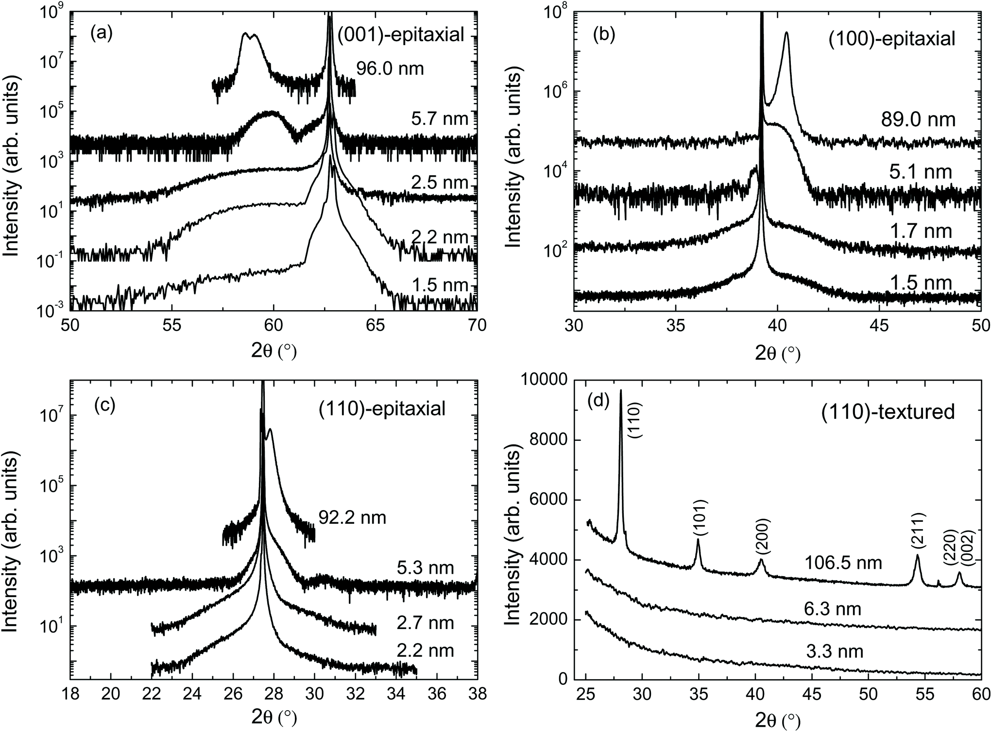 | ||
| Fig. 1 XRD measurements of the (a) (001)-epitaxial, (b) (100)-epitaxial, (c) (110)-epitaxial and (d) (110)-textured films with different thickness. | ||
| Orientation | t (nm) | a(εa) | b(εb) | c(εc) |
|---|---|---|---|---|
| a Estimated from deposition time. | ||||
| (001) | 96.0 | — | — | — |
| (001) | 5.7 | 4.59 (+2.0%) | 4.59 (+2.0%) | 3.11 (−1.6%) |
| (001) | 2.5 | — | — | — |
| (001) | 2.2 | — | — | — |
| (001) | 1.5 | — | — | — |
| (100) | 89.0 | 4.46 (−0.9%) | 4.59 (+2.0%) | 3.13 (−0.9%) |
| (100) | 5.1 | 4.48 (−0.4%) | 4.59 (+2.0%) | 3.10 (−1.9%) |
| (100) | 1.7 | — | — | — |
| (100) | 1.5 | — | — | — |
| (110) | 92.2 | — | — | — |
| (110) | 5.3 | — | — | — |
| (110) | 2.7 | — | — | — |
| (110) | 2.2 | — | — | — |
| (110)-text | 106.5 | 4.49(−0.2%) | 4.49(−0.2%) | 3.13 (−0.9%) |
| (110)-text | 6.3 | — | — | — |
| (110)-text | 3.3 | — | — | — |
| (110)-text | 1.4a | — | — | — |
The panels (a), (b) and (c) of Fig. 1 show the HR-XRD data of the epitaxially grown IrO2 samples. Only Bragg peaks corresponding to the substrate orientation were observed in each sample as expected from their epitaxial growth. The peak position is slightly dependent on the layer thickness indicating modifications of the out of plane lattice parameter resulting from epitaxial strain. The lattice parameters for the (001) and (100)-epitaxial films were calculated from the reciprocal space maps collected on selected 100 nm- and 5 nm-thick samples (see Fig. S4 in the ESI†). The values are summarized in Table 1. As rutile TiO2 substrates with nominal lattice parameters a = b = 4.59 Å and c = 2.96 Å were employed, the IrO2 films present different degrees of tensile/compressive strain depending on substrate orientation. Thus, the t ∼ 5 nm-thick (001)-epitaxial sample presents a large tensile in-plane strain that is not fully compensated by a decrease of the out-of plane c direction, causing a significant modification of the unit cell volume (εa = εb = 2.0%, εc = −1.6% and ΔV/V0 = 2.4%). In contrast, the (110)-textured sample presents almost unstrained a and b lattice parameters (εa = εb = −0.2%) and a small compression along the c direction (εc = −0.9%) resulting in a volume decrease ΔV/V0 = −1.4%. On the other hand, growing the films with (100) orientation barely modifies the total volume (|ΔV/V0| < 0.4%) but results in remarkably dissimilar a and b parameters. It is to be noted here that the a, b and c unit cell axes are not oriented along the octahedral axis in the rutile structure.
Further structural characterization of the films is exemplified in Fig. 2. A flat surface morphology is confirmed for ultrathin films by atomic force microscopy topography. It can be seen that both sample and substrate present similar roughness with maximum Z heights below 0.6 nm and rms ∼0.2 nm, thus showing the continuity of the film. A flat interfacial plane is also observed in the cross-sectional STEM images. Crystal defects are not substantially detected. Representative rocking curves, further showing the good structural quality of the films have been included in the ESI.†
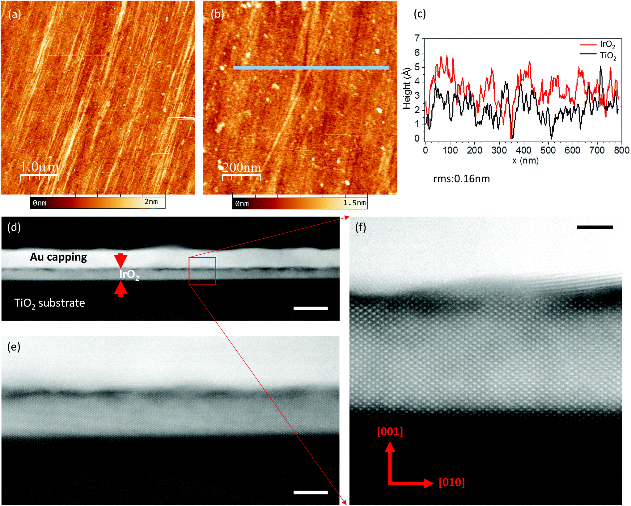 | ||
| Fig. 2 (a) and (b) RT Atomic force microscopy (AFM) image of a 2 nm (001) IrO2 film.(c) Profile along the line shown in (b) compared to the profile measured on a TiO2 substrate. The root mean square roughness is 0.16 nm. (d)–(f) STEM high angle annular dark field images of a ∼5 nm IrO2 thin film on the TiO2 [001] susbtrate. (d) and (e) low magnification images and (f) high resolution image of the framed area in (d) show the epitaxial IrO2/TiO2 interface. Red arrows indicate the zone axis of the TiO2 [001] substrate. Scale bars are 20 nm, 5 nm and 2 nm, respectively. | ||
The (110)-textured polycrystalline film with t ∼ 100 nm displays the typical peaks of rutile-IrO2, with the relative intensity of the (110)-peak clearly enhanced (Fig. 1(d)). For smaller thicknesses, no diffraction peaks can be discerned due to the small amount of material present in the thinnest samples. Even when some loss of crystallinity cannot be ruled out, the well-defined features in the XAS spectra (see Fig. S3 in the ESI†) confirm their crystalline (non-amorphous) character.
The HERFD-XANES spectra were recorded at the Ir L2,3 edges to get a hint on the possible changes in both the electronic structure and SOC. (The branching ratio, i.e. the ratio of the integrated white line intensity recorded at the Ir L2,3 absorption edges, BR = IL3/IL2, is related to the angular part of the spin–orbit interaction 〈L·S〉, see the ESI† for details). Very similar spectral profiles can be observed irrespective of the degree of crystallinity, thickness and strain; therefore, large and mostly constant SOC values are inferred in all the cases, as shown in the representative case displayed in Fig. 3. Nevertheless, a slightly increasing branching ratio is found as the thickness is reduced. Although the differences between 100 nm and 1.5 nm thick samples are in general smaller than 10%, the trend is robust. In contrast, no clear trend can be discerned as the strain is modified by the growth on substrates with different crystalline orientations (See the ESI† for a detailed discussion).
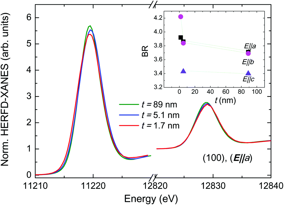 | ||
| Fig. 3 Comparison of the normalized Ir L2,3-edges HERFD-XANES spectra recorded on samples with different thicknesses in (100)-epitaxial samples. The inset plots the evolution of the branching ratio with thickness. | ||
All the thick samples (i.e. t > 3 nm) present the typical metallic behavior of IrO2 characterized by a monotonically slightly increasing electrical resistivity, dρ/dT > 0, over the whole temperature range (Fig. 4). For the thickest samples, t ∼ 90 nm, electrical resistivity in the 30–55 μΩ cm range is obtained at the lowest temperature, T = 10 K, with residual resistivity ratios, RRR = R (300 K)/R(10 K), in the 1.6–2.0 range (detailed table in the ESI†). These values are in good agreement with other previously reported values for epitaxial films.29–31 The low temperature-dependent contribution ρ(T) fits well to a T2-dependence indicating that the electron–electron scattering dominates the temperature dependent part of the electrical resistivity, i.e., a typical Fermi liquid behavior.
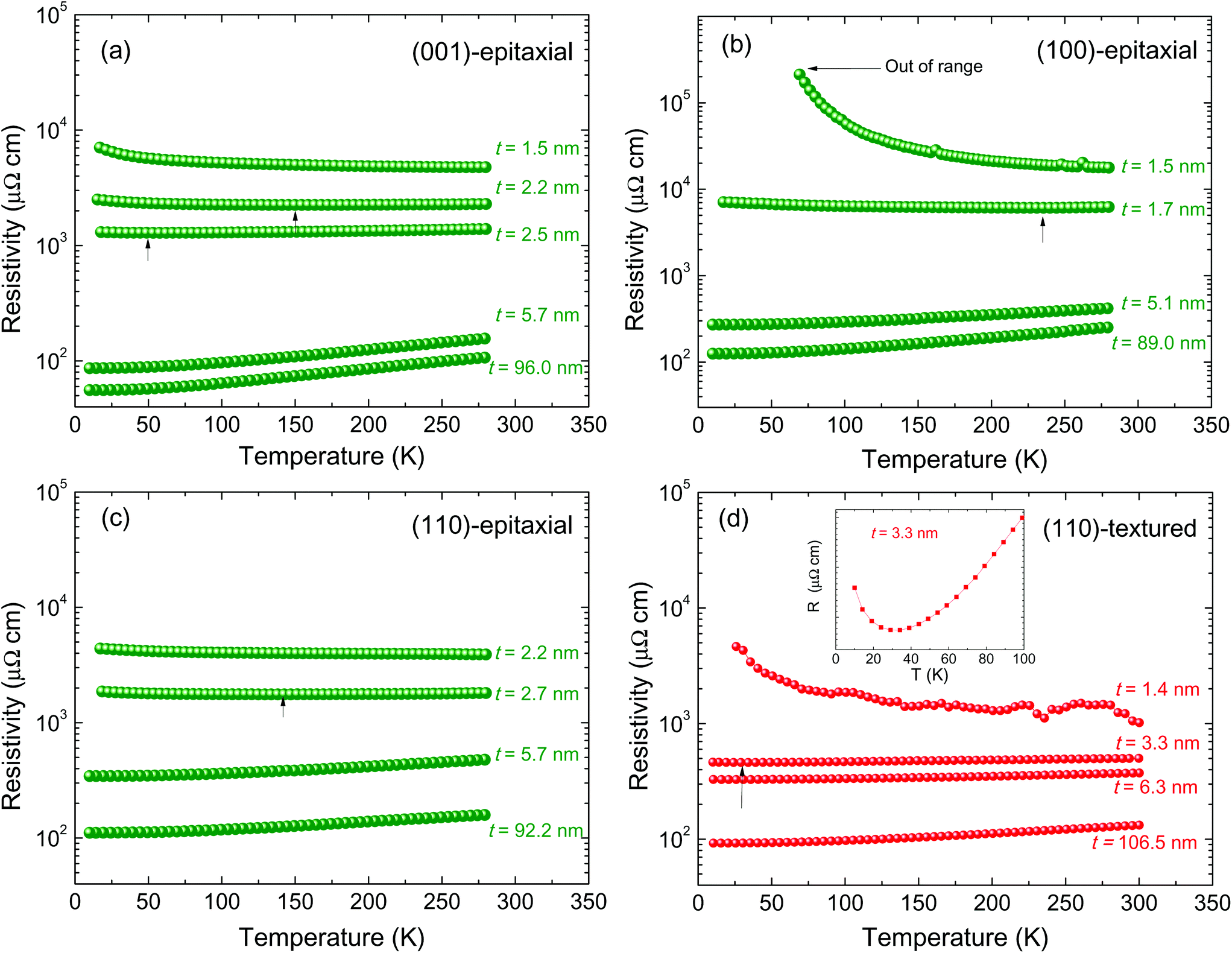 | ||
| Fig. 4 ρ(T) curves for the (a) (001)-epitaxial, (b) (100)-epitaxial, (c) (110)-epitaxial and (d) (110)-textured samples with different thicknesses. Vertical arrows mark the position of upturns. | ||
As t decreases, not only the residual resistivity due to defects, impurities, size effects, and grain boundary scattering increases but also the thermal dependence varies. For the ∼2–3 nm-thick films, a slope change from dρ/dT > 0 at high temperature to dρ/dT < 0 at low temperature is observed at Tmin, marked with arrows in Fig. 4 (zoomed images in the ESI†). This kind of low temperature upturns in resistivity is often observed when a system approaches an MIT from the metallic side.13,32–34 Furthermore, Tmin is located at increasingly higher temperatures as the thickness is reduced. This behavior is related to the progressive localization of the system with thickness reduction, which, in turn, makes the bands closer to the Fermi level progressively depopulated for a given temperature. In this respect, a similar behavior observed in SrIrO3 has been proposed to be related to the semimetallic electronic structure where the hole bands lying just below the Fermi level will be progressively depopulated with decreasing temperature.8 For the thinnest samples (t = 1.5 nm for the (001) and (001) samples and t = 2.2 nm for the (110) sample), dρ/dT < 0 is observed in the whole temperature range. Therefore, it is concluded that the IrO2 crystalline films undergo a thickness-driven MIT within the 1.5–2.5 nm range. Such layer thicknesses correspond to 3–5 unit cells, being quite in agreement with the theoretical predictions.18,20 The comparison between the different panels in Fig. 4 indicates that thickness reduction is more effective in inducing an MIT in the case of (100)-oriented samples and less effective for (001) orientation. Interestingly from the applied point of view, the thinnest polycrystalline (110)-textured film also shows a dρ/dT < 0 behavior over the whole temperature range.
While recent works on IrO2/TiO2 superlattices35 could not find this MIT, it has to be noted that the superlattices of ref. 35 are distinctly different from IrO2 single films, since the former may be affected by interlayer coupling by ultrathin (2 atomic planes) TiO2 spacers. In particular, the superlattices are probably affected by additional hopping channels between the IrO2 layers, as observed in (SrIrO3)/(SrTiO3)m superlattices.36 By studying single IrO2 layers of different thicknesses, the effect of dimensionality on IrO2 is directly addressed.
Fig. 5(a) shows the sheet resistance, Rs, as a function of temperature for representative samples (Rs = Rπ/ln(2), with R being the electrical resistance). It can be seen that Rs continuously increases as the film thickness is reduced. In addition, the change in the electrical behavior occurs when Rs crosses the 25 kΩ value, i.e. the so-called Mott-Ioffe-Regel limit. In very thin films (∼2D), kFl = (h/e2)/Rs ≈ 25 kΩ/Rs, with l being the mean free path and kF the Fermi wave-vector. Rs = 25 kΩ corresponds to the limit where kFl = 1. The above criterion defines a crossover between weak and strong localization.37
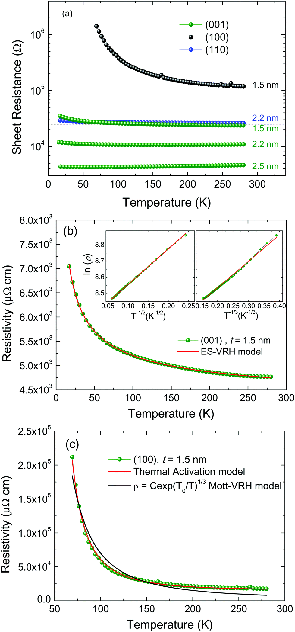 | ||
| Fig. 5 (a) Sheet resistance calculated for the thinnest (001)- and (100)-epitaxial films. (b) ρ(T) curve for the t = 1.5 nm (001)-epitaxial sample fitted to a ES-VRH model. Inset on the left (right) shows the fit to the ES-VRH model with n = 1/2 (disorder-driven localization 2D Mott-VRH model, n = 1/3). (c) ρ(T) curve for the t = 1.5 nm (100)-epitaxial sample fitted to a thermal activation model (red) and a 2D Mott-VRH model (black). | ||
Trying to shed some light on the mechanisms underlying the MIT, the most resistive curves were fitted to several models, see Fig. 5(b) and (c). The resistivity of the (001)-epitaxial film with t = 1.5 nm has a sheet resistance very close to h/e2 at RT and an insulating behavior is found at all temperatures. For this strongly localized regime, a variable range hopping (VRH) type of conduction is expected. Electrons hop between the localized states and the resistivity is given by:38,39
ρ = C![[thin space (1/6-em)]](https://www.rsc.org/images/entities/char_2009.gif) exp(T0/T)n exp(T0/T)n | (1) |
| ρ = Cexp(Eg/2KBT) | (2) |
Therefore, we find that the thickness reduction of IrO2 films yields an MIT. Best fits are obtained in the case of the thinnest samples to either an ES-VRH or an Arrhenius model. Both the hopping (ES-VRH) and thermal activation mechanisms indicate a gap opening that may be associated with an enhanced role of correlations. Nevertheless, several mechanisms could coexist and, for example, an additional contribution of disorder should not be ruled out at this point. In fact, the low temperature region of resistivity curves showing an upturn has been commonly accounted for in terms of weak (Anderson) localization, a disorder-driven effect due to the quantum interference of the conducting charge carriers at defect sites. In the same way, a dissimilar presence of structural defects combined with the ultrathin thickness could also be contributing to the differences in resistivity observed in the work by Kawasaki et al.41 Thus, although the TEM characterization of our samples is in disagreement with the presence of a substantial amount of defects and a major role of disorder, an additional contribution of disorder should not be ruled out. Similarly, the role of SOC and spin fluctuations should be explored. In this regard, it seems unlikely that the little enhancement of the SOC inferred from our data alone may drive the MIT. On the other hand, as a result of the enhanced localization in the thinnest samples (W reduction), the effective SOC increases and the role of the SOC may become more relevant. The presence of the SOC could, for instance, reduce the value of U necessary for the MIT. Further work is required to fully describe the nature of this thickness-driven MIT and the role of the different interactions.
While no MIT has been reported for single IrO2 thin films to date, it may be illustrative at this point to compare with previous works on SrIrO3 thin films of variable thicknesses. Thus, our experimental findings are in agreement with those reported by Groenendijk et al.,8 who point out the major role of correlations.
In contrast to the thickness dependence, no significant modification of ρ(T) can be attributed to a strain-driven effect. As observed in Fig. 6, samples with large differences in their lattice parameters display very similar resistivity curves. For instance, the t ∼ 5 nm-thick (001)-epitaxial sample (with εa = 2.0%, εb = 2.0% and εc = −1.6%) presents a very similar resistivity to that of the (110)-textured sample (with εa = −0.2%, εb = −0.2% and εc = −0.9%) This behavior is noticeably different from that observed in SrIrO3, where a 35 nm-thick film deposited on NdGaO3 (with εa = 2.5% and εc = −2.7%) results in dρ/dT < 0 over the whole temperature range.11,13 Such a different response to the substrate-driven strain could be related to the structural differences of these iridates; while the IrO6 octahedra in IrO2 share corners and edges, in SrIrO3 they are only corner-sharing. This results in an initially broader bandwidth as well as in a more rigid structure in the case of IrO2. Consequently, although a similar substrate-driven strain is achieved in both SrIrO3 and IrO2 cases, it seems not to be enough to significantly reduce W in IrO2.
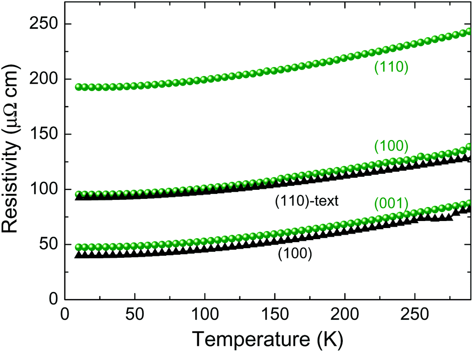 | ||
| Fig. 6 Comparison of the representative ρ(T) curves measured in samples with different substrate-driven strains, t ≈ 5 nm (green circles) and t ≈ 100 nm (black triangles). | ||
It is be noted, however, that a strain-driven effect still could become important in combination with ultrathin films. In this sense, Kawasaki et al.41 report only a slight upturn at low temperatures for ultrathin IrO2 film. We propose that these differences in the transport behaviour can be ascribed to different lattices matching with the substrate and so to different lattice parameters and distortions.
No hint of magnetic order is observed in the M(H) measurements regardless of the thickness, growth orientation or strain (not shown). On the other hand, the temperature-dependent magnetization curves suggest that magnetic order may appear for thin enough films. In particular, all the samples but the most insulating one show a roughly paramagnetic behavior, typically expected for IrO2, as illustrated by the curve recorded on the 1.5 nm-thick (001)-epitaxial film (Fig. 7(a)). However, a weak ferromagnetic-like transition with TC ∼ 125 K is observed in the 1.5 nm-thick (100)-epitaxial film superimposed to the paramagnetic response (Fig. 7(b)). Zero-field-cooled (ZFC) and field-cooled (FC) curves split at a temperature slightly below TC. This fact might indicate that weak ferromagnetism arises from a canted antiferromagnetic order, as occurs in Sr2IrO442 or Sn-doped SrIrO3,15,17 and is also in agreement with the theoretical predictions on IrO2.18,20 It should be noted here that macroscopic magnetic data can hardly unambiguously confirm or discard a change in the magnetic behavior of such thin films. In particular, the maximum values (∼1 × 10⁻⁵ emu cm−2) expected for these films are not only very small but similar to the typical uncertainties associated with the slightly imperfect correction of the background contribution. Therefore, slight differences in the magnetization cannot be undoubtedly associated with the magnetic behavior of the IrO2 layer. Despite that, it can be observed that the magnetic transition appears approximately in the same temperature range at which electrical resistivity shows a drastic increase (see Fig. 4(b)). This would support that it is indeed associated with the IrO2 layer and a related origin for both magnetic and electric transition. In addition, it is to be noted that the magnetic transition is observed only for the (100)-oriented 1.5 nm-thick film, which is far more resistive than the (001)- and (110)-oriented samples. Altogether this suggests a relationship between magnetic and electrical behaviors in such a way that the onset of magnetic ordering would make the sample more resistive. However, the role of magnetic interactions in driving gap formation or gap enhancement has remained a matter of debate in different iridates (see for example43) and further work is needed to clarify this point.
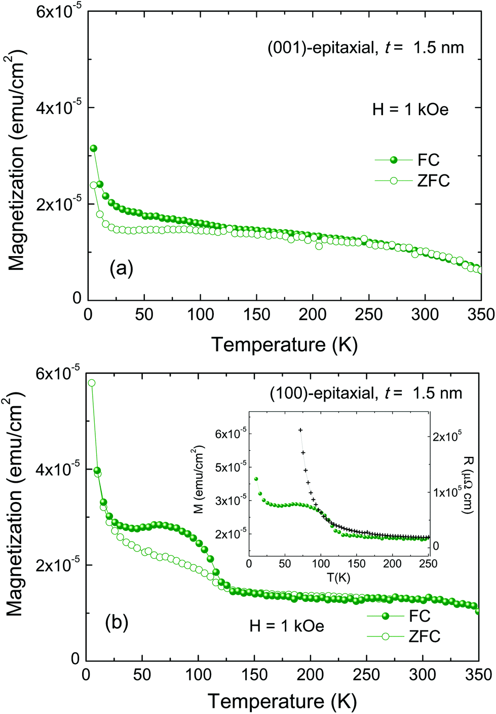 | ||
| Fig. 7 (a) FC/ZFC M(T) curves measured on the t = 1.5 nm (001)-epitaxial IrO2 film. These curves correspond to H in-plane, but no hint of magnetic order is observed with H out-of-plane. (b) FC/ZFC M(T) curves measured with H applied in-plane on the t = 1.5 nm (100)-epitaxial IrO2 film. The inset of panel (b) shows a direct comparison to the thermal dependence of the resistivity. | ||
Contrary to the macroscopic magnetization data, the XMCD data are unambiguously related to the IrO2 layer and allow us to discard any spurious origin. The XMCD spectrum recorded at the Ir L2,3 edges of the t = 1.5 nm (100)-epitaxial sample, i.e. the sample exhibiting the largest electrical resistivity and hints of magnetic ordering in the M(T) curves at low temperatures, is shown in Fig. 8. A small XMCD signal (0.4%) can be inferred at the L3 edge. The presence of an XMCD signal at the Ir L2 edge is ambiguous. If any, its size is much smaller than that at the L3 edge. The position, shape and sign of the small signal observed agree well with previous XMCD measurements carried out in other Ir4+-based compounds, such as in Sr2IrO4,43 Sr2TiIrO644 or BaIrO3.45 In addition, the XMCD spectrum of powdered IrO2 presents a much smaller intensity (Fig. 8(b)). These comparisons point out that the small XMCD signal may indeed be associated with the magnetic ordering of the Ir4+ cations or, at least, with an enhanced paramagnetic signal of this film. Therefore, although further work is needed to verify the presence of magnetic order, these results are the first experimental evidence supporting that magnetic ordering can be achieved in IrO2 through structural modifications (thickness reduction) as proposed by theoretical predictions.18,20 In addition, the fact that the magnetic transition appears in the same temperature range where the electrical resistivity drastically increases might indicate an important role of magnetic order in the opening of the electronic gap, i.e. an unconventional Mott–Slater-type insulator. Finally, the sum-rules analysis46,47 indicates that the net orbital magnetic moment is ml ∼ 0.003μB/Ir and the spin magnetic moment ms ∼ 0.007μB/Ir (0.005μB/Ir) if Tz = 0 (14〈Tz〉/〈4Sz〉 = 0.6445) is assumed. The orbital to spin moment ratio is a factor ∼4 smaller than the ml/ms = 2 proposed for a Jeff = 1/2 state, indicating a deviation from the pure Jeff = 1/2 state.
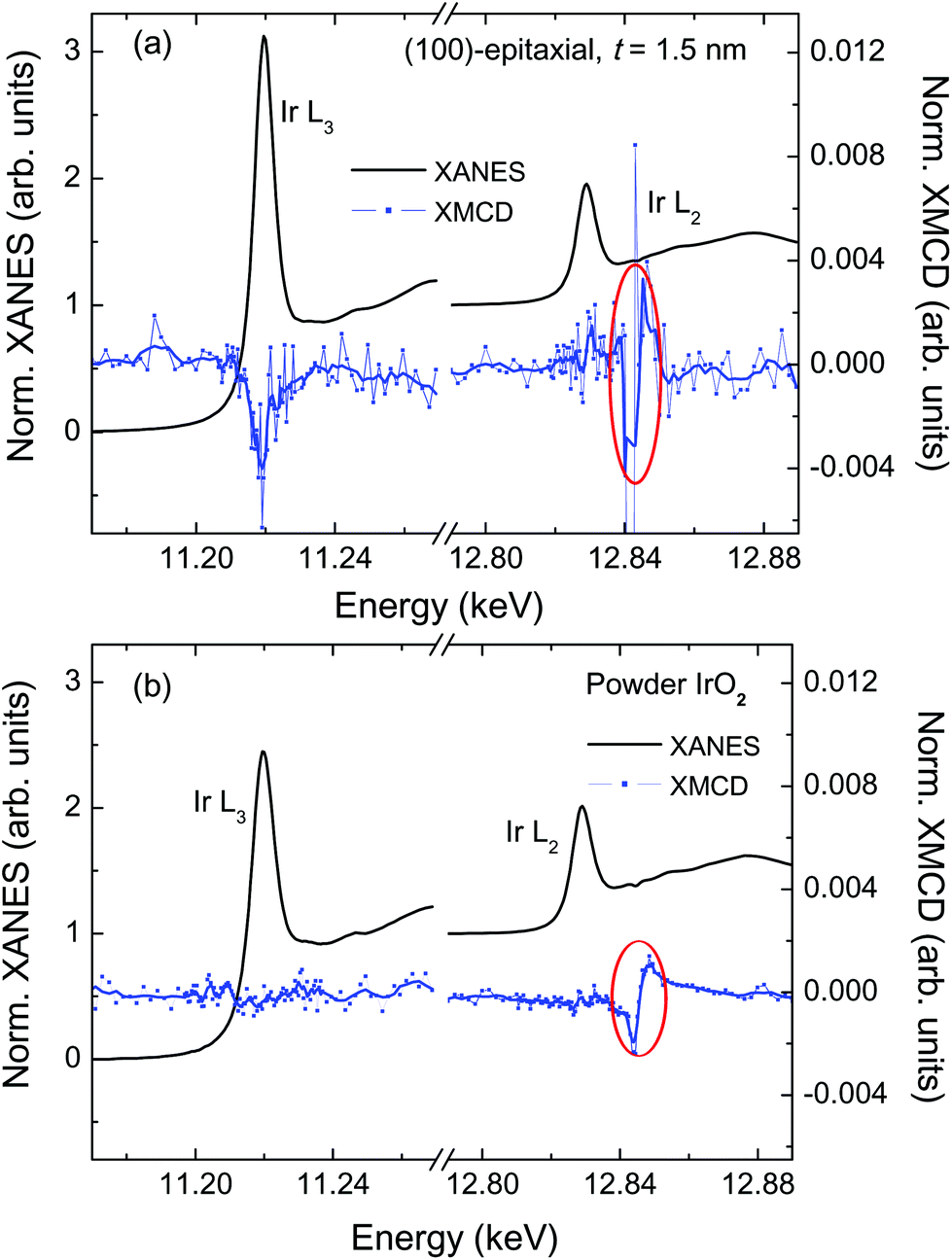 | ||
| Fig. 8 (a) Normalized XANES and XMCD spectra recorded in the fluorescence mode at the Ir L2,3 edges at T = 10 K and H = ±50 kOe on the t = 1.5 nm (100)-epitaxial sample. (b) Normalized XANES and XMCD spectra measured in the transmission mode at the Ir L2,3 edges at T = 10 K and H = ±35 kOe on commercial powdered IrO2. The lower intensity of the XAS white line is due to a 4% of metal Ir phase. Solid blue lines indicate a smoothing of the experimental data (in solid symbols). Red circles indicate a spurious artifact due to a monochromator glitch at that energy. | ||
4. Conclusions
The relationships between the structure of IrO2 thin films and their electrical and magnetic properties have been studied. The SOC in IrO2 thin films is very large and robust, being mostly independent of the structural details. A small (∼1–10%) but reproducible increment of the SOC is observed for the thinnest samples. Regarding the electrical characterization, upon reducing the IrO2 film thickness, the response evolves from a metallic ground state to a strongly localized behavior as the RT sheet resistance approaches h/e2 ≈ 25 kΩ for ∼1.5 nm. At around 2–3 nm-thickness, the films show upturns in resistivity at low temperatures. Upon further reducing the thickness of the deposited layer to ∼1.5 nm, a small band gap is opened suggesting an enhanced role of electron correlations (U/W). As for the magnetic properties, the temperature magnetization curves suggest the presence of magnetic ordering (canted AFM) at low temperatures in the thinnest samples. The XMCD measurements also support this hypothesis. In addition, it is found that the magnetic transition occurs at the same temperature at which the resistivity shows a strong increase, pointing to an interplay between magnetism and electrical behavior. Overall, our results are consistent with a combined effect of electron correlations and magnetic order as the mechanisms responsible for the thickness-dependent MIT found in IrO2 thin films (Mott–Slater-like insulator). This research highlights ultrathin IrO2 films as a novel platform for tuning the electrical and magnetic response of this material. Finally, it is worth noticing the potential relevance of combining the tunability in resistivity here shown with other interesting features of IrO2, namely, its large spin Hall effect (SHE),48 its nonsymmorphic crystalline symmetry that allows the switching of the charge carrier type29 and its easy growth relative to other iridates.Conflicts of interest
There are no conflicts to declare.Acknowledgements
This work was partially supported by the Spanish MINECO projects MAT2014-54425-R (MINECO/FEDER, UE), MAT2017-82970-C2-R (AEI/FEDER, UE), MAT2017-83468-R (AEI/FEDER, UE), MAT2017-87134-C02-01-R (AEI/FEDER, UE) and MAT2017-87134-C02-02-R (AEI/FEDER, UE), the Spanish MICINN project PID2020-115159GB-I00 / AEI / 10.13039/501100011033 and by the Aragon Regional Government (Projects No. E12-20R and E28-20R). E. A-E acknowledges the Spanish MINECO and the European Social Fund for an FPI (Formación de Personal Investigador, 2015) grant. R. B. acknowledges funding support from the European Union's Horizon 2020 research and innovation program under the Marie Skłodowska-Curie grant agreement no. 665919. This research used resources of the APS, a U.S. Department of Energy (DOE) Office of Science User Facility operated for the DOE Office of Science by Argonne National Laboratory under Contract No. DE-AC02-06CH11357. We acknowledge Diamond Light Source for time on I20-Scanning under Proposal SP-17266. The research leading to this result has been supported by the project CALIPSOplus under the Grant Agreement 730872 from the EU Framework Programme for Research and Innovation Horizon 2020. The authors acknowledge funding from the project Quantox of QuantERA ERA-NET Cofund of Quantum Technologies (Grant Agreement No. 731473) implemented within the European Union's Horizon 2020 Programme. The authors would like to acknowledge the use of Servicio General de Apoyo a la Investigación-SAI, Universidad de Zaragoza. The authors would like to acknowledge the use of the diffractometers at the Instituto de Nanociencia de Aragón and C. Munuera for AFM images.References
- D. Haskel, G. Fabbris, M. Zhernenkov, P. P. Kong, C. Q. Jin, G. Cao and M. van Veenendaal, Phys. Rev. Lett., 2012, 109, 027204 CrossRef CAS PubMed.
- G. Cao and P. Schlottmann, Rep. Prog. Phys., 2018, 81, 042502 CrossRef PubMed.
- J. G. Rau, E. K.-H. Lee and H.-Y. Kee, Annu. Rev. Condens. Matter Phys., 2016, 7, 195–221 CrossRef CAS.
- W. Witczak-Krempa, G. Chen, Y. B. Kim and L. Balents, Annu. Rev. Condens. Matter Phys., 2014, 5, 57–82 CrossRef CAS.
- C. R. Serrao, J. Liu, J. T. Heron, G. Singh-Bhalla, A. Yadav, S. J. Suresha, R. J. Paull, D. Yi, J.-H. Chu, M. Trassin, A. Vishwanath, E. Arenholz, C. Frontera, J. Železný, T. Jungwirth, X. Marti and R. Ramesh, Phys. Rev. B: Condens. Matter Mater. Phys., 2013, 87, 085121 CrossRef.
- J. Nichols, J. Terzic, E. G. Bittle, O. B. Korneta, L. E. D. Long, J. W. Brill, G. Cao and S. A. Seo, Appl. Phys. Lett., 2013, 102, 141908 CrossRef.
- A. Lupascu, J. P. Clancy, H. Gretarsson, Z. Nie, J. Nichols, J. Terzic, G. Cao, S. S. A. Seo, Z. Islam, M. H. Upton, J. Kim, D. Casa, T. Gog, A. H. Said, V. M. Katukuri, H. Stoll, L. Hozoi, J. van den Brink and Y.-J. Kim, Phys. Rev. Lett., 2014, 112, 147201 CrossRef CAS PubMed.
- D. J. Groenendijk, C. Autieri, J. Girovsky, M. C. Martinez-Velarte, N. Manca, G. Mattoni, A. M. R. V. L. Monteiro, N. Gauquelin, J. Verbeeck, A. F. Otte, M. Gabay, S. Picozzi and A. D. Caviglia, Phys. Rev. Lett., 2017, 119, 256403 CrossRef CAS PubMed.
- J. Matsuno, K. Ihara, S. Yamamura, H. Wadati, K. Ishii, V. V. Shankar, H.-Y. Kee and H. Takagi, Phys. Rev. Lett., 2015, 114, 247209 CrossRef CAS PubMed.
- F.-X. Wu, J. Zhou, L. Y. Zhang, Y. B. Chen, S.-T. Zhang, Z.-B. Gu, S.-H. Yao and Y.-F. Chen, J. Phys.: Condens. Matter, 2013, 5, 125604 CrossRef PubMed.
- J. H. Gruenewald, J. Nichols, J. Terzic, G. Cao, J. W. Brill and S. S. Seo, J. Mater. Res., 2014, 29, 2491–2496 CrossRef CAS.
- Y. F. Nie, P. D. C. King, C. H. Kim, M. Uchida, H. I. Wei, B. D. Faeth, J. P. Ruf, J. P. C. Ruff, L. Xie and X. Pan, Phys. Rev. Lett., 2015, 114, 016401 CrossRef CAS PubMed.
- A. Biswas, K.-S. Kim and Y. H. Jeong, J. Appl. Phys., 2014, 116, 213704 CrossRef.
- J. Liu, J.-H. Chu, C. R. Serrao, D. Yi, J. Koralek, C. Nelson, C. Frontera, D. Kriegner, L. Horak, E. Arenholz, J. Orenstein, A. Vishwanath, X. Marti and R. Ramesh, 2013, arXiv:1305.1732v1 [cond-mat.str-el].
- Q. Cui, J.-G. Cheng, W. Fan, A. E. Taylor, S. Calder, M. A. McGuire, J.-Q. Yan, D. Meyers, X. Li, Y. Q. Cai, Y. Y. Jiao, Y. Choi, D. Haskel, H. Gotou, Y. Uwatoko, J. Chakhalian, A. D. Christianson, S. Yunoki, J. B. Goodenough and J.-S. Zhou, Phys. Rev. Lett., 2016, 117, 176603 CrossRef CAS PubMed.
- C. Lu, A. Quindeau, H. Deniz, D. Preziosi, D. Hesse and M. Alexe, Appl. Phys. Lett., 2014, 105, 082407 CrossRef.
- J. Cheng, J. Zhou, J. B. Goodenough, K. Matsubayashi and Y. Uwatoko, JPS Conf. Proc., 2014, 3, 013014 Search PubMed.
- S. K. Panda, S. Bhowal, A. Delin, O. Eriksson and I. Dasgupta, Phys. Rev. B: Condens. Matter Mater. Phys., 2014, 89, 155102 CrossRef.
- J. M. Kahk, C. G. Poll, F. E. Oropeza, J. M. Ablett, D. CÃolin, J. Rueff, S. Agrestini, Y. Utsumi, K. D. Tsuei and Y. F. Liao, Phys. Rev. Lett., 2014, 112, 117601 CrossRef CAS PubMed.
- X. Ming, K. Yamauchi, T. Oguchi and S. Picozzi, 2017, arXiv:1702.04408 [cond-mat.str-el], 89.
- M. Varela, W. Grogger, D. Arias, Z. Sefrioui, C. León, C. Ballesteros, K. M. Krishnan and J. Santamaría, Phys. Rev. Lett., 2001, 86, 5156–5159 CrossRef CAS PubMed.
- G. Sanchez-Santolino, J. Tornos, D. Hernandez-Martin, J. I. Beltran, C. Munuera, M. Cabero, A. Perez-Munoz, J. Ricote, F. Mompean, M. Garcia-Hernandez, Z. Sefrioui, C. Leon, S. J. Pennycook, M. C. Munoz, M. Varela and J. Santamaria, Nat. Nanotechnol., 2017, 12, 655–662 CrossRef CAS PubMed.
- M. Cabero, K. Nagy, F. Gallego, A. Sander, M. Rio, F. A. Cuellar, J. Tornos, D. Hernandez-Martin, N. M. Nemes, F. Mompean, M. Garcia-Hernandez, A. Rivera-Calzada, Z. Sefrioui, N. Reyren, T. Feher, M. Varela, C. Leon and J. Santamaria, APL Mater., 2017, 5, 096104 CrossRef.
- L. J. van der Pauw, Philips Res. Rep., 1958, 13, 1 Search PubMed.
- S. Diaz-Moreno, M. Amboage, M. Basham, R. Boada, N. E. Bricknell, G. Cibin, T. M. Cobb, J. Filik, A. Freeman, K. G. D. Gianolio, S. Hayama, K. Ignatyev, L. Keenan, I. Mikulska, J. F. W. Mosselmans, J. J. Mudd and S. A. Parry, J. Synchrotron Radiat., 2018, 25, 998 CrossRef PubMed.
- S. Diaz-Moreno, S. Hayama, M. Amboage, A. Freeman, J. Sutter and G. Duller, J. Phys.: Conf. Ser., 2009, 190, 012038 CrossRef.
- S. Hayama, G. Duller, J. P. Sutter, M. Amboage, R. Boada, A. Freeman, L. Keenan, B. Nutter, L. Cahill, P. Leicester, B. Kemp, N. Rubies and S. Diaz-Moreno, J. Synchrotron Radiat., 2018, 25, 1556 CrossRef CAS PubMed.
- E. Arias-Egido, M. A. Laguna-Marco, C. Piquer, R. Boada and S. Diaz-Moreno, Adv. Funct. Mater., 2019, 29, 1806754 CrossRef.
- M. Uchida, W. Sano, K. S. Takahashi, T. Koretsune, Y. Kozuka, R. Arita, Y. Tokura and M. Kawasaki, Phys. Rev. B, 2015, 91, 241119 CrossRef.
- A. Bose, J. N. Nelson, X. S. Zhang, P. Jadaun, R. Jain, D. G. Schlom, D. C. Ralph, D. A. Muller, K. M. Shen and R. A. Buhrman, ACS Appl. Mater. Interfaces, 2020, 12, 55411–55416 CrossRef CAS PubMed.
- W. J. Kim, S. Y. Kim, C. H. Kim, C. H. Sohn, O. B. Korneta, S. C. Chae and T. W. Noh, Phys. Rev. B, 2016, 93, 045104 CrossRef.
- L. Wang, L. Chang, X. Yin, A. Rusydi, L. You, Y. Zhou, L. Fang and J. Wang, J. Phys.: Condens. Matter, 2017, 29, 025002 CrossRef PubMed.
- X. Shen, X. Qiu, D. Su, S. Zhou, A. Li and d D. Wu, J. Appl. Phys., 2015, 117, 015307 CrossRef.
- R. Scherwitzl, S. Gariglio, M. Gabay, P. Zubko and M. G. M. Triscone, Phys. Rev. Lett., 2011, 106, 246403 CrossRef CAS PubMed.
- J. K. Kawasaki, D. Baek, H. Paik, H. P. Nair, L. F. Kourkoutis, D. G. Schlom and K. M. Shen, Phys. Rev. Mater., 2018, 2, 054206 CrossRef CAS.
- L. Hao, D. Meyers, C. Frederick, G. Fabbris, J. Yang, N. Traynor, L. Horak, D. Kriegner, Y. Choi, J.-W. Kim, D. Haskel, P. J. Ryan, M. P. M. Dean and J. Liu, Phys. Rev. Lett., 2017, 119, 027204 CrossRef PubMed.
- D. C. Licciardello and D. J. Thouless, Phys. Rev. Lett., 1975, 35, 1475–1478 CrossRef CAS.
- N. F. Mott, Metal Insulator Transitions, Taylor and Francis, London, 1990 Search PubMed.
- N. F. Mott and E. A. Davies, Electron Processes in Non-Crystalline Materials, Clarendon, Oxford, 1979 Search PubMed.
- A. L. Efros and B. I. Shklovskii, J. Phys. C: Solid State Phys., 1975, 8, L49–L51 CrossRef CAS.
- J. K. Kawasaki, C. H. Kim, J. N. Nelson, S. Crisp, C. J. Zollner, E. Biegenwald, J. T. Heron, C. J. Fennie, D. G. Schlom and K. M. Shen, Phys. Rev. Lett., 2018, 121, 176802 CrossRef CAS PubMed.
- F. Ye, S. Chi, B. C. Chakoumakos, J. A. Fernandez-Baca, T. Qi and G. Cao, Phys. Rev. B: Condens. Matter Mater. Phys., 2013, 87, 140406R CrossRef.
- D. Haskel, G. Fabbris, M. Zhernenkov, P. Kong, C. Jin, G. Cao and M. van Veenendaal, Phys. Rev. Lett., 2012, 109, 027204 CrossRef CAS PubMed.
- M. A. Laguna-Marco, P. Kayser, J. Alonso, M. Martinez-Lope, M. van Veenendaal, Y. Choi and D. Haskel, Phys. Rev. B., 2015, 91, 214433 CrossRef.
- M. A. Laguna-Marco, D. Haskel, N. Souza-Neto, J. C. Lang, V. V. Krishnamurthy, S. Chikara, G. Cao and M. van Veenendaal, Phys. Rev. Lett., 2010, 105, 216407 CrossRef CAS PubMed.
- B. T. Thole, P. Carra, F. Sette and G. van der Laan, Phys. Rev. Lett., 1992, 68, 1943 CrossRef CAS PubMed.
- P. Carra, B. T. Thole, M. Altarelli and X. Wang, Phys. Rev. Lett., 1993, 70, 694 CrossRef CAS PubMed.
- K. Fujiwara, Y. Fukuma, J. Matsuno, H. Idzuchi, Y. Niimi, Y. Otani and H. Takagi, Nat. Commun., 2013, 4, 2893 CrossRef PubMed.
Footnotes |
| † Electronic supplementary information (ESI) available: Structural information of the films and their XANES characterization. See DOI: 10.1039/d1nr04207f |
| ‡ Samples with t ∼ 5 nm were also grown by high pressure sputtering and used to confirm that the resistivity behaviour does not depend on the deposition method but they are not shown here. |
| This journal is © The Royal Society of Chemistry 2021 |