
 Open Access Article
 This Open Access Article is licensed under a
 Creative Commons Attribution 3.0 Unported Licence
Fast response photogating in monolayer MoS2 phototransistors†
Daniel
Vaquero
a,
Vito
Clericò
 a,
Juan
Salvador-Sánchez
a,
Elena
Díaz
b,
Francisco
Domínguez-Adame
b,
Leonor
Chico
bc,
Yahya M.
Meziani
a,
Enrique
Diez
a and
Jorge
Quereda
*a
a,
Juan
Salvador-Sánchez
a,
Elena
Díaz
b,
Francisco
Domínguez-Adame
b,
Leonor
Chico
bc,
Yahya M.
Meziani
a,
Enrique
Diez
a and
Jorge
Quereda
*a
aNanotechnology Group, USAL–Nanolab, Universidad de Salamanca, E-37008 Salamanca, Spain. E-mail: J.Quereda@usal.es
bGISC, Departamento de Física de Materiales, Universidad Complutense, E-28040 Madrid, Spain
cInstituto de Ciencia de Materiales de Madrid, CSIC, E-28049 Madrid, Spain
First published on 7th September 2021
Abstract
Two-dimensional transition metal dichalcogenide (TMD) phototransistors have been the object of intensive research during the last years due to their potential for photodetection. Photoresponse in these devices is typically caused by a combination of two physical mechanisms: the photoconductive effect (PCE) and photogating effect (PGE). In earlier literature for monolayer (1L) MoS2 phototransistors, PGE is generally attributed to charge trapping by polar molecules adsorbed to the semiconductor channel, giving rise to a very slow photoresponse. Thus, the photoresponse of 1L-MoS2 phototransistors at high-frequency light modulation is assigned to PCE alone. Here we investigate the photoresponse of a fully h-BN encapsulated monolayer (1L) MoS2 phototransistor. In contrast with previous understanding, we identify a rapidly-responding PGE mechanism that becomes the dominant contribution to photoresponse under high-frequency light modulation. Using a Hornbeck–Haynes model for the photocarrier dynamics, we fit the illumination power dependence of this PGE and estimate the energy level of the involved traps. The resulting energies are compatible with shallow traps in MoS2 caused by the presence of sulfur vacancies.
A Introduction
Two-dimensional (2D) transition metal dichalcogenides (TMDs) are very attractive for the development of phototransistors and other optoelectronic devices at the nanoscale1–5 due to their optical bandgap spanning the visible spectrum, large photoresponse, and high carrier mobility. In 2D TMD phototransistors, photoresponse typically stems from two main mechanisms:6–12 The photoconductive effect (PCE), where light-induced formation of electron–hole pairs leads to an increased charge carrier density and electrical conductivity; and the photogating effect (PGE),9 where the light-induced filling or depletion of localized states causes a shift of the Fermi energy. When the characteristic relaxation times for these localized states are very long, the light-induced Fermi energy shift persists for a long time after exposure to light. In this case, the effect is commonly referred to as photodoping.13,14The occurrence of PGE in 2D-TMD phototransistors is usually associated with the presence of polar molecules adsorbed onto the monolayer surface,6 resulting in a very slow, atmosphere-dependent photoresponse. Thus, the general understanding is that PGEs can be ruled out simply by modulating the intensity of the optical excitation at relatively fast frequencies (∼10 Hz). The high-frequency response of the device is therefore generally attributed to the PCE.
Here, we investigate the photoresponse of a high-quality h-BN encapsulated monolayer MoS2 phototransistor. In stark contrast with previous understanding, the dependence of the observed photoresponse on the gate voltage and illumination power indicates that PGE is the dominant contribution to photoresponse, even for light-modulation frequencies of up to 1 kHz, much faster than the response time of PGEs described in earlier literature.6 Further, the observed fast-responding PGE remains present even when measuring at cryogenic conditions, where the characteristic times for charge trapping processes involving adsorbed polar molecules should be very long. This suggests the presence of an additional contribution to PGE, not related to adsorption of environmental species but instead caused by impurities in the MoS2 crystal lattice.
The contribution to photoresponse coming from the PGE only fades away when the semiconductor channel is in its off state, i.e., for gate voltages Vg well below the threshold voltage Vth. In this regime, the remaining photoresponse becomes linear with the illumination power, as expected for PCE.
We analyze the dynamics of photoexcited carriers using a Hornbeck–Haynes model6,15 that accounts for PGEs caused by charge trapping at shallow impurities in the MoS2 monolayer (not considered in previous works6). The model allows us to fit with great accuracy the experimentally observed power dependence of photocurrent and extract values for the density of localized states and the characteristic times for filling and depletion of charge traps. Finally, by considering the detailed balance principle, we estimate that the localized states involved in photogating lay at an energy ∼8.4 meV above the valence-band edge. This estimated energy is compatible with shallow trap-states associated with sulfur vacancies, generally present in 2D-MoS2.16–18 Thus, our results suggest that the dominant mechanism for high-frequency photoresponse in monolayer MoS2 phototransistors is a sulfur vacancy-mediated PGE, and not PCE as generally assumed in earlier literature.
B Results and discussion
B.1 Photoconductive and photogating effects
The inset in Fig. 1a schematically shows the 1L-MoS2 transistor geometry: The semiconductor channel is encapsulated between multilayer hexagonal boron nitride (h-BN) flakes in order to better preserve its intrinsic properties19 and Ti/Au electrodes are fabricated on top following an edge-contact geometry (further described in the Methods section). The device is fabricated on a 300 nm SiO2/Si substrate and the bottom Si layer is used as back gate. All the measurements reported in the main text are performed in vacuum and at T = 5 K unless otherwise specified. Similar measurements at room temperature can be found in the ESI, section S1.†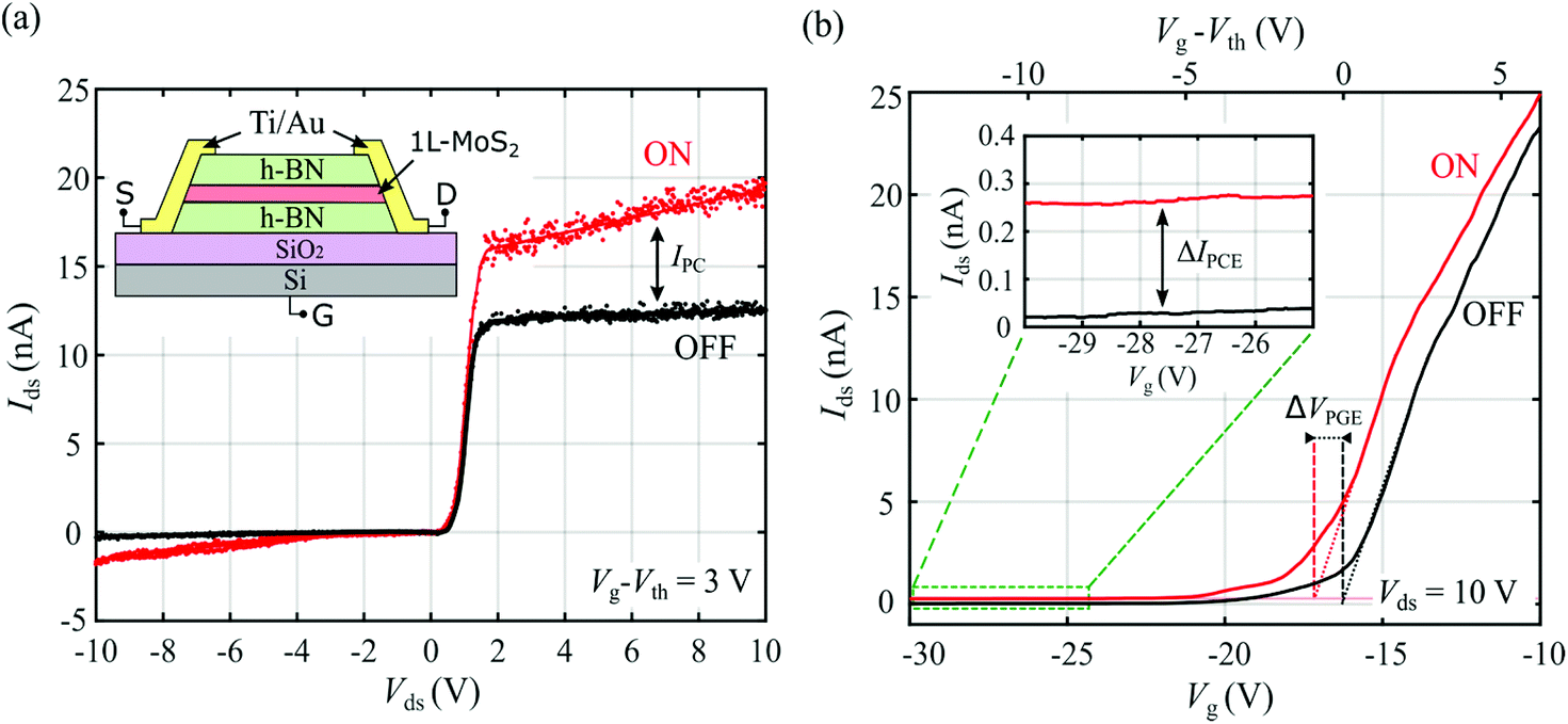 | ||
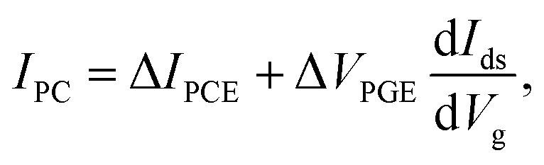
| Fig. 1 Electrical and optoelectronic response of the monolayer MoS2 phototransistor. (a) Two-terminal I–V characteristic of the monolayer MoS2 phototransistor in the dark and under uniform illumination with power density PD = 1 mW mm−2 and photon energy hν = 1.92 eV. Upon illumination the drain–source current, Ids increases by IPC. Inset: Schematic drawing of the device. (b) Gate transfer curves of the device, showing a threshold gate voltage Vth = −11 V. The inset shows a zoom-in of the region indicated by the dashed green rectangle. The contributions to photoresponse by ΔIPCE and ΔVPGE (see eqn (1)) are indicated in the plot. | ||
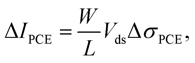
Fig. 1a shows two-terminal I–V curves of the monolayer MoS2 phototransistor, measured both in the dark and while exposing the entire area of the device to uniform illumination with power density PD = 1 mW mm−2 and photon energy hν = 1.92 eV (on resonance with the XA exciton transition of 1L-MoS2). The I–V curves present a back-to-back diode-like behaviour due to the presence of Schottky barriers at the contacts.20,21 The different saturation currents for positive and negative voltages are caused by an asymmetry in the Schottky barrier heights. Upon illumination, the drain–source current IDS increases by IPC due to PCE and PGE. The light-induced increase of current, IPC, can be written as
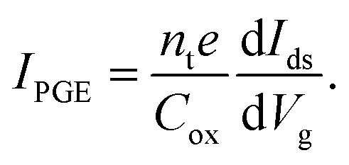
 | (1) |
Fig. 1b shows gate transfer characteristics of the device acquired in the dark and under illumination. In the following, the drain–source voltage is kept at Vds = 10 V for consistency. However, the results presented below for the dependence of IPC on the gate voltage, illumination power and light modulation frequency do not change significantly for lower Vsd.
At low temperature, the transfer curves are almost hysteresis-free, showing a clear n-type behaviour, and the semiconductor channel conductivity increases as the back-gate voltage Vg becomes larger than the threshold voltage Vth. The two contributions to IPC from eqn (1) can be clearly distinguished in Fig. 1b. There, the effect of PGE is observed as a horizontal shift of the transfer curve upon illumination, by the amount ΔVPGE, while PCE results in a smaller but measurable vertical shift by ΔIPCE (see inset in the figure).
The increase in photocurrent caused by the PCE is given by
 | (2) |
| ΔσPCE = q(μnnph + μppph) | (3) |
Here, μn and μp are the electron and hole mobilities respectively, and nph and pph are the densities of optically generated excess charge carriers.
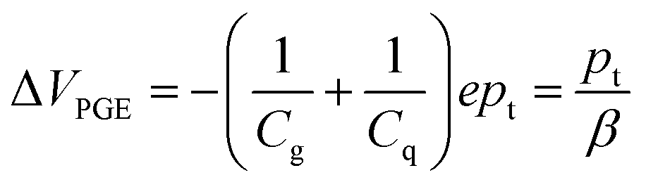
As discussed above, PGE appears when optically excited carriers can fall into trap states. While these trapped carriers do not directly contribute to transport, their presence can result in a partial screening of the gate voltage Vg, modifying the effective threshold voltage Vth of the device, and consequently, the measured current. Assuming that in equilibrium there is a finite density nt of trapped carriers, we can use a parallel-plate capacitor model to estimate the shift ΔVPGE:
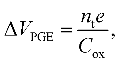 | (4) |
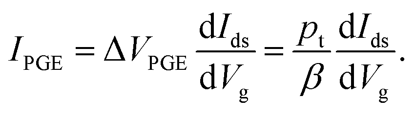
 | (5) |
Thus, IPGE is proportional to the transverse conductance dIds/dVg, which enables us to distinguish it from IPCE, as discussed below.
B.2 Frequency dependence of IPC
We now consider the effect of the light-modulation frequency in the 1L-MoS2 photoresponse. At this point it is useful to compare our results with a previous characterization of photoresponse in a monolayer MoS2 phototransistor, reported by Furchi et al.6 There, while measuring at room temperature, they observed a slow-responding PGE, which they attributed to charge-trapping by few layers of surface-bound water molecules underneath the MoS2 sheet. By using a mechanical chopper to modulate the optical excitation and registering the signal with a lock-in amplifier, they observed that the photocurrent IPC largely decreased for light-modulation frequencies above ∼1 Hz, as the trapping process was too slow to respond to the excitation. Thus they interpreted the remaining high-frequency signal as originated by PCE.For comparison, we now also make use of a lock-in amplifier to measure the dependence of IPC on the light modulation frequency for our device, as shown in Fig. 2a. Similarly to Furchi et al. we also observe a reduction of the signal at higher frequencies. For our measurements at T = 5 K, we find that IPC decreases by roughly a factor 3, while at room temperature we observe a much larger reduction (see ESI section S1†). This weaker reduction at cryogenic temperatures is compatible with the slow-responding PGE caused by adsorbed polar molecules, since the effect of these dipoles should largely decrease at cryogenic temperatures. Interestingly, we find that the frequency dependence of the signal can be modified with the gate voltage, with IPC decaying much more slowly with the modulation frequency for larger gate voltages.
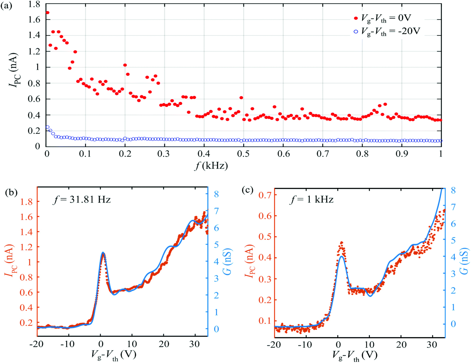 | ||
| Fig. 2 Frequency-dependent photoresponse. (a) IPC as a function of the light-modulation frequency. Measurements are shown for Vg − Vth = −20 V (blue, empty circles; corresponding to the PCE-dominated regime) and for Vg − Vth = 0 V (red, filled circles; PGE-dominated regime). (b) Transconductance (blue line, right axis) and gate-dependent photocurrent (orange dots, left axis) measured at Vds = 10 V for illumination on resonance with the X1sA exciton transition and a light-modulation frequency f = 31.81 Hz. (c) Same as (b) with f = 1 kHz. | ||
Let us now investigate the origin of the remaining signal for high-frequency modulation. As mentioned above, this fast-response contribution to the photocurrent is usually attributed to PCE in earlier literature. However, as we argue below, we find that the behaviour of this fast-response photocurrent can be better described by considering an additional contribution to PGE.
A characteristic signature of PGE is that the resulting photocurrent IPC is proportional to the transconductance G = dIds/dVg of the semiconductor channel (see eqn (5)). This allows us to clearly distinguish it from PCE, which should not have a strong dependence on Vg for low carrier densities. As shown in Fig. 2b, we find that for our 1L-MoS2 device the Vg-dependence of IPC is very strongly correlated to the transconductance G (obtained as the numerical derivative of the I–V transfer characteristic). Importantly, this remains true even when the light is modulated at frequencies as high as 1 kHz (Fig. 2c). This trend indicates that the photoresponse is mainly dominated by PGE even at high frequency, in stark contrast with earlier understanding.6 As discussed below, we attribute this fast-response PGE to charge trapping at sulfur vacancies, present in the 1L-MoS2 crystal.
At gate voltages well below Vth the device shows a smaller, but measurable photocurrent. In this regime the transconductance G is zero and, consequently, the PGE contribution to IPC fades away. We conclude that the small remaining photocurrent for Vg ≪ Vth must be caused by PCE.
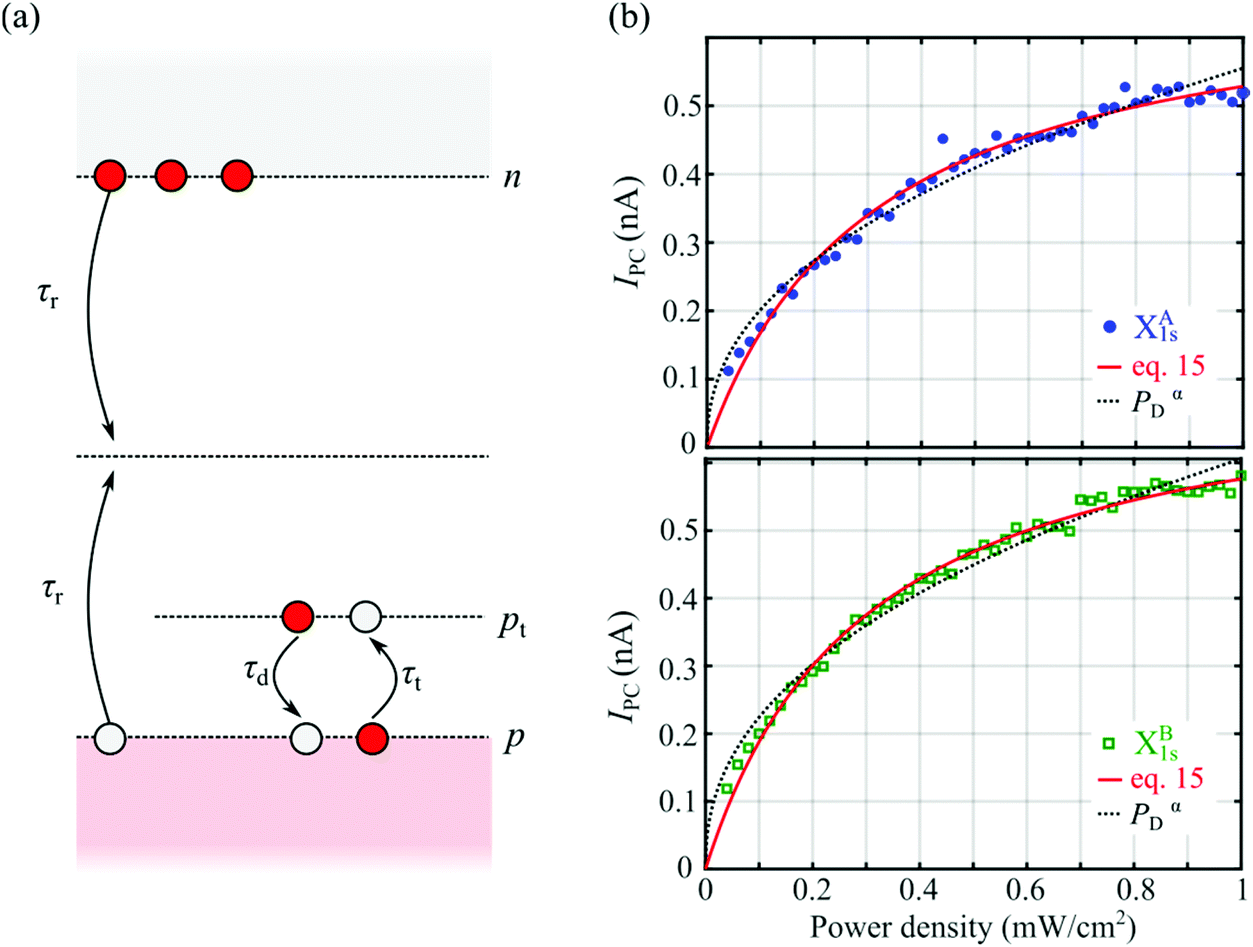
B.3 Power density dependence of IPC
To further confirm our interpretation of the photoresponse for the two gate voltage regimes (Vg ≫ Vth and Vg ≪ Vth) we now study the dependence of IPC on the illumination power density. Fig. 3a shows IPC as a function of the illumination power for Vg − Vth = −20 V at two different photon energies, corresponding to the X1sA (1.92 eV) and X1sB (2.07 eV) excitonic transitions of 1L-MoS2 (see ESI section S2†). In both cases, IPC increases linearly with the power density, PD. As we discuss in the section below, this is the expected power dependence of IPC for pure PCE.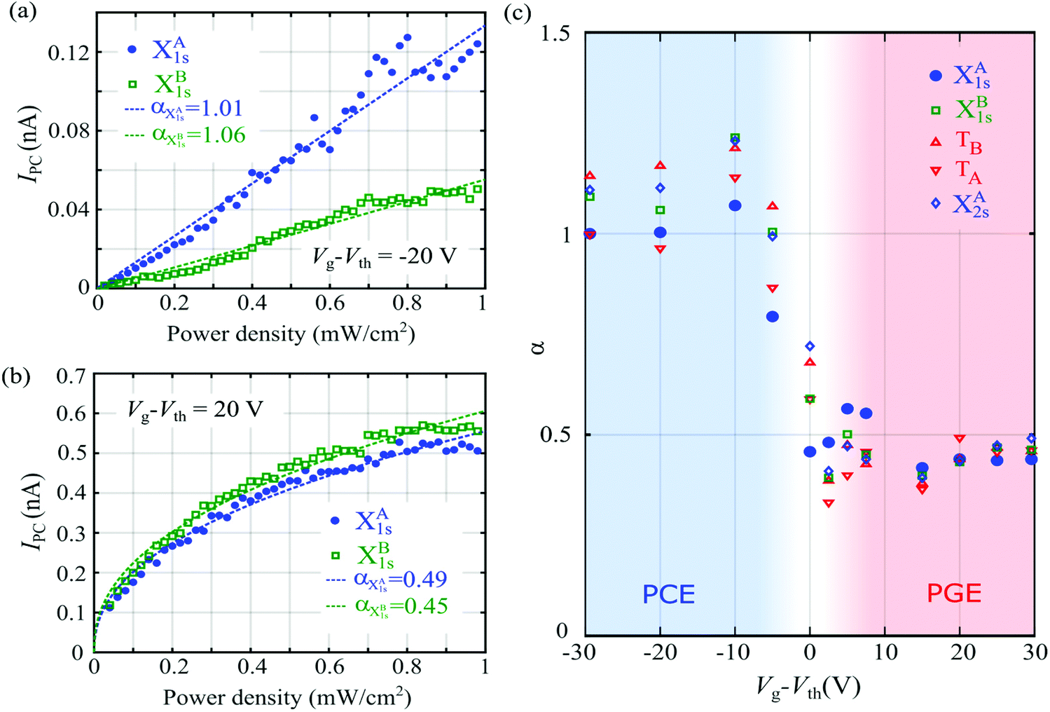 | ||
| Fig. 3 Power dependence of IPC in the two gate voltage regimes. (a) Power dependence of IPC for Vg − Vth = −20 V acquired at two different photon energies E matching the X1sA and X1sB excitonic spectral features of monolayer MoS2. Lines are fittings to IPC ∝PαD with α ≈ 1. (b) Same as (a) for Vg − Vth = 20 V. The fittings now give α ≈ 0.5. (c) Dependence of the fitting parameter α on Vg − Vth, measured for photon energies matching the five main excitonic spectral features of monolayer MoS2. The two different regimes for power dependence, corresponding to the PCE-dominated and the PGE-dominated photoresponse regimes are indicated in the figure. | ||
For gate voltages well above the threshold voltage (Fig. 3b), however, the situation completely changes and the power dependence of IPC becomes sublinear. A typical phenomenological approach used in previous works to distinguish PGE and PCE is to fit the power dependence to IPC ∝ PαD, where α = 1 is generally associated to PCE and α < 1 to PGE. Fig. 3c shows the parameter α extracted from these fittings as a function of the gate voltage for five different illumination energies, matching the five main excitonic transitions of 1L-MoS2, as labelled in the figure and discussed in ESI section S2.† As one can clearly observe in the figure, for gate voltages below Vth we get α ≈ 1, regardless of the selected illumination wavelength, while for Vg > Vth we get α ≈ 0.5. In the next section we discuss the photocarrier dynamics of the system and correlate them with the observed power dependencies.
B.4 Carrier dynamics
Proceeding similarly to earlier literature6,15 we analyse the dynamics of photoexcited carriers using a modified Hornbeck–Haynes model. We consider a scenario where the main photocarrier relaxation mechanism is Shockley–Read–Hall recombination mediated by midgap states. We also include a discrete density of localized states Dt at an energy near the valence band edge to account for the presence of shallow hole traps (see Fig. 4a). In 1L-MoS2 such midgap states and shallow traps are expected to occur due to the presence of sulfur vacancies in the crystal lattice.16–18 For an n-doped semiconductor we can assume that only the hole traps near the valence band are relevant, since electron traps are already filled at equilibrium. For simplicity, we also assume that the characteristic times for decay of electrons and holes to the midgap states are equal, i.e., τe = τh ≡ τr.6 Under these assumptions, the dynamics of the photoexcited carriers are described by: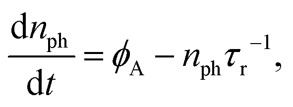 | (6) |
 | (7) |
 | (8) |
 | ||
| Fig. 4 Model for photocarrier dynamics. (a) Schematic drawing of the simplified energy band diagram and excitation/relaxation processes considered in the model. (b) Comparison between fittings of the power dependence of IPC to PαD (black dashed lines) and to our model (eqn (14); red solid lines). | ||
Solving eqn (6)–(8) for the steady state we get:
| pph = ϕAτr, | (9) |
 | (10) |
The presence of hole traps has two main effects in the resulting photoresponse: Firstly, it affects the efficiency of PCE relative to a trap-free scenario. The photoinduced increase of conductance is
| ΔσPCE = q(μn + μp)pph + qμppt, | (11) |
Secondly, the trapped states pt partially screen the electric field arising from Vg, giving an additional contribution to the photocurrent due to the PGE. As we argue below, we believe that this contribution (not considered in earlier literature) is responsible for the fast-response PGE observed experimentally at high light-modulation frequencies.
Following eqn (4), the shift in the threshold voltage due to the trapped charge carriers, pt is given by
 | (12) |
 | (13) |
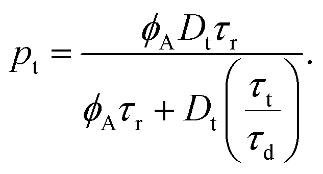
Finally, using eqn (10) we obtain
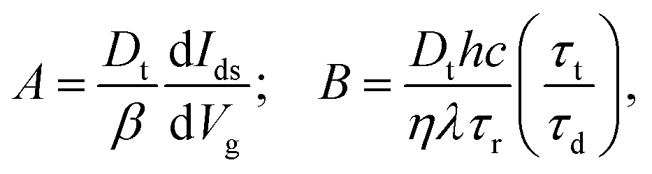
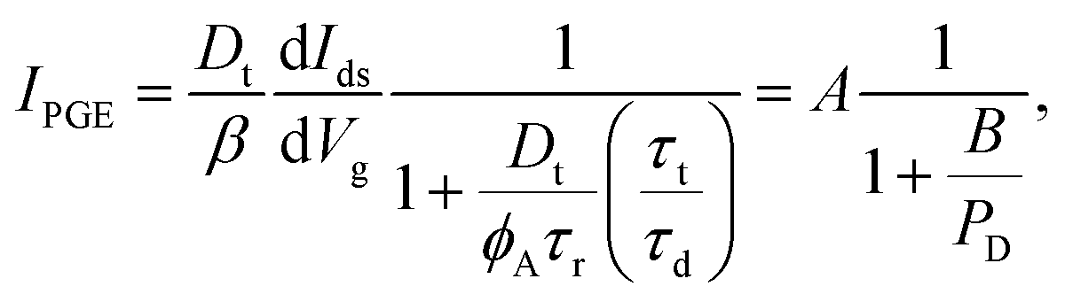 | (14) |
 | (15) |
We now use eqn (14) to fit the measured power dependence for Vg − Vth = 20 V. Fig. 4b shows the measured power dependence of IPC for Vg − Vth = 20 V and its fitting to eqn (14), using A and B as fitting parameters. For comparison, we also show the best fit to the phenomenological equation IPC ∝ PαD, commonly found in literature. While both fitting curves have a similar shape, our model allows us to better reproduce the experimental data points. For the norm of residuals (r) of the fittings to eqn (14) we get rA = 10 pA and rB = 10 pA for excitons XA and XB respectively, roughly twice smaller than the values obtained for the fitting to IPC ∝ PαD (rA = 20 pA and rB = 10 pA). From the obtained fitting parameters A and B we can now extract an estimation for the density of trap states Dt ≈ 1 × 1010 cm−2, as well as the ratio of characteristic times τt(τrτd−1) = 8.5 × 10³ s−1.
Finally, we estimate the energy level associated to the shallow hole traps, ET, over the top of the valence band at EV by considering the detailed balance principle for the transitions between these states. Such condition for this particular case reads6
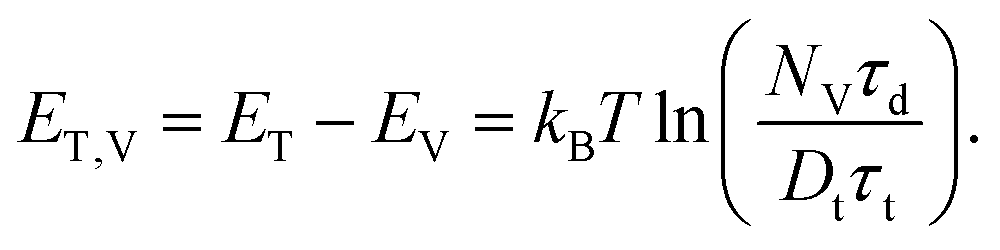 | (16) |
Here kB is the Boltzmann constant and NV is the effective density of states of the valence band, given as NV = gm*KBT/(πℏ2). In our 2D system g = 2 due to the valley degeneracy and the effective mass of the carriers is m* = 0.4m0 with m0 being the free electron mass.22
Last, since there are clear evidences that the recombination time τr is within the order of few picoseconds at low temperature,23,24 we take the value of τr ≈ 5 ps to estimate the energy of the hole traps relative to the top of the valence band as ET,V ≈ 8.4 meV. This finding suggests the existence of shallow hole levels with energy very close to the valence band edge. As discussed below, we associate these levels with the presence of sulfur vacancies in the MoS2 crystal.
C Conclusions
In all, we clearly identified two different regimes for photocurrent generation, that can be distinguished by their different dependence on the illumination power density PD. For Vg < Vth, where the 1L-MoS2 conduction band is fully depleted, IPC is linear with PD, indicating that photocurrent is produced by PCE. In contrast, for Vg > Vth, there are three mechanism contributing to photoresponse: slow-response PGE (most likely due to polar molecules), a fast-response PGE (which we attribute to sulfur vacancies) and a PCE. In this latter case, the power dependence of the photocurrent becomes sublinear, indicating that the two PGE mechanisms are dominant over PCE.In earlier works,6 PGE in 1L-MoS2 devices was attributed to a slow charge-trapping process by polar adsorbates in the vicinity of the 2D channel. However, here we find that the PGE dominates the photoresponse of the device even at frequencies as high as 1 kHz. We attribute this fast PGE to the effect of charge accumulation in shallow impurities near the 1L-MoS2 valence band. By fitting the experimentally observed power dependence of IPC to a modified Hornbeck–Haynes model that includes this effect we can estimate the density of trap states to be Dt ≈ 1 × 1010 cm−2. Thus, even for relatively low trap densities, charge accumulation in shallow impurities can be the dominant mechanism for photoresponse.
The fitting mentioned above also allowed us to estimate the energy of the trap states to be of the order of 8 meV above the valence band edge. We considered different potential origins for these traps, including both native defects in the MoS222 and extrinsic defects such as defects arising due to the h-BN encapsulation.13,25 One of the most common defects in MoS2, especially if it is fabricated by exfoliation, are sulfur vacancies. Ab initio simulations of these defects16–18 indicate that they support the existence of two families of states within the energy gap: a branch of states lying slightly above the middle of the gap, and a second branch lying very close to the valence band edge (which energy depends on the particular set of simulation parameters). Special attention to the latter branch has been paid in ref. 16, where the authors claim that these states present acceptor-like behaviour. Based on this evidence, we believe that the origin of the fast-responding PGE found in this work is related to the presence of sulfur vacancies in the 1L-MoS2 channel.
D Experimental details
D.1 Device fabrication and contact geometry
We use a dry-transfer method based on the use of polypropylene carbonate (PPC) films26 for fabricating the heterostructure of single layer (1L) MoS2 completely encapsulated in hexagonal boron nitride (h-BN). The MoS2 and h-BN flakes are first exfoliated by the standard scotch-tape method and transferred onto SiO2/Si substrate. Then, we use optical microscopy to identify the 1L-MoS2 flakes and confirm their thickness by micro-Raman spectroscopy (see ESI section S5†). We also select two h-BN flakes with thicknesses of 15–20 nm for the top layer h-BN and 25–30 nm for the bottom layer one (determined by their optical contrast).Next, we transfer the top h-BN onto the MoS2 flake and remove the remaining PPC by cleaning the sample with anisole, acetone and isopropanol (IPA) for few minutes. Both flakes are then picked up together with a PPC film and transferred onto the bottom h-BN. Finally, we perform a last cleaning with anisole, acetone and IPA, followed by an annealing in argon to remove any remaining PPC and bubbles in the heterostructure.27
The device geometry is defined by electron beam lithography (EBL) using PMMA as resist. For developing the resist we use a mixture of 1 part MIBK to 3 parts of isopropanol.28 We etch away the EBL-exposed areas by dry plasma etching in a SF6 atmosphere (40 sccm, P = 75 W, process pressure 6 mTorr and T = 10 °C).29 The sides of the resulting etched structure have a pyramidal profile, necessary for a successful fabrication of edge contacts.
After defining the stack geometry, we fabricate the metallic contacts by a second EBL process followed by e-beam evaporation of 5 nm of titanium and 45 nm of gold. To prevent oxidation of the edge contacts all the fabrication steps described above are carried out in a single day. An optical image of the final device is presented in ESI Fig. S5.†
D.2 Electrical and optoelectronic measurements
The measurements are realized while keeping the sample inside a pulse-tube cryostat with an optical access. Drain–source and transfer IV characteristics are measured in two-terminal configuration using a two-channel sourcemeter unit (Keithley 2614B) The light source is a supercontinuum (white) laser (SuperK Compact), and the excitation wavelength is selected using a monochromator (Oriel MS257 with 1200 lines per mm diffraction grid). This allows to scan the visible and NIR spectral range, roughly from 450 nm to 840 nm. For AC optoelectronic measurements, the optical excitation is modulated by a mechanical chopper and the electrical response of the device is registered using a lock-in amplifier (Stanford Research SR830).Author contributions
E. Diez and J. Q. conceived and supervised the research, D. V., Y. M. M., and J. Q. developed and tested the experimental setup for photocurrent spectroscopy. V. C., J. S.-S. and J. Q. fabricated and characterized the monolayer MoS2 phototransistor, D. V. and J. Q. carried out the electronic, optoelectronic, and spectral measurements and data analysis, D. V., J. Q., E. Díaz, L. C. and F. D.-A. performed the theoretical analysis. The article was written through contribution of all the authors, coordinated by J. Q.Conflicts of interest
There are no conflicts to declare.Acknowledgements
We acknowledge financial support from the Agencia Estatal de Investigación of Spain (Grants PID2019-106820RB, RTI2018-097180-B-100, and PGC2018-097018-B-I00) and the Junta de Castilla y León (Grants SA256P18 and SA121P20), including funding by ERDF/FEDER. J. Q. acknowledges financial support from MICINN (Spain) through the programme Juan de la Cierva-Incorporación. We are also thankful to Mercedes Velázquez for her help with the photoluminescence and Raman characterization and to Adrián Martín-Ramos for his assistance on the development of the photocurrent measurement setup.Notes and references
- J. A. G. Sheneve, Z. Butler, S. M. Hollen, L. Cao and Yi Cui, ACS Nano, 2013, 7, 2898–2926 CrossRef PubMed.
- K. F. Mak, K. L. McGill, J. Park and P. L. McEuen, Science, 2014, 344, 1489–1492 CrossRef CAS PubMed.
- H. S. Lee, S.-W. Min, Y.-G. Chang, M. K. Park, T. Nam, H. Kim, J. H. Kim, S. Ryu and S. Im, Nano Lett., 2012, 12, 3695–3700 CrossRef CAS PubMed.
- J. Xiao, M. Zhao, Y. Wang and X. Zhang, Nanophotonics, 2017, 6, 1309–1328 CAS.
- O. Lopez-Sanchez, D. Lembke, M. Kayci, A. Radenovic and A. Kis, Nat. Nanotechnol., 2013, 8, 497–501 CrossRef CAS PubMed.
- M. M. Furchi, D. K. Polyushkin, A. Pospischil and T. Mueller, Nano Lett., 2014, 14, 6165–6170 CrossRef CAS PubMed.
- B. Miller, E. Parzinger, A. Vernickel, A. W. Holleitner and U. Wurstbauer, Appl. Phys. Lett., 2015, 106, 1–5 Search PubMed.
- J. O. Island, S. I. Blanter, M. Buscema, H. S. J. Van Der Zant and A. Castellanos-Gomez, Nano Lett., 2015, 15, 7853–7858 CrossRef CAS PubMed.
- H. Fang and W. Hu, Adv. Sci., 2017, 4, 1700323 CrossRef PubMed.
- H. Huang, J. Wang, W. Hu, L. Liao, P. Wang, X. Wang, F. Gong, Y. Chen, G. Wu, W. Luo, H. Shen, T. Lin, J. Sun, X. Meng, X. Chen and J. Chu, Nanotechnology, 2016, 27, 445201 CrossRef PubMed.
- J. Quereda, T. S. Ghiasi, F. A. van Zwol, C. H. van der Wal and B. J. van Wees, 2D Mater., 2018, 5, 015004 CrossRef.
- D. Kufer and G. Konstantatos, Nano Lett., 2015, 15, 7307–7313 CrossRef CAS PubMed.
- J. Quereda, T. S. Ghiasi, C. H. Van Der Wal and B. J. Van Wees, 2D Mater., 2019, 6(2) DOI:10.1088/2053-1583/ab0c2d.
- A. Epping, L. Banszerus, J. Güttinger, L. Krückeberg, K. Watanabe, T. Taniguchi, F. Hassler, B. Beschoten and C. Stampfer, J. Phys.: Condens. Matter, 2018, 30, 205001 CrossRef PubMed.
- D. Macdonald and A. Cuevas, Appl. Phys. Lett., 1999, 74, 1710–1712 CrossRef CAS.
- X. Zhang, S. Wang, C. K. Lee, C. M. Cheng, J. C. Lan, X. Li, J. Qiao and X. Tao, Phys. Chem. Chem. Phys., 2020, 22, 21776–21783 RSC.
- H. Qiu, T. Xu, Z. Wang, W. Ren, H. Nan, Z. Ni, Q. Chen, S. Yuan, F. Miao, F. Song, G. Long, Y. Shi, L. Sun, J. Wang and X. Wang, Nat. Commun., 2013, 4, 3–8 Search PubMed.
- A. Wu, Q. Song and H. Liu, Comput. Theor. Chem., 2020, 1187, 112906 CrossRef CAS.
- T. Das and J.-H. Ahn, FlatChem, 2017, 3, 43–63 CrossRef CAS.
- A. J. Chiquito, C. a. Amorim, O. M. Berengue, L. S. Araujo, E. P. Bernardo and E. R. Leite, J. Phys.: Condens. Matter, 2012, 24, 225303 CrossRef PubMed.
- J. Quereda, J. J. Palacios, N. Agräit, A. Castellanos-Gomez and G. Rubio-Bollinger, 2D Mater., 2017, 4, 021006 CrossRef.
- W. Zhu, T. Low, Y. H. Lee, H. Wang, D. B. Farmer, J. Kong, F. Xia and P. Avouris, Nat. Commun., 2014, 5, 1–8 Search PubMed.
- T. Korn, S. Heydrich, M. Hirmer, J. Schmutzler and C. Schller, Appl. Phys. Lett., 2011, 99, 2–5 CrossRef.
- M. Palummo, M. Bernardi and J. C. Grossman, Nano Lett., 2015, 15, 2794–2800 CrossRef CAS PubMed.
- M. T. Greenaway, E. E. Vdovin, D. Ghazaryan, A. Misra, A. Mishchenko, Y. Cao, Z. Wang, J. R. Wallbank, M. Holwill, Y. N. Khanin, S. V. Morozov, K. Watanabe, T. Taniguchi, O. Makarovsky, T. M. Fromhold, A. Patanè, A. K. Geim, V. I. Fal, K. S. Novoselov and L. Eaves, Commun. Phys., 2018, 1(94) DOI:10.1038/s42005-018-0097-1.
- M. Caridad, L. Wang, J. Hone, F. Pizzocchero, L. Gammelgaard, B. S. Jessen, P. Bøggild, T. J. Booth, J. M. Caridad, L. Wang, J. Hone, P. Bøggild, T. J. Booth, L. Wang, J. Hone, P. Bøggild and T. J. Booth, Nat. Commun., 2016, 7, 11894 CrossRef PubMed.
- D. G. Purdie, N. M. Pugno, T. Taniguchi, K. Watanabe, A. C. Ferrari and A. Lombardo, Nat. Commun., 2018, 9, 5387 CrossRef CAS PubMed.
- M. McCord and M. Rooks, Electron Beam Lithography, Handbook of microlithography, micromachining, and microfabrication, SPIE, Microlithography 1, 1997, ch. 2, vol. 1 Search PubMed.
- V. Clericò, J. A. Delgado-Notario, M. Saiz-Bretín, A. V. Malyshev, Y. M. Meziani, P. Hidalgo, B. Méndez, M. Amado, F. Domínguez-Adame and E. Diez, Sci. Rep., 2019, 9, 13572 CrossRef PubMed.
Footnote |
| † Electronic supplementary information (ESI) available: PDF file with supplementary notes on experimental details and the estimation of carrier densities. See DOI: 10.1039/d1nr03896f |
| This journal is © The Royal Society of Chemistry 2021 |