DOI:
10.1039/D1NR03440E
(Paper)
Nanoscale, 2021,
13, 15611-15623
Theoretical investigations of novel Janus Pb2SSe monolayer as a potential multifunctional material for piezoelectric, photovoltaic, and thermoelectric applications†
Received
29th May 2021
, Accepted 6th August 2021
First published on 31st August 2021
Abstract
Two-dimensional Janus nanomaterials, due to their unique electronic, optical, and piezoelectric characteristics resulting from the antisymmetric structures, exhibit great prospects in multifunctional energy application to alleviate the energy crisis. Monolayer Janus Pb2SSe, with a black phosphorus-like structure and an indirect band gap of 1.59 eV as well as high carrier mobility (526–2105 cm2 V−1 s−1), displays outstanding potentials in the energy conversion between nanomechanical energy, solar energy, waste heat, and electricity, which has been comprehensively studied utilizing DFT-based simulations. The research results reveal that monolayer Pb2SSe not only possesses giant in-plane piezoelectricity of d11 = 75.1 pm V−1 but also superhigh out-of-plane piezoelectric coefficients (d31 = 0.5 pm V−1 and d33 = 15.7 pm V−1). Meanwhile, by constructing Pb2SSe bilayers, the out-of-plane piezoelectric coefficients can be significantly enhanced (d31 = 19.2 pm V−1 and d33 = 194.7 pm V−1). In addition, owing to the small conduction band offset, suitable donor band gap and excellent light absorption capability in the Pb2SSe/SnSe (Pb2SSe/GeSe) heterostructure, the power conversion efficiencies were calculated to be up to 20.02% (Pb2SSe/SnSe) and 19.28% (Pb2SSe/GeSe), making it a promising candidate for solar energy collection. Furthermore, from the thermoelectric electron and phonon transport calculations, it can be found that the Pb2SSe monolayer is an n-type thermoelectric material with ultrahigh ZT = 2.19 (1.52) at room temperature, which can be traced back to its ultralow κL = 0.78 (0.99) W m−1 K−1, and superhigh PF = 10.18 (8.25) mW m−1 K−2 along the x(y) direction at the optimal doping concentration at 300 K. The abovementioned versatile characteristics in the Janus Pb2SSe monolayer, along with its comprehensive stabilities (energy, dynamic, thermal, and mechanical stabilities), highlight its potential in clean energy harvesting.
1. Introduction
The growing demand of high-efficiency clean energy has aroused the need for new technologies that are able to utilize multi-aspect clean energy or improvement the energy efficiency of traditional methods to cope with the energy crisis and avoid further environmental degradation.1,2 Soon after the groundbreaking discovery of the ultrathin carbon sheet graphene, two-dimensional (2D) nanomaterials have gained unprecedented interest in the past decades. Their unique physical properties, derived from the quantum confinement effects that are lacking in the bulk counterparts,3 provide great opportunities in the development of next-generation energy conversion applications. Graphene, with excellent mechanical properties, ultrahigh thermal conductivity, and extremely high carrier mobility, has been industrialized and extensively used in energy reserves4,5 but its zero-band gap characteristic also limits its application in some fields.6 Subsequently, 2D materials h-BN,7 phosphorene,8 transition metal sulfides (TMDs),9 Mxene,10 and so forth,11,12 have been broadly reported in theory and experiment, showing a wide range of energy utilization prospects. However, these 2D materials, due to their intrinsic single characteristics, usually fail to meet the increasing demand in multi-field energy applications. Very recently, the asymmetric 2D Janus structures, displaying several novel properties that are not present in the original monolayers, have been gaining extensive popularity. In experiment, since the Janus MoSSe monolayer has been firstly successfully fabricated by replacing the top layer of Se atoms in MoSe2 by S atoms,13 more other analogous Janus monolayers such as WSSe and PtSSe monolayers14,15 were synthesized by the chemical vapor deposition (CVD) approach. In theory, various Janus structures are widely studied and show great potential for collecting clean energy from renewable energy resources, including mechanical energy, solar energy, and waste heat by piezoelectricity, photovoltaics, and thermoelectricity.16–18
Since MoS2 monolayer has been theoretically and experimentally demonstrated to have a strong in-plane piezoelectric coefficient (d11 ∼3.0 pm V−1),19,20 which is larger than that of commercial bulk α-quartz (2.3 pm V−1),21 increasing interest has been given to seeking other 2D piezoelectric materials in the recent years. For example, giant piezoelectric values (d11 = 75.43–250.58 pm V−1) in the group IV–VI monolayers and superhigh piezoelectric coefficients (0.67–243.45 pm V−1) in group V binary compounds have been reported.22,23 Particularly, in comparison with the common 2D monolayers, Janus monolayers, due to the damaged inversion symmetry and out-of-plane mirror symmetry, not only display large in-plane coefficients but also extra out-of-plane polarization. The 2D Janus TMDs (MXY), which have been theoretically first reported by Shenoy et al.,24 exhibit large in-plane piezoelectric coefficients (2.3–5.3 pm V−1). Surprisingly, the out-of-plane piezoelectric coefficient of bilayer MoSTe can even reach 13.5 pm V−1, which is superior to the bulk piezoelectric solids, such as wurtzite-GaN (d33 = 3.1 pm V−1). Recently, Ahammed et al.21 predicted that 2D Janus monolayers and bilayers of group IV transition-metal trichalcogenides possess extremely high in-plane and out-of-plane piezoelectric values (d11 = 8.19 pm V−1 and d33 = 68.72 pm V−1). Furthermore, the Janus group III chalcogenide monolayers and Te2Se monolayer have also been predicted to show high piezoelectric polarization.25,26 Janus structures show great advantages in electromechanical energy conversion, highlighting their future application in nanopiezotronics.
Building 2D van der Waals (vdW) heterostructures composed of donor and acceptor semiconductors has been considered as a promising method to design efficient photovoltaic (PV) cells to utilize clean solar energy. Li et al.27 reported a graphene/GaAs vdW heterostructure solar cell, adopting a designed graphene–dielectric–graphene gating structure, and the power conversion efficiency (PCE) can reach 18.5%, which is superior to that of traditional copper zinc tin sulfoselenide (CZTSSe) of 12.6%.28 In addition, studies of the applications of ultrathin heterostructure PV cells based on neoteric 2D materials (such as TMDs, phosphorene, tellurene, and GeSe monolayers), are widely explored in theory owing to their intrinsic favorable direct band gaps.29–32 Interestingly, for the 2D Janus vdW structures, the intrinsic built-in electric field will efficiently promote the transfer and separation of the photogenerated carriers and extend the carrier lifetimes, which will facilitate the utilization of sunlight and improve the photoelectric conversion efficiency.33,34 For instance, the Janus 2D MoSSe/BX (X = P, As) heterostructures show ultrahigh excitonic solar conversion efficiencies (22.97% and 20.86%) due to the extremely small conduction band offset.35 In addition, the ultrathin heterostructure PV cells composed of Janus TMDs monolayers exhibits high excitonic solar efficiencies ranging from 15% to 20%.16 Thus, the heterostructure PV cells based on the Janus structures show a great prospect of harvesting solar energy.
Low-dimensional materials show better thermoelectric (TE) performances than their bulk counterparts owing to the outstanding electronic and phonon transport properties, which can be traced back to the quantum confinement effect.36 Huang et al.37 theoretically investigated monolayer Mg3Sb2, exhibiting high thermoelectric ZT of 2.5 at 900 K, which is larger than that of the bulk (ZT = 1.8). N-type Bi2O2Se nanosheets, proposed by Yu et al.,38 displays a high ZT (3.35) in n-type doping at 800 K, which is much larger than that of the bulk Bi2O2Se (0.2). In particular, for Janus structures, because of the breakdown of the inversion symmetry, the phonon scattering rate will increase compared with the pristine monolayers, resulting in the reduction of the lattice thermal conductivity. For example, the intrinsic lattice thermal conductivity of the Janus ZrSSe monolayer at 300 K is 1.68 W m−1 K−1, and it is only 70% of the ZrS2 monolayer (2.39 W m−1 K−1), which can be attributed to its shorter phonon lifetime and smaller group velocities of the ZrSSe monolayer.39 In addition, owing to the variation of the electronic structure, the electronic transport properties of the Janus structures will be different from the pristine monolayers. It has been proved that the values of the Seebeck coefficient, carrier mobility, and electrical conductivity of the Janus WSSe monolayer exceeds those of the WS2 monolayer.9 Therefore, it can be anticipated that the thermoelectric performance will be improved when the previous excellent 2D TE materials become Janus structures.
Based on these advances, the Janus structures show great potential in multifunctional energy devices due to their superior performance to the original monolayers in many aspects. Group IV–VI monochalcogenides family,40 having unique structures similar to black phosphorus, suitable band gap, and satisfactory carrier mobility (∼103 cm2 V−1 s−1), show superior mechanical flexibility, high optical absorption capability, and large electronic transport coefficient,41,42 which open up a new possibility to construct Janus structures for energy utilization. In this work, on the basis of DFT simulations, we theoretically report a novel group IV–VI Janus Pb2SSe monolayer, which can be obtained by displacing one S atom in the PbS monolayer to the Se atom using CVD. The all-round dynamic, thermal, and mechanical stabilities of the Pb2SSe Janus monolayer have been demonstrated by checking its phonon dispersion, ab initio molecular dynamics, and elastic constants. Monolayer Pb2SSe, with an anisotropic structure, shows an indirect band gap of 1.59 eV and superhigh carrier mobility (526–2105 cm2 V−1 s−1) as well as high mechanical flexibility. In order to explore the prospect of energy conversion, in-depth studies on the piezoelectric properties of monolayer and multilayer heterostructures, and the solar energy conversion efficiency of the constructed heterostructures along with the thermoelectric properties have been theoretically employed. The obtained appealing properties including superhigh in-plane (d11 = 75.1 pm V−1) and out-of-plane (d31 = 19.2 pm V−1 and d33 = 194.7 pm V−1) piezoelectric coefficients, over 20% excitonic solar conversion efficiency, and high ZT (2.19) at room temperature, highlight its promising multifunctional application in energy harvesting.
2. Computational details
First-principles computations on the basis of density functional theory (DFT) have been employed in this work, adopting the Vienna ab initio simulation package (VASP).43 The exchange–correlation potential in the form of Perdew–Burke–Ernzerhof (PBE) generalized-gradient approximation (GGA) was applied.44,45 We have adopted the projector-augmented plane wave (PAW) pseudopotential approach with a cutoff of 520 eV to describe the ion–electron interactions.46 To obtain more elaborate electronic band structures, the Heyd–Scuseria–Erzenhof functional (HSE06)47 method was employed and the spin-orbital coupling (SOC) effect was considered due to Pb being a rather heavy element. The DFT-D3 approach was used to correct the van der Waals interactions between the heterostructures and the bilayers.48 The force criterion and energy convergence conditions as well as k-meshes were found to be 10−3 eV Å−1, 10−6 eV, and 9 × 9 × 1 for geometry optimization. In addition, a dense k-mesh of 12 × 11 × 1 was used for electron-related calculations. In order to calculate the piezoelectric coefficients, density functional perturbation theory (DFPT) was used.49 The phonon dispersion and second-order interaction force constants (2nd IFCs) were obtained by phonon-finite-displacement with 6 × 6 × 1 supercell in the Phonopy code.50 The third-order force constants (3rd IFCs) were extracted by the thirdorder.py code with the 4 × 4 × 1 supercell and an interaction range of 6.3 Å was chosen for the 3rd IFCs calculation. According to 2nd IFCs and 3rd IFCs, the lattice thermal conductivity was obtained using the ShengBTE code.51 The electronic transport properties were studied by the BoltzTraP2 code with the 45 × 44 × 1 k-mesh52 on the basis of the Boltzmann transport equation (BTE).
3. Results and discussion
3.1 Structure and stability
The pristine cell of the bulk Pb2SSe crystal, which has been synthesized by the mixture of PbS and PbSe crystals,53,54 has a cubic structure with the P4/mmm space group, as illustrated in Fig. 1(a). The optimized bulk Pb2SSe crystal constant is equal to 4.325 Å, and the bond length of Pb–S(Se) is 3.06 Å. Next, we obtained the Janus monolayer Pb2SSe by cleaving the (0 0 1) plane of the Pb2SSe cell, which exhibits a double atomic layer and a rectangular structure similar to the SnSe and GeSe monolayers,55 as displayed in Fig. 1(b). The Janus Pb2SSe monolayer, owing to the lack of the inversion symmetry, shows the Pm space group, which is less symmetric than the PbS and PbSe monolayers (P4/nmm).56,57 Each unit cell consists of one S, one Se, and two Pb atoms with four alternating atoms connected in the order of Pb–Se–Pb–S. The fully relaxed Pb2SSe monolayer shows anisotropic lattice parameters (a = 4.373 Å and b = 4.326 Å), and the bond lengths (l1, l2) for Pb–S and the bond lengths (l3, l4, l5) for Pb–Se are listed in Table 1. To clearly study the bonding characteristic in the Pb2SSe monolayer, the electron localization function (ELF) is presented in Fig. 1(c). It can be noted that both the Pb–S and Pb–Se bonds show weak localization and the contour values of ELF are nearly 0.2–0.3, suggesting weak covalent bonding and the presence of typical ionic bond properties in the Pb2SSe monolayer.32 More information about their bonding character is deducible from the crystal orbital Hamilton population (COHP) analysis, as implemented in the LOBSTER package,58 and the average COHP curves is displayed in Fig. S1.† Antibonding and bonding interactions correspond to the negative and positive energy regions of the COHP curve, respectively. It can be observed that near the bonding states of CBM, the Pb–S bond interaction in the Pb2SSe monolayer is stronger than that in the PbS monolayer, while the Pb–Se bonding state is lower than that in the PbSe monolayer. The trends in the COHP curve can be further verified by the larger integrated COHP (ICOHP) value of −2.92 eV in the Pb–S bond and the lower value of −1.21 eV in the Pb–Se bond, as presented in Table S1.† Such complicated configuration and relatively weak chemical bonds are conducive for promoting phonon scattering and inhibit the heat transport. In addition, we performed the computation about the cohesive energy of the Pb2SSe monolayer to validate energy stability utilizing the formula Ecoh = [EPb2SSe − (2EPb + ES + ESe)]/4, in which Ecoh represents the average cohesive energy per atom; EPb2SSe, EPb, ES, and ESe stand for the total energy of the unit cell of Pb2SSe, isolated Pb, S, and Se atoms, respectively. The calculated cohesive energy is 4.13 eV per atom, which is larger than that of germanene (3.26 eV per atom), Janus monolayer In2SeO (3.76 eV per atom), and silicene (3.98 eV per atom),59,60 suggesting the reliable energetic stability and high preparative feasibility of the Pb2SSe monolayer. The thermodynamic stability of monolayer Pb2SSe was evaluated by the formation energy (ΔEf) and the energy above the hull value (ΔHhull), according to eqn (S1) and (S2).† The obtained ΔEf is 62.7 meV per atom, which is much lower than the threshold formation value of 200 meV per atom for experimental preparation, and the calculated ΔHhull is −0.098 eV per atom, which is slightly lower than −0.06 eV per atom of the SnSSe monolayer,61 corroborating the high thermodynamic stability of monolayer Pb2SSe.
 |
| | Fig. 1 (a) Structural characterization of bulk Pb2SSe. (b) The plane and lateral views of the atomic structure of monolayer Pb2SSe, and the primitive cell is enclosed by a red dotted line. (c) The electron localization function profile of monolayer Pb2SSe along the side of Se atoms and S atoms. | |
Table 1 Lattice parameters (a and b) Å, bond lengths (l1, l2, l3, l4 and l5) Å, and band gap at the PBE, HSE06, PBE + SOC, and HSE06 + SOC level (Epbe, Ehse, Epbe+soc, and Ehse+soc) eV
| Structure |
a
|
b
|
l
1
|
l
2
|
l
3
|
l
4
|
l
5
|
E
pbe
|
E
hse
|
E
pbe+soc
|
E
hse+soc
|
| Pb2SSe |
4.373 |
4.326 |
2.704 |
3.036 |
2.821 |
3.114 |
2.919 |
1.43 |
1.99 |
1.05 |
1.59 |
Furthermore, the dynamic stability of monolayer Pb2SSe was investigated by carrying out phonon spectrum calculation, as shown in Fig. 2(a). It can be noted that, in the first Brillouin zone, free negative frequency can be observed, confirming its dynamic stability. Specifically, all high-frequency optical branches have frequencies less than 7 THz, and low-frequency acoustic branches are less than 1.5 THz, which are smaller than many excellent monolayer thermoelectric materials.62,63 In addition, in PDOS analysis, it was found that the high-frequency acoustics are mainly dominated by the S element and the low-frequency optics and acoustics are primarily given by Pb and Se elements. Then, we used ab initio molecular dynamics (AIMD) simulations to explore the thermal stability of the Pb2SSe monolayer at 700 K. Through the simulation of 10 ps, as shown in Fig. 2(b), the fact that the fluctuation of the free energy converges to a constant and the supercell of 5 × 5 × 1 of the Pb2SSe monolayer remains relatively intact proves that it has good thermal stability. Furthermore, considering that the mechanical stability is an indispensable term for the practical application of 2D materials, the mechanical stability of the Pb2SSe monolayer has also been established by conformation to the Born–Huang stability criteria, as presented in Table S2.†
 |
| | Fig. 2 (a) Phonon spectrum and partial density-of-states (PDOS) of monolayer Pb2SSe. (b) The free energy as a function of the AIMD simulation time and the final structures of monolayer Pb2SSe at 700 K. | |
3.2 Electronic and transport properties
Without the consideration of spin–orbit coupling (SOC), the Pb2SSe monolayer displays semiconductor behavior with quasi-direct band gaps of 1.43 eV and 1.99 eV at the PBE and HSE06 levels, as shown in Fig. S2(a) and (b).† Both the VBM and CBM are near the X point. When turning on SOC, the CBM will move from the X point to the Y point, while the VBM is preserved well. Meanwhile, the band gap will show decrements from 1.43 to 1.05 eV at the PBE level and from 1.99 to 1.59 eV using HSE06 functional, as displayed in Fig. S2(c) and (d).† Furthermore, to get more insight into the electronic band structure of the Pb2SSe monolayer, the element-projected band structure and the corresponding PDOSs are displayed in Fig. 3(a). It can be found that the CBM is mainly dominated by the p orbital of the Pb element, while the VBM is contributed by the p orbital of Se and S elements as well as the s orbital of the Pb element. Therefore, the significant changes in the band structure with (without) considering the SOC effect can be inferred, which are mainly arising from the strong SOC strength within the Pb atom in the Pb2SSe monolayer. Interestingly, under biaxial tensile strain varying from 1% to 3%, the band structure of the Pb2SSe monolayer will change from an indirect to a direct semiconductor, which is beneficial for improving the light absorption and photovoltaic application of the material. In Fig. 3(b), as the tensile strain increases from 1% to 5%, the band gap will increase from 1.59 to 2.06 eV, while it shows a decrease from 1.59 to 1.22 eV when the monolayer was subjected to 1%–5% biaxial compressive strain. The fact that the biaxial strain is in good quadratic agreement with the energy per atom demonstrates that all the strains considered are within the elastic limit and that the Pb2SSe monolayer is flexible.
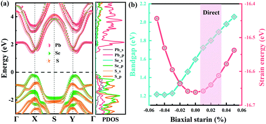 |
| | Fig. 3 (a) The element-projected band structure and the corresponding partial density-of-states (PDOS) of monolayer Pb2SSe using HSE06 functional with the consideration of the SOC effect. (b) The computed band gap and the inner-layer strain energy of the Pb2SSe monolayer with respect to the applied biaxial strains. | |
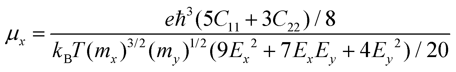
For the purpose of nanopiezoelectric, photovoltaic, and thermoelectric application, the carrier transport properties of the Pb2SSe monolayer are vital factors that can quantitatively evaluate the capability of transport of electrons/holes along specific directions. In this work, utilizing the modified formula within the framework of the deformation potential (DP) theory, which is based on effective mass approximation and an electron–acoustic phonon scattering mechanism,64 the carrier mobility (μ) of the Pb2SSe monolayer along the x and y directions can be evaluated by the following formulas.
| |  | (1) |
| |  | (2) |
in which
C = (∂
2E/∂
δ2)/
S represents the elastic module for the 2D material,
δ,
E, and
S are the uniaxial strain, total energy, and the area of the relaxed unit cell, respectively.
m* =
ħ2/(∂
2ε/∂
k2) stands for the effective mass, and
ε and
k are the band energy and electron wave vector, respectively.
Ed = d
Eedge/d
δ is the DP constant, and
Eedge is the energy of the band edge.
kB,
T, and
ħ are constants, representing the Boltzmann constant, room temperature, and Planck's constant, respectively. As listed in
Table 2, it can be found that both the electron and hole possess superlight effective masses, which agrees well with their dispersive band structures. Interestingly, the Pb
2SSe monolayer shows high electron mobility along the
x direction, up to 2105 cm
2 V
−1 s
−1, which is close to that along the
y direction (1831 cm
2 V
−1 s
−1). In addition, the hole mobilities along the
x and
y directions are 603 and 526 cm
2 V
−1 s
−1, respectively, which are larger than that of the well-known MoS
2 and WS
2 monolayers (<200 cm
2 V
−1 s
−1), respectively. The high carrier mobility (526–2105 cm
2 V
−1 s
−1) of the Pb
2SSe monolayer lays a solid foundation for high performance nanopiezoelectric, photovoltaic, and thermoelectric devices.
Table 2 The electronic transport parameters of monolayer Pb2SSe: effective mass (m*), elastic moduli (C), deformation potentials (Ed), carrier mobility (μ), and carrier relaxation time (τ)
| Direction |
Carrier type |
m*/m0 |
C (N m−1) |
E
d (eV) |
μ (cm2 V−1 s−1) |
τ (fs) |
|
x
|
e |
0.159 |
34.10 |
3.01 |
2105 |
209 |
| h |
0.227 |
34.10 |
3.62 |
603 |
85 |
|
y
|
e |
0.147 |
45.13 |
5.60 |
1831 |
168 |
| h |
0.195 |
45.13 |
8.01 |
526 |
64 |
3.3 Mechanical properties and electromechanical energy conversion
The mechanical performance of a material, which can be described by Young's moduli (Y) and Poisson's ratio (ν), is of significance for designing flexible electronic devices. The orientation-dependent Young's modulus Y(θ) and Poisson's ratio v(θ) can be computed using eqn (S3) and (S4),† and the results are illustrated in Fig. 4(a) and (b). The different anisotropic behaviors of the Pb2SSe monolayer can be clearly seen from anisotropic Y(θ) and v(θ). Obviously, the Young's modulus exhibits the minimum value (24.5 GPa) along the axis, and the maximum value (33.5 GPa) can be realized along the diagonal direction. This value is much lower than that of the most reported 2D material (such as graphene (342.2 GPa), MoS2 (199 GPa), and BP (70 GPa)),65,66 implying its low stiffness and high flexibility. Meanwhile, Poisson's ratio shows remarkable anisotropy and its value ranges from 0.27 to 0.62, uncovering that the Pb2SSe monolayer exhibits excellent flexibility. Such flexible and anisotropic properties could be traced back to the special arrangement between the Pb, Se, and S atoms in the Pb2SSe monolayer, which provides the possibility for the Pb2SSe monolayer to be applied in flexible devices.
 |
| | Fig. 4 The (a) Young's modulus Y(θ) and (b) Poisson's ratio υ(θ) with respect to the orientation. (c) Planar average of the electrostatic potential energy of the Janus Pb2SSe monolayer. (d) The Janus Pb2SSe multilayer structures with four high-symmetry stacking sequences. | |
Further, the piezoelectric effects of monolayer and bilayer Pb2SSe have been investigated to explore its promise in piezoelectric applications. The piezoelectric strain tensor dij was calculated by the well-known formula24
in which
i = 1, 2, and 3 stands for the
x,
y, and
z direction for 2D materials, respectively.
eik is the piezoelectric stress tensor, calculated by the density functional perturbation theory (DFPT).
Cjk is the elastic stiffness coefficient, obtained by fitting the DFT-computed unit-cell energy (
E) to a series of 2D strain states (
ε11,
ε22), based on the following formula.
| |  | (4) |
where
S0 is the area of the unit-cell at zero strain. Specifically,
eqn (3) can be written as
| |  | (5) |
and the calculated values for
eik,
Cjk, and
dij of monolayer Pb
2SSe are shown in
Table 3. It can be found that the Pb
2SSe monolayer exhibits superhigh in-plane piezoelectric coefficient
d11 up to 75.1 pm V
−1. Such a large value is about 20 times larger than the commercial bulk piezoelectric materials such as α-quartz (
d11 = 2.3 pm V
−1). Meanwhile, this value is also much larger than the currently theoretically reported 2D Janus monolayers (such as MoSSe (
d11 = 3.76 pm V
−1),
24 In
2SSe (
d11 = 8.47 pm V
−1),
25 and Te
2Se (
d11 = 16.29 pm V
−1)
26) and is even comparable to that of group IV monochalcogenide monolayers (
d11 = 75.43–250.58 pm V
−1)
22 and group V binary compounds (0.67–243.45 pm V
−1).
23 Thus, the Pb
2SSe monolayer shows high mechanic-electrical energy converting ratio, which can be ascribed to its superhigh piezoelectric stress tensor (
e11 = 2389.9 pC m
−1) and low elastic coefficient (
C11 = 34.1 GPa). In addition, due to the mirror asymmetry structure, it is engaging to find that the Janus Pb
2SSe monolayer possesses out-of-plane piezoelectric coefficients (
d31 and
d33), implying that the out-of-plane piezoelectric effect can be induced by exerting an in-plane uniaxial strain. The calculated values of
d31 = 0.5 pm V
−1 and
d33 = 15.7 pm V
−1 are much larger than those of the 2D Janus MXY monolayers and group III Janus chalcogenide monolayers.
24,25 In order to identify the underlying mechanism of such high out-of-plane piezoelectric coefficient, we present the planar average electrostatic potential energy in
Fig. 4(c). There is an electrostatic potential gradient (Δ
Φ) of about 0.11 eV, resulting from the mirror asymmetrical Janus structure. As shown in Fig. S3,
† it can be clearly found that there are about 0.16|
e| electrons transferring from the sides of the Se atoms to S atoms, leading to a net electric field from the sides of the Se atoms to S atoms. The obtained magnitude of the net electric field and dipole moment are 0.508 eV Å
−1 and 0.05 e Å, respectively, demonstrating the strong out-of-plane polarization in the Pb
2SSe monolayer.
Table 3 The relaxed-ion elastic constants Cij (GPa) and the relaxed-ion piezoelectric coefficients eij (pC m−1) and dij (pm V−1) of the unit cell in the Janus Pb2SSe monolayer and bilayers
| Structure |
C
11
|
C
12
|
C
13
|
C
33
|
e
11
|
e
31
|
e
33
|
d
11
|
d
31
|
d
33
|
| Pb2SSe |
34.1 |
20.9 |
1.7 |
1.0 |
2389.9 |
−0.6 |
−8.5 |
75.1 |
0.5 |
−15.7 |
| I |
68.5 |
42.7 |
0.4 |
1.8 |
5017.6 |
−651.3 |
−213.6 |
88.7 |
19.2 |
−72.8 |
| II |
62.3 |
40.1 |
2.2 |
1.8 |
5024.9 |
−91.2 |
−554.2 |
95.8 |
14.1 |
−194.7 |
| III |
69.9 |
41.7 |
1.6 |
2.1 |
4317.1 |
−124.8 |
−67.7 |
74.0 |
5.4 |
−24.0 |
| IV |
70.2 |
42.9 |
3.8 |
1.9 |
4531.4 |
−49.9 |
−82.9 |
82.6 |
3.4 |
−55.4 |
Considering the relatively weak out-of-plane piezoelectric coefficients in comparison with its in-plane counterpart, we further explored the piezoelectric performances of the Janus Pb2SSe bilayer structures, which are constructed by stacking Janus monolayers without offsetting the out-of-plane piezoelectricity. According to different stacking sequences and orientations, four possible configurations are taken into consideration, where the sides of the Se atoms are always above the sides of the S atoms. From the optimized structural parameters and the binding energies of the four structures, as listed in Table S3,† the stacking-I possesses the lowest binding energy of −81.21 meV Å−2 among the four configurations and its phonon dispersion and AIMD simulation (Fig. S4†), further validating its all-round stabilities. The piezoelectric coefficients of the four configurations are listed in Table 3. It can be noted that the values of d11 of the bilayer Pb2SSe range from 74.0 to 95.8 pm V−1, which are very close to that of monolayer Pb2SSe (75.1 pm V−1), implying that the interlayer vdW interactions produce few influences on the in-plane piezoelectric polarization of each slab. Moreover, it is interesting to find that the out-of-plane coefficient d31 of bilayer Pb2SSe increases nearly 10 times compared with monolayer (0.5 pm V−1), ranging from 3.4 to 19.2 pm V−1 and d33 also shows a large increase and the maximum value is up to 194.7 pm V−1. Such high values are much larger than that of Janus multilayer MoSTe (d31 = 1.23 pm V−1 and d33 = 13.52 pm V−1) and multilayer Janus Te2Se (d31 = 15.9 pm V−1 and d33 = 89.34 pm V−1).24,26 The fact that the out-of-plane piezoelectric coefficients (d31 and d33) are greatly improved by multi-layer regulation demonstrates that the vdW interactions show significant effects on the out-of-plane piezoelectric polarizations. Therefore, it is highly desirable that the Janus Pb2SSe multilayers show great promise for multifunctional piezoelectric applications due to their superhigh in-plane and out-of-plane piezoelectric coefficients.
3.4. Excitonic solar cell and optical properties
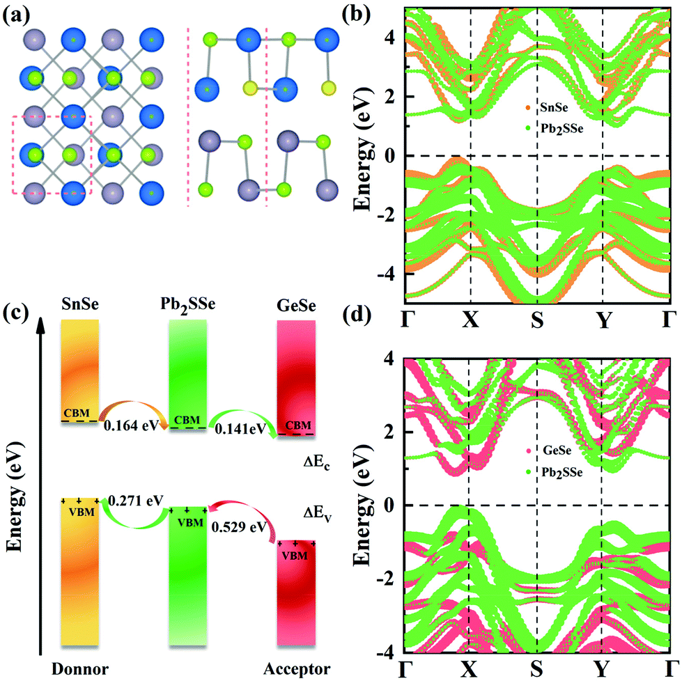
In order to realize the efficient utilization of unlimited solar energy, constructing heterostructures based on 2D materials is regarded as a prospective strategy for next-generation solar cells. In view of this, monolayer Pb2SSe has a suitable band gap of 1.59 eV to benefit solar radiation absorption and high carrier mobility to facilitate carrier migration; two appropriate and lattice-matching 2D materials (GeSe and SnSe monolayers) are used to build heterostructures with the Pb2SSe monolayer to explore its potential in solar cells. Through structural optimization, we got the SnSe slab with the lattice constants a = 4.39 Å and b = 4.29 Å, and a = 4.29 Å and b = 4.01 Å in the GeSe monolayer, respectively, which are well in line with earlier literature.55 For the vertical Pb2SSe/SnSe and Pb2SSe/GeSe heterostructures, there exist eight possible typical stacking configurations, as illustrated in Fig. S5.† The structural parameters such as the lattice parameters, interlayer binding energies, and interlayer distances of these optimized configurations are summarized in Table S4.† Obviously, stacking-c and stacking-C shown in Fig. 4(a) possess the lowest binding energies of −27.18 and −21.30 meV Å−2, which are much larger than the typical vdW crystals such as graphite (−12 meV Å−2),67 indicating their strong energy stability. In addition, the dynamic and thermal stabilities of stacking-c and stacking-C heterostructures were verified by performing phonon dispersion calculations and AIMD simulations with 5 ps at 300 K, as shown in Fig. S6.†
We then investigate the electronic properties of Pb2SSe/SnSe and Pb2SSe/GeSe heterostructures. The band structures of individual SnSe and GeSe monolayers show an indirect band gap of 1.37 eV and a direct band gap of 1.52 eV, respectively, using HSEO6 functional with an SOC effect, as illustrated in Fig. S7(a) and (b).† The projected band structures of Pb2SSe/SnSe and Pb2SSe/GeSe heterostructures are displayed in Fig. 5(b) and (d). It can be found that both Pb2SSe/SnSe and Pb2SSe/GeSe are indirect band gap semiconductors of 1.22 eV and 1.01 eV, respectively. Moreover, both Pb2SSe/SnSe and Pb2SSe/GeSe present typical type-II vdW band alignments, embodied in which the VBM and CBM are contributed by different monolayers. It has been established that such characteristics in the band structures will spontaneously separate the free holes and electrons, which will improve the utilization of photogenerated carriers. A schematic of the band edges of the Pb2SSe/SnSe and Pb2SSe/GeSe heterostructures is plotted in Fig. 5(c), computed from the electronic band structures utilizing the HSEO6 functional with the SOC effect. It can be observed that the valence band offset (VBO) (ΔEv) and the conduction band offset (CBO) (ΔEc) between the isolated monolayers are 0.271 eV (0.529 eV) and 0.164 eV (0.141 eV) for Pb2SSe/GeSe and Pb2SSe/SnSe, respectively. Combining the calculations of planar-averaged charge density difference in Fig. S8† as well as work functions in Table S5,† it can be inferred that the electrons will flow from the SnSe monolayer to Pb2SSe for the Pb2SSe/SnSe heterostructure and from the Pb2SSe to the GeSe monolayer for the Pb2SSe/GeSe heterostructure. In other words, the SnSe and Pb2SSe monolayers will act as donors in the Pb2SSe/SnSe and Pb2SSe/GeSe heterostructures, respectively.
 |
| | Fig. 5 (a) The most stable stacking pattern of Pb2SSe/SnSe and Pb2SSe/GeSe heterostructures. (b) and (d) The projected band structures of the Pb2SSe/SnSe and Pb2SSe/GeSe heterostructures, respectively. (c) Diagrammatic sketch of the conduction/valence band offsets between the donors and acceptors in the heterostructures. | |
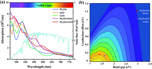
We also performed calculations of carrier mobility for the Pb2SSe/XSe (X = Sn/Ge) heterostructures, as listed in Table S6.† In comparison with the Pb2SSe monolayer, the electron mobilities of the Pb2SSe/XSe (X = Sn/Ge) heterostructures along both the x and y directions have been significantly improved. In particular, for the Pb2SSe/SnSe heterostructure, the electron mobility is up to 7.73 × 104 cm2 V−1 s−1, which is much larger than that of black phosphorus (1 × 104 cm2 V−1 s−1),68 implying the high carrier activity of the Pb2SSe/XSe (X = Sn/Ge) heterostructures. In addition, the good absorption capability of visible light is also an important factor for determining the efficiency of solar cells. In Fig. 6(a), we obtained the absorption coefficients for Pb2SSe, SnSe, GeSe monolayers and Pb2SSe/XSe (X = Sn/Ge) heterostructures with respect to the wavelength, which were calculated according to eqn (S5).† It can be found that the optical absorption intensity of the Pb2SSe monolayer along the x direction can reach up to 5.4 × 105 cm−1. For the Pb2SSe/XSe (X = Sn/Ge) heterostructures, the light absorption intensities along the x direction are much enhanced compared with the monolayers in the ultraviolet range and the visible light region (wavelength ranging from 550 to 630 nm). Moreover, the light absorption capability along the y direction (Fig. S9†) has a similar trend to the x direction but is slightly lower than the x direction.
 |
| | Fig. 6 (a) The optical absorption spectrum of the monolayer Pb2SSe, SnSe, GeSe Pb2SSe/SnSe, and Pb2SSe/GeSe heterostructures along the x direction. (b) Schematic diagram of exciton solar energy efficiency of the designed vdW heterostructures. | |
Owing to the small CBO (0.164 and 0.141 eV) and suitable donor band gap (1.37 and 1.59 eV) together with high carrier mobility and excellent light absorption capability of the Pb2SSe/XSe (X = Sn/Ge) heterostructures, it can be anticipated that they will be highly promise to design high-quality excitonic solar cells. The power conversion efficiencies (PCE) of Pb2SSe/XSe (X = Sn/Ge) heterostructures were calculated according to eqn (S6).† In Fig. 6(b), we present the PCE contour of the Pb2SSe/XSe (X = Sn/Ge) heterostructures. The calculated PCE values are as high as 20.02% and 19.28% for Pb2SSe/SnSe and Pb2SSe/GeSe heterostructures, respectively, which show an advantage over most other 2D vdW heterostructures (such as bilayer Janus Ga2SeTe (19%),69 SnSe/SnS (18%),29 MoSeTe/WSTe (18.32%),16 and bilayer phosphorene (18%)8).
3.5 Thermoelectric properties
The direct assessment for the thermoelectric performance of TE materials is its figure of merit (ZT), as determined by ZT = S2σT/κ, where S, σ, κ, and T represent the Seebeck coefficient, electrical conductivity, total thermal conductivity of electron thermal conductivity (κe) and lattice thermal conductivity (κL), and temperature, respectively. It can be inferred that the larger the numerator and the smaller the denominator, the higher the ZT value of the TE material. Thus, the higher the thermopower PF (PF = S2σ), the lower the intrinsic lattice thermal conductivity (κ), and the higher the thermoelectric conversion efficiency it holds. In this section, utilizing semi-classical Boltzmann theory for electron and phonon transport, we investigated the TE properties of the Pb2SSe monolayer.
It has been established that complex anisotropic and anharmonic structure and heavy element in 2D materials will cause large phonon scattering, resulting in low lattice thermal conductivity.70 For comparison, we predicted the lattice thermal conductivities of PbS, PbSe, and Pb2SSe monolayers using phonon transport calculations and the obtained κL as a function of the temperature is presented in Fig. 7(a). It can be found that κL decreases with the increase in the temperature following an inverse relation, and these monolayers exhibit ultralow κL close to 1 at room temperature. Such low value is lower than the well-known GeSe (5.81 W m−1 K−1), SnSe (3.64 W m−1 K−1), and α-Te (4.2 W m−1 K−1) monolayers,12,42 and is even comparable to the recognized single-layered Bi2O2Se (0.66 W m−1 K−1), InP3 (0.63 W m−1 K−1), and CdS (0.78 W m−1 K−1).38,62,71 In particular, the ranking of κL at 300 K can be arranged as Pb2SSe-x (0.78 W m−1 K−1) < PbSe (0.83 W m−1 K−1) < Pb2SSe-y (0.99 W m−1 K−1) < PbS (1.02 W m−1 K−1), confirming the advantages of the Janus structure in promoting phonon scattering and inhibiting heat transport in comparison with their pristine monolayers. On the basis of the definition of lattice thermal conductivity  , in which ν, τph, and c represent phonon group velocity, phonon lifetime, and specific heat, respectively, we then elucidated the phonon modes properties (ν and τph) to figure out the internal mechanism of the ultralow intrinsic κL of the Pb2SSe monolayer. Phonon mean free path (MFP), which is equal to the product of ν and τph, is an effective indicator of κL. Fig. 7(b) displays the cumulative lattice thermal conductivity with respect to the phonon MFP along the x and y directions. We can see that almost all phonons possess MFP under 130 nm and 180 nm along the x and y directions, respectively, and the phonons with MFP under 30 nm and 40 nm along the x and y directions contribute more than 2/3 of the total κL. Meanwhile, from the phonon modes contributions, as shown in Fig. S10,† it can be inferred that the contribution of 2/3 of the total κL is mainly from the acoustic branches (ZA, TA, and LA). Such low MFP indicates low phonon group velocity and phonon lifetime, as well as low lattice thermal conductivity. The phonon velocity (ν), a key factor to determine the phonon thermal transport, was calculated as plotted in Fig. 7(c). It can be observed that a majority of the phonons have speeds of less than 4 km s−1, which is lower than that of GeSe (4.5 km s−1) and phosphorene (7.7 km s−1).42,71 The phonon lifetime (τph), a critical parameter dominating phonon anharmonicity, and the three-phonon scattering phase space (P3), a quantization of the space available for the three-phonon process allowed by the conservation of the energy, were obtained in Fig. 7(d) and (e). The acoustic branches exhibit longer lifespan compared with the optical branches but the average phonon lifetime of about 6 ps is slightly lower than the well-known 2D triphosphides (<102 ps).72 The short phonon lifetime can be traced back to its relatively large P3 for the convenience of three-phonon scattering processes. Furthermore, the mode Grüneisen parameter (γ) is another significant parameter to describe the phonon anharmonic scattering and the larger the γ, the stronger the phonon anharmonicity. From Fig. 7(f), one can note that the acoustic phonons possess huge Grüneisen parameters (nearly −30), indicating the strong phonon anharmonic scattering and low κL in the Pb2SSe monolayer.
 |
| | Fig. 7 (a) The κL relative to the temperature and (b) the cumulative κL as a function of phonon MFP for PbS, PbSe, and Pb2SSe monolayers. (c) Group velocity of the phonons, (d) phonon relaxation lifetime, (e) P3 phase space, and (f) Grüneisen parameter (γ) for the Pb2SSe monolayer with respect to the frequency at 300 K. | |
Combining the temperature dependence of relaxation time τ (Fig. S11†), the electronic transport coefficients (S, σ, and PF) of the Pb2SSe monolayer were obtained according to eqn (S7)–(S11).†Fig. 8(a) shows the Seebeck coefficient of the p- and n-type Pb2SSe monolayer along the x and y directions with respect to the carrier concentration at 300 K. It can be noted that the absolute value of S shows a nearly linear descent versus the carrier concentration and exhibits a relatively small anisotropy along the x and y directions. In addition, as illustrated in Fig. 8(b), the electrical conductivity (σ) presents an exponential increase as the carrier concentration increases, showing the opposite trend to the Seebeck coefficient. Owing to the relatively different carrier relaxation times, σ exhibits remarkable anisotropy along the x and y directions and the maximum value of σ can reach 1.19 × 10⁵ S m−1, which is higher than most of the excellent TE materials previously reported.38,73 In addition, σ under n-type doping shows an advantage over the p-type one, which can be attributed to its higher electron mobility. According to the definition of PF, since S and σ show opposite trends with respect to the carrier concentrations, they will encounter a compromise between the decreasing function of S and increasing function of σ. As shown in Fig. 8(c), the obtained PF first shows an upward tendency, peaking at a certain concentration, and then decrease with the increase in the concentration. Owing to the high S and superhigh σ, the n-type PF along the x direction is markedly larger than the other 3 types and the maximum PF can reach 16.35 mW m−1 K−2 at 5.9 × 1012 cm−2, which is more than 5 times larger than that of 2D Bi2O2Se (3 mW m−1 K−2).38 Furthermore, we present the temperature dependence of Seebeck coefficient, electrical conductivity, and power factor at the optimal doping level as the temperature ranges from 300 to 700 K, as plotted in Fig. 8(d–f). It can be observed that the absolute value of S increases linearly with increasing temperature, the σ is strongly affected by the temperature and decreases inversely with the increase in temperature, while PF presents a linear decrease as the temperature increases. Overall, at the optimal concentration, the PF along the x direction is superior to that in the y direction due to the higher power factor and more favorable conductivity.
 |
| | Fig. 8 (a–c) The values of S, σ, and PF for p- and n-type doping along the x and y directions as a function of carrier concentrations at 300 K. (d–f) The temperature dependence of S, σ, and PF at the optimal doping concentration. | |
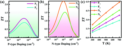
Based on the above calculated phonon and electronic transport coefficients, the figure of merit (ZT) of Pb2SSe monolayer can be estimated, and the results are illustrated in Fig. 9. At room temperature, as presented in Fig. 9(a) and (b), it can be found that ZT under n-type doping is relatively higher than that under p-type doping along the x and y directions, which can be ascribed to the higher PF and lower κL along the x direction. Specifically, the maximum ZT value is 2.19 (1.52) for n-type doping and 1.16 (0.91) for p-type doping along the x(y) direction at 300 K. Moreover, Fig. 9(c) shows the temperature dependence of ZT of the p- and n-type doping along the x and y directions. The maximum ZT values exhibit a linear increase when the temperature gradually increases, and they can reach 5.91 (4.58) for n-type doping and 3.75 (2.89) for p-type doping along the x(y) direction at 700 K. Such high ZT value of the Pb2SSe monolayer is much better than that of the well-known monolayer SnSe (2.32) and it can be expected that the Pb2SSe monolayer will be a high-performance TE material.42
 |
| | Fig. 9
ZT values for (a) p-type and (b) n-type doping with respect to the carrier concentration along the x and y directions. (c) Maximum ZT values of p- and n-type doping along the x and y directions for the Pb2SSe monolayer. | |
4. Conclusion
In this work, a systematic theoretical investigation about a neoteric anisotropic Janus monolayer Pb2SSe has been carried out utilizing first-principles calculations. The all-round verification about kinetic, thermal, and mechanical stability has been firstly performed by the calculation of phonon dispersion, AIMD simulation, and elastic constants. The electronic properties unveil that the Pb2SSe monolayer possesses an intrinsic indirect band gap of 1.59 eV, high carrier mobility (526–2105 cm2 V−1 s−1), and the characteristic of biaxial strain-adjusted to the direct band structure when (1%–3%) tensile strain is applied. The mechanical properties and piezoelectric coefficients of the Pb2SSe monolayer show that it has high mechanical flexibility, giant in-plane piezoelectricity of d11 = 75.1 pm V−1, and superhigh out-of-plane piezoelectric coefficients (d31 = 0.5 pm V−1 and d33 = 15.7 pm V−1). In the meantime, the out-of-plane piezoelectric coefficients are significantly enhanced (d31 = 19.2 pm V−1 and d33 = 194.7 pm V−1) through the construction of Pb2SSe bilayers, which can be attributed to the interlayer vdW interactions. Moreover, by means of building type-II vdW heterostructures with SnSe and GeSe monolayers, the Pb2SSe/SnSe and Pb2SSe/GeSe heterostructures exhibit favorable excitonic solar conversion efficiencies of 20.02% and 19.28%, respectively. Meanwhile, the calculated superhigh electron mobility (up to 7.73 × 104 cm2 V−1 s−1) and high visible-light adsorption capability (up to 6 × 105 cm−1) further promote its promising photovoltaic performance. Furthermore, the Pb2SSe monolayer also displays outstanding TE performance and its ZT value can reach 2.19 (1.52) for n-type doping and 1.16 (0.91) for p-type doping along the x(y) direction at 300 K. The high ZT value along the x direction at 300 K is mainly because of its ultralow κL = 0.78 W m−1 K−1, resulting from its low phonon velocities and short phonon lifetimes, and high PF = 10.18 (8.25) mW m−1 K−2 for n-type (p-type) doping at 300 K, tracing back to its high S and superhigh σ. This work demonstrates the Janus Pb2SSe monolayer displays great prospects for efficiently utilizing clean energy, which is also conducive for stimulating its further experimental fabrication.
Conflicts of interest
The authors declare no competing financial interest.
Acknowledgements
This research was financially supported in part by the National Natural Science Foundation of China (grant 62071073), in part by the Fundamental Research Funds for Central Universities (grant 2019CDJGFGD007), in part by the Innovation Project of GUET Graduate Education (grant 2021YCXS018), in part by the Key Science and Technology Program of Chongqing (grant CSTC2017SHMS-ZDYFX0028), in part by the Technology Innovation and Application Project of Chongqing (grant cstc2018jszx-cyzdX0111) and in part by the Guangxi Key Laboratory of Manufacturing Systems and Advanced Manufacturing Technology (grant 19-050-44-002K).
Notes and references
- D. L. Li, Y. N. Gong, Y. X. Chen, J. M. Lin, Q. Khan, Y. P. Zhang, Y. Li, H. Zhang and H. P. Xie, Nano-Micro Lett., 2020, 12, 1–40 Search PubMed.
- X.-L. Shi, J. Zou and Z.-G. Chen, Chem. Rev., 2020, 120, 7399–7515 CrossRef CAS PubMed.
- K. S. Novoselov, A. K. Geim, S. V. Morozov, D. Jiang, Y. Zhang, S. V. Dubonos, I. V. Grigorieva and A. A. Firsov, Science, 2004, 306, 666 CrossRef CAS PubMed.
- C. Kumunda, A. S. Adekunle, B. B. Mamba, N. W. Hlongwa and T. T. I. Nkambule, Front. Mater., 2021, 7, 616787 CrossRef.
- P. Geng, S. Zheng, H. Tang, R. Zhu, L. Zhang, S. Cao, H. Xue and H. Pang, Adv. Energy Mater., 2018, 8, 1703259 CrossRef.
- Y. Liu, X. Duan, H.-J. Shin, S. Park, Y. Huang and X. Duan, Nature, 2021, 591, 43–53 CrossRef CAS PubMed.
- Z. Ma, Z. Cui, C. Xiao, W. Dai, Y. Lv, Q. Li and R. Sa, Nanoscale, 2020, 12, 1541–1550 RSC.
- J. Dai and X. C. Zeng, J. Phys. Chem. Lett., 2014, 5, 1289–1293 CrossRef CAS PubMed.
- A. Patel, D. Singh, Y. Sonvane, P. B. Thakor and R. Ahuja, ACS Appl. Mater. Interfaces, 2020, 12, 46212–46219 CrossRef CAS PubMed.
- X. Du, J. Qiu, S. Deng, Z. Du, X. Cheng and H. Wang, ACS Sustainable Chem. Eng., 2020, 8, 5799–5806 CrossRef CAS.
- Y. Wu, K. Xu, C. C. Ma, Y. Chen, Z. X. Lu, H. Zhang, Z. L. Fang and R. J. Zhang, Nano Energy, 2019, 63, 103870 CrossRef CAS.
- J. Ma, F. Meng, J. He, Y. Jia and W. Li, ACS Appl. Mater. Interfaces, 2020, 12, 43901–43910 CrossRef CAS.
- R. Li, Y. Cheng and W. Huang, Small, 2018, 14, 1802091 CrossRef PubMed.
- R. Sant, M. Gay, A. Marty, S. Lisi, R. Harrabi, C. Vergnaud, M. T. Dau, X. Weng, J. Coraux, N. Gauthier, O. Renault, G. Renaud and M. Jamet, npj 2D Mater. Appl., 2020, 4, 41 CrossRef CAS.
- D. B. Trivedi, G. Turgut, Y. Qin, M. Y. Sayyad, D. Hajra, M. Howell, L. Liu, S. Yang, N. H. Patoary, H. Li, M. M. Petrić, M. Meyer, M. Kremser, M. Barbone, G. Soavi, A. V. Stier, K. Müller, S. Yang, I. S. Esqueda, H. Zhuang, J. J. Finley and S. Tongay, Adv. Mater., 2020, 32, 2006320 CrossRef CAS.
- A. Rawat, M. K. Mohanta, N. Jena, Dimple, R. Ahammed and A. De Sarkar, J. Phys. Chem. C, 2020, 124, 10385–10397 CrossRef CAS.
- R. Peng, Y. Ma, B. Huang and Y. Dai, J. Mater. Chem. A, 2019, 7, 603–610 RSC.
- M. Xiong, Z.-Y. Chen, C.-E. Hu, Y. Cheng and H.-Y. Geng, Mater. Today Commun., 2021, 26, 101995 CrossRef CAS.
- W. Wu, L. Wang, Y. Li, F. Zhang, L. Lin, S. Niu, D. Chenet, X. Zhang, Y. Hao, T. F. Heinz, J. Hone and Z. L. Wang, Nature, 2014, 514, 470–474 CrossRef CAS PubMed.
- Y. L. Zhou, W. Liu, X. Huang, A. H. Zhang, Y. Zhang and Z. L. Wang, Nano Res., 2016, 9, 800–807 CrossRef CAS.
- R. Ahammed, N. Jena, A. Rawat, M. K. Mohanta, Dimple and A. De Sarkar, J. Phys. Chem. C, 2020, 124, 21250–21260 CrossRef CAS.
- R. Fei, W. Li, J. Li and L. Yang, Appl. Phys. Lett., 2015, 107, 173104 CrossRef.
- H. Yin, J. Gao, G.-P. Zheng, Y. Wang and Y. Ma, J. Phys. Chem. C, 2017, 121, 25576–25584 CrossRef CAS.
- L. Dong, J. Lou and V. B. Shenoy, ACS Nano, 2017, 11, 8242–8248 CrossRef CAS PubMed.
- Y. Guo, S. Zhou, Y. Bai and J. Zhao, Appl. Phys. Lett., 2017, 110, 163102 CrossRef.
- Y. Chen, J. Liu, J. Yu, Y. Guo and Q. Sun, Phys. Chem. Chem. Phys., 2019, 21, 1207–1216 RSC.
- X. Li, W. Chen, S. Zhang, Z. Wu, P. Wang, Z. Xu, H. Chen, W. Yin, H. Zhong and S. Lin, Nano Energy, 2015, 16, 310–319 CrossRef CAS.
- W. Wang, M. T. Winkler, O. Gunawan, T. Gokmen, T. K. Todorov, Y. Zhu and D. B. Mitzi, Adv. Energy Mater., 2014, 4, 1301465 CrossRef.
- X. Lv, W. Wei, C. Mu, B. Huang and Y. Dai, J. Mater. Chem. A, 2018, 6, 5032–5039 RSC.
- N. Miao, B. Xu, N. C. Bristowe, J. Zhou and Z. Sun, J. Am. Chem. Soc., 2017, 139, 11125–11131 CrossRef CAS PubMed.
- K. Wu, H. H. Ma, Y. Z. Gao, W. Hu and J. L. Yang, J. Mater. Chem. A, 2019, 7, 7430–7436 RSC.
- H. Yang, Y. Ma, Y. Liang, B. Huang and Y. Dai, ACS Appl. Mater. Interfaces, 2019, 11, 37901–37907 CrossRef CAS PubMed.
- F. Li, W. Wei, H. Wang, B. Huang, Y. Dai and T. Jacob, J. Phys. Chem. Lett., 2019, 10, 559–565 CrossRef PubMed.
- K. Zhang, Y. Guo, Q. Ji, A.-Y. Lu, C. Su, H. Wang, A. A. Puretzky, D. B. Geohegan, X. Qian, S. Fang, E. Kaxiras, J. Kong and S. Huang, J. Am. Chem. Soc., 2020, 142, 17499–17507 CrossRef CAS PubMed.
- M. K. Mohanta and A. De Sarkar, Nanoscale, 2020, 12, 22645–22657 RSC.
- L. D. Hicks and M. S. Dresselhaus, Phys. Rev. B: Condens. Matter Mater. Phys., 1993, 47, 16631–16634 CrossRef CAS PubMed.
- S. Huang, Z. Y. Wang, R. Xiong, H. Y. Yu and J. Shi, Nano Energy, 2019, 62, 212–219 CrossRef CAS.
- J. B. Yu and Q. Sun, Appl. Phys. Lett., 2018, 112, 053901 CrossRef.
- S. D. Guo, Y. F. Li and X. S. Guo, Comput. Mater. Sci., 2019, 161, 16–23 CrossRef CAS.
- L. Xu, M. Yang, S. J. Wang and Y. P. Feng, Phys. Rev. B, 2017, 95, 235434 CrossRef.
- S. D. Guo and Y. H. Wang, J. Appl. Phys., 2017, 121, 7 Search PubMed.
- X. L. Zhu, C. H. Hou, P. Zhang, P. F. Liu, G. F. Xie and B. T. Wang, J. Phys. Chem. C, 2020, 124, 1812–1819 CrossRef CAS.
- G. Kresse and J. Furthmuller, Phys. Rev. B: Condens. Matter Mater. Phys., 1996, 54, 11169–11186 CrossRef CAS.
- J. J. Mortensen, L. B. Hansen and K. W. Jacobsen, Phys. Rev. B: Condens. Matter Mater. Phys., 2005, 71, 11 CrossRef.
- G. Kresse and D. Joubert, Phys. Rev. B: Condens. Matter Mater. Phys., 1999, 59, 1758–1775 CrossRef CAS.
- P. E. Blochl, Phys. Rev. B: Condens. Matter Mater. Phys., 1994, 50, 17953–17979 CrossRef PubMed.
- J. Heyd, G. E. Scuseria and M. Ernzerhof, J. Chem. Phys., 2003, 118, 8207–8215 CrossRef CAS.
- S. Grimme, J. Antony, S. Ehrlich and H. Krieg, J. Chem. Phys., 2010, 132, 154104 CrossRef PubMed.
- X. Gonze and C. Lee, Phys. Rev. B: Condens. Matter Mater. Phys., 1997, 55, 10355–10368 CrossRef CAS.
- L. Chaput, A. Togo, I. Tanaka and G. Hug, Phys. Rev. B: Condens. Matter Mater. Phys., 2011, 84, 6 CrossRef.
- W. Li, J. Carrete, N. A. Katcho and N. Mingo, Comput. Phys. Commun., 2014, 185, 1747–1758 CrossRef CAS.
- G. K. H. Madsen, J. Carrete and M. J. Verstraete, Comput. Phys. Commun., 2018, 231, 140–145 CrossRef CAS.
- H. Abouelkhair, P. N. Figueiredo, S. R. Calhoun, C. J. Fredricksen, I. O. Oladeji, E. M. Smith, J. W. Cleary and R. E. Peale, MRS Adv., 2018, 3, 291–297 CrossRef CAS.
- F. G. Hone, F. K. Ampong, R. K. Nkum and F. Boakye, J. Mater. Sci.: Mater. Electron., 2017, 28, 2893–2900 CrossRef CAS.
- Y. Mao, C. Xu, J. Yuan and H. Zhao, J. Mater. Chem. A, 2019, 7, 11265–11271 RSC.
- C. E. Ekuma, J. Phys. Chem. Lett., 2018, 9, 3680–3685 CrossRef CAS PubMed.
- W. Wan, Y. Yao, L. Sun, C.-C. Liu and F. Zhang, Adv. Mater., 2017, 29, 1604788 CrossRef.
- S. Maintz, V. L. Deringer, A. L. Tchougréeff and R. Dronskowski, J. Comput. Chem., 2016, 37, 1030–1035 CrossRef CAS PubMed.
- L.-M. Yang, V. Bačić, I. A. Popov, A. I. Boldyrev, T. Heine, T. Frauenheim and E. Ganz, J. Am. Chem. Soc., 2015, 137, 2757–2762 CrossRef CAS PubMed.
- T. V. Vu, C. V. Nguyen, H. V. Phuc, A. A. Lavrentyev, O. Y. Khyzhun, N. V. Hieu, M. M. Obeid, D. P. Rai, H. D. Tong and N. N. Hieu, Phys. Rev. B, 2021, 103, 085422 CrossRef CAS.
- Y. H. Robin Chang, T. L. Yoon, K. H. Yeoh and T. L. Lim, Int. J. Energy Res., 2021, 45, 2085–2099 CrossRef CAS.
- M. K. Mohanta and A. De Sarkar, ACS Appl. Mater. Interfaces, 2020, 12, 18123–18137 CrossRef CAS PubMed.
- R. Q. Zhang, Z. Z. Zhou, N. Qi, B. Zhao, Q. K. Zhang, Z. Y. Zhang and Z. Q. Chen, J. Mater. Chem. C, 2019, 7, 14986–14992 RSC.
- H. Lang, S. Zhang and Z. Liu, Phys. Rev. B, 2016, 94, 235306 CrossRef.
- N. T. Hung, A. R. T. Nugraha and R. Saito, J. Phys. D: Appl. Phys., 2018, 51, 075306 CrossRef.
- C. Lee, X. D. Wei, J. W. Kysar and J. Hone, Science, 2008, 321, 385–388 CrossRef CAS PubMed.
- Z. Liu, J. Z. Liu, Y. Cheng, Z. H. Li, L. Wang and Q. S. Zheng, Phys. Rev. B: Condens. Matter Mater. Phys., 2012, 85, 5 Search PubMed.
- S. P. Koenig, R. A. Doganov, H. Schmidt, A. H. Castro Neto and B. Özyilmaz, Appl. Phys. Lett., 2014, 104, 103106 CrossRef.
- J. Wang, H. Guo, J. Xue, D. Chen, G. Yang, B. Liu, H. Lu, R. Zhang and Y. Zheng, Sol. RRL, 2019, 3, 1900321 CrossRef CAS.
- M. Samanta, T. Ghosh, S. Chandra and K. Biswas, J. Mater. Chem. A, 2020, 8, 12226–12261 RSC.
- T. Ouyang, E. L. Jiang, C. Tang, J. Li, C. Y. He and J. X. Zhong, J. Mater. Chem. A, 2018, 6, 21532–21541 RSC.
- Z. H. Sun, K. P. Yuan, Z. Chang, S. P. Bi, X. L. Zhang and D. W. Tang, Nanoscale, 2020, 12, 3330–3342 RSC.
- Z. B. Gao and J. S. Wang, ACS Appl. Mater. Interfaces, 2020, 12, 14298–14307 CrossRef CAS PubMed.
Footnote |
| † Electronic supplementary information (ESI) available. See DOI: 10.1039/d1nr03440e |
|
| This journal is © The Royal Society of Chemistry 2021 |
Click here to see how this site uses Cookies. View our privacy policy here. 
 a,
Jian
Qiu
a,
Jian
Qiu


 , in which ν, τph, and c represent phonon group velocity, phonon lifetime, and specific heat, respectively, we then elucidated the phonon modes properties (ν and τph) to figure out the internal mechanism of the ultralow intrinsic κL of the Pb2SSe monolayer. Phonon mean free path (MFP), which is equal to the product of ν and τph, is an effective indicator of κL. Fig. 7(b) displays the cumulative lattice thermal conductivity with respect to the phonon MFP along the x and y directions. We can see that almost all phonons possess MFP under 130 nm and 180 nm along the x and y directions, respectively, and the phonons with MFP under 30 nm and 40 nm along the x and y directions contribute more than 2/3 of the total κL. Meanwhile, from the phonon modes contributions, as shown in Fig. S10,† it can be inferred that the contribution of 2/3 of the total κL is mainly from the acoustic branches (ZA, TA, and LA). Such low MFP indicates low phonon group velocity and phonon lifetime, as well as low lattice thermal conductivity. The phonon velocity (ν), a key factor to determine the phonon thermal transport, was calculated as plotted in Fig. 7(c). It can be observed that a majority of the phonons have speeds of less than 4 km s−1, which is lower than that of GeSe (4.5 km s−1) and phosphorene (7.7 km s−1).42,71 The phonon lifetime (τph), a critical parameter dominating phonon anharmonicity, and the three-phonon scattering phase space (P3), a quantization of the space available for the three-phonon process allowed by the conservation of the energy, were obtained in Fig. 7(d) and (e). The acoustic branches exhibit longer lifespan compared with the optical branches but the average phonon lifetime of about 6 ps is slightly lower than the well-known 2D triphosphides (<102 ps).72 The short phonon lifetime can be traced back to its relatively large P3 for the convenience of three-phonon scattering processes. Furthermore, the mode Grüneisen parameter (γ) is another significant parameter to describe the phonon anharmonic scattering and the larger the γ, the stronger the phonon anharmonicity. From Fig. 7(f), one can note that the acoustic phonons possess huge Grüneisen parameters (nearly −30), indicating the strong phonon anharmonic scattering and low κL in the Pb2SSe monolayer.

